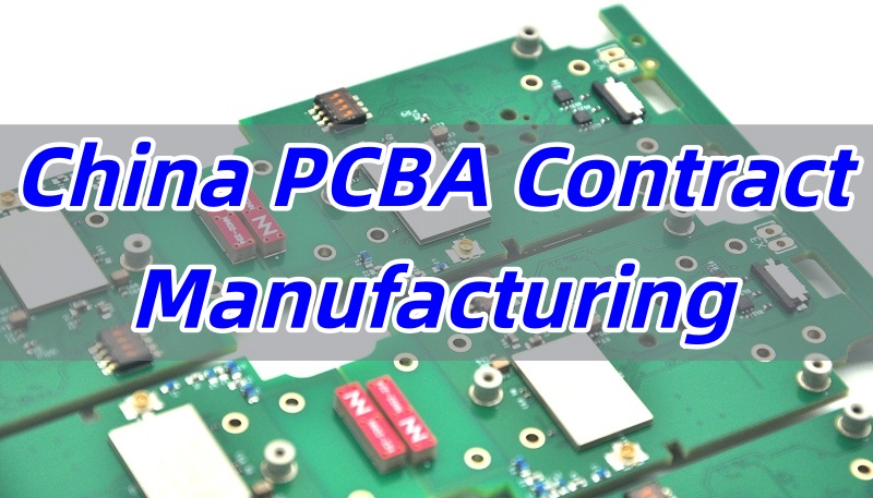
China PCBA manufacturer plays a pivotal role in the global electronics industry by bridging design concepts with reliable, mass-produced products. This article explains how China-based PCBA providers differ from non China PCBA manufacturers. It then shows practical selection criteria.
Do you face these challenges?
Uncertain prototype delivery timelines, slowing down R&D iterations.
High costs for small-batch production, making budget control difficult.
Unstable BOM component supply, risking shortages or delayed lead times.
Poor communication between design and manufacturing, causing repeated revisions and project delays.
Difficulty ensuring product quality and consistency, increasing risk before mass production.
To resolve the difficulties presented, pls kindly consider the following methods.
Dedicated prototype lines with transparent SLA (Service Level Agreement): Ensure fast prototype delivery and shorten R&D cycles.
Flexible small-batch production and cost optimization: Efficient production scheduling reduces small-batch manufacturing costs.
Strict BOM management and preferred supplier system: Identify critical component risks early and ensure timely supply.
Engineering-led DFM support and cross-functional collaboration: Optimize manufacturability during design to minimize rework.
Full-process quality control with MES traceability: Track all steps from SMT, through-hole assembly, testing to box-build integration to ensure consistency and reliability.
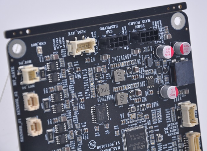
EBest Circuit (Best Technology) is a professional PCB manufacturer and SMT factory offering end-to-end PCB and PCBA solutions, from rapid PCB prototyping to turnkey assembly and box-build services. We specialize in rigid, flex, aluminum backed PCBs, alumina ceramic PCB, and rigid-flexible PCB boards, as well as PCB assembly, ensuring high-quality, reliable, and fully traceable production. Our core strengths include engineering-led DFM support, flexible production lines for prototypes and small batches, and strict process control to reduce rework and accelerate time-to-market. Contact us at sales@bestpcbs.com to request a quote or start a DFM review.
What are the features of a China PCBA manufacturer?
A mature China PCBA manufacturer bundles supply density, flexible capacity, engineering support, and traceability into one workflow.
Dense component ecosystem. China has many component distributors, PCB substrate vendors, and testing equipment suppliers within easy reach. This reduces sourcing time. It reduces freight costs. For prototype runs, that proximity converts to faster turnarounds.
Flexible production scale. Domestic factories can shift between small batches and volume runs. That helps teams running iterative designs. A single supplier can handle NPI and scale-up without repeated re-qualifications.
Integrated NPI and DFM support. Experienced manufacturers provide hands-on design-for-manufacturability (DFM) feedback early. They catch layout issues, BOM risks, and testability gaps before boards are fabricated.
Comprehensive testing and box build. Modern sites include AOI, X-ray, ICT, functional test stations and box build lines. The integration of assembly and final integration reduces handoffs and improves first-pass yield.
Traceability and process control. Good suppliers run MES to record lot history, operator steps and test results. That data matters when defects appear in the field. Traceability helps with root cause analysis.
Cost structure and speed. Lower direct labor cost and a mature supplier base allow competitive pricing. Faster component procurement shortens lead times for prototypes and standard builds.
In summary, a top-tier China PCBA manufacturer combines supply chain density, flexible production, engineering expertise, and strict process control to deliver fast, reliable, and cost-effective solutions from prototype to volume production.
Top 10 China PCBA prototyping manufacturers
PCBA prototyping plays a critical role in product development, bridging design concepts with functional verification and small-batch production. Choosing the right manufacturer is essential for fast iterations, cost control, and ensuring product reliability.
1. EBest Circuit (Best Technology)
Founded in 2006, EBest Circuit (Best Technology) provides a one-stop service from PCB design and materials procurement to full PCBA assembly. We serve high-end industries including 5G, automotive, and medical. Our facilities include SMT, X-ray, AOI, and functional test systems. We offer decent quality prototyping, fast delivery and accommodate small-batch orders.
2. PCBWay
A global leader in PCBA prototyping, PCBWay features highly automated production lines, multi-layer board capabilities, and supports fast prototyping.
3. ALLPCB
ALLPCB leverages its online platform for instant quoting, order placement, and rapid delivery. The company provides full-process quality inspection, including AOI, ICT, and functional testing. It enjoys high reputation in the global electronics maker community.
4. PCBGOGO
Specializing in small-to-medium batch PCBA, PCBGOGO offers full-chain services from component procurement to assembly. They can handle multi-layer, flexible, and high-frequency boards, enabling rapid prototype iterations.
5. Shenzhen Grande Electronic
Certified with ISO9001 and TS16949, Shenzhen Grande Electronic delivers fast prototypes, low-volume runs, and customized PCBA. They operate eight high-speed SMT lines, supporting high-density and high-reliability requirements.
6. Kunshan Quanhua Electronics
Known for its “one-stop” PCBA services, Quanhua Electronics covers component procurement, PCB fabrication, and functional testing. They excel at flexible switching between large and small batch production.
7. Seeed Fusion (Seeed Studio)
Integrating the open-source hardware ecosystem, Seeed Fusion provides rapid prototyping, flexible PCB production, and small-batch assembly. They own proprietary SMT equipment and comprehensive testing workflows, favored by makers and innovation-driven companies.
8. Jinghua Electronics
Jinghua Electronics supports multi-layer and rigid-flex PCB production, rapid prototyping, and full-process quality testing. They cater to small-batch customization and fast delivery requirements.
9. Shenzhen Jinghua
A notable candidate for ISO-certified, flexible, and fully tested PCBA prototypes with cross-border logistics experience, suitable for international clients seeking small-to-medium runs.
10. Other Worthy Candidates
Other noteworthy providers include Kunshan Quanhua and Shenzhen Grande. Key advantages include ISO certifications, flexible production, comprehensive testing, logistics expertise, and strong engineering support. These suppliers can be shortlisted for specific project needs.
To conclude, by comparing the core capabilities of these ten manufacturers, you can evaluate each supplier based on a structured checklist: delivery time, engineering support, testing capability, certifications, supply chain transparency, low-volume cost, system integration, IP security, logistics experience, and customer service. This method allows you to select the most suitable partner for prototyping projects, ensuring quality, cost efficiency, and timely delivery—ultimately improving the success rate of subsequent mass production.
What are the full China PCBA contract manufacturing process?
The contract manufacturing workflow is a sequence of controlled steps. Each step has clear deliverables and KPIs.
Design review and DFM — deliverable: DFM report and suggested BOM alternatives.
Validate footprints, tolerances, and test points.
Flag long-lead or obsolete parts.
BOM management and sourcing — deliverable: approved BOM and sourcing plan.
Cross-check each line item against multiple suppliers.
Use authorized distributors to reduce counterfeit risk.
PCB fabrication — deliverable: bare PCBs with fabrication report.
Specify stack-up, controlled impedance, and material selection.
Confirm thermal and mechanical constraints for assembly.
SMT and component placement — deliverable: assembled SMT boards.
Stencil design and process window setup are critical.
AOI during line stops defects early.
Thru-hole and mixed assembly — deliverable: assembled boards with through-hole components soldered.
Inspection and test — deliverable: test reports and C of C.
Run AOI, X-ray for BGAs, ICT for connectivity, and functional test per spec.
Record data to MES and attach to lot history.
Conformal coating / potting — deliverable: environmental protection per spec.
Box build and final validation — deliverable: fully integrated product and user-acceptance test (UAT) report.
Include wiring harnesses, mechanical frames, firmware programming and final burn-in.
Packing, labeling and logistics — deliverable: export-ready shipment with traceability labels and documentation.
KPIs to track (examples): first-pass yield, defect per million (DPM), on-time delivery, NPI time-to-volume, and test coverage rate. A serious supplier reports these metrics and acts on trends.
Core competencies: China PCB assembly manufacturers vs. non China PCBA manufacturers
The practical difference lies in supply chain proximity, scale economics, and flexibility during NPI. Below is a concise comparison across eight axes.
Supply chain density China: dense local vendors for capacitors, resistors, ICs, and substrates. Delivery windows tighten. Non China: longer import lead times in many regions.
Cost base China: lower direct labor and mature subcontracting. Non China: higher labor rates and often higher overhead per unit.
NPI agility China: many factories offer quick-turn prototypes and small runs. Non China: often optimized for stable volume production; prototyping may be slower.
Testing and equipment Both can host modern equipment. But China factories often scale equipment across many lines, lowering per-unit test costs.
Regulatory and certification Non China manufacturers may have local compliance advantages. China suppliers often hold the major international certifications needed for automotive, aerospace and medical.
IP and security Non China suppliers closer to end customers can ease IP concerns. China suppliers mitigate risk via NDAs, restricted access and contracted security workflows.
Logistics and lead time risk China: fast regional sourcing but dependent on sea/air freight. Non China: shorter inland transport for some customers, but may face longer component lead times.
Communication Non China: time-zone alignment can ease live collaboration. China: nominated PMs and structured reports solve most collaboration gaps.
In a nutshell, choose by priority. If fast prototyping, cost flexibility, and supplier depth matter, China suppliers often lead. If proximity, regulatory interpretation or single-source risk reduction matter more, a non China manufacturer may fit better. For many global teams, a hybrid model — design and prototyping in China, final assembly near end markets — balances risk and cost.
What are the core considerations when selecting a China PCB assembly manufacturer?
Use an evidence-based checklist to avoid wishful thinking. Below are the essential checks, in priority order.
Certifications and audit records: Ask for audit summaries, process maps and corrective action histories. Certificates alone are not proof — audit results are.
Traceability and MES: Probe whether the plant links board serials to component lot IDs and test outcomes. Traceability shortens root cause time.
Engineering and DFM depth: Request a recent DFM report and examples of design changes that prevented failures.
Test strategy and coverage: Compare AOI/X-ray/ICT/functional test scope to your risk profile. Ask for test reports from similar products.
Supply chain resilience: Check dual-source options, lead times for critical components, and local stocking policies.
Quality metrics: Obtain FPY, DPM and NCR trends for the last 12 months. Look for stable or improving trends.
Small-batch policy and pricing: Ensure clear pricing for prototypes and small volumes. Hidden setup fees are common; demand transparency.
Box-build competencies: Verify capability for harnesses, sub-assemblies, firmware programming and final UAT procedures.
Communication and PM structure: Ask who your point-of-contact is, how often you will receive updates, and the escalation path for issues.
Use supplier scorecards. Re-run scoring every six months. That maintains continuous improvement.
Why choose EBest Circuit (Best Technology) as your reliable China PCBA manufacturer?
EBest Circuit (Best Technology) combines engineering-first service, traceable processes, and flexible box-build lines to solve common customer pain points.
Customer pain points and EBest Circuit (Best Technology) responses:
Pain: Unclear lead times and late prototypes. Response: Dedicated prototype lines and a transparent prototyping SLA shorten turnaround and set clear expectations.
Pain: Hidden cost from component shortages or rework. Response: BOM risk alerts and preferred vendor lists help avoid last-minute premium buys. MES-based lot tracking reduces rework incidence.
Pain: Poor NPI support and repeated design fixes. Response: Hands-on DFM workshops with cross-functional engineers reduce revisions and speed approvals.
Competitive edges:
Multi-standard certifications that support automotive, medical and aerospace needs.
MES traceability across PCB fabrication, placement, testing and box build.
Integrated engineering teams for DFM, firmware support and in-line test development.
Flexible lines for prototypes, small batches and volume manufacturing under one roof.
EBest Circuit (Best Technology) is a China PCBA manufacturer specializing in rapid PCB prototyping, turnkey assembly and box build services. We handle rigid, flex and mixed-technology boards with strict process control and full traceability. Our engineering team works with customers to reduce rework and shorten time-to-market. Contact us at sales@bestpcbs.com.
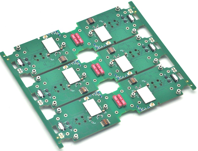
Case of PCBA manufacturing at EBest Circuit (Best Technology)
This case study highlights EBest Circuit (Best Technology)’s role as a key PCBA manufacturing partner for a leading innovator in the food service automation industry. We manufacture the critical main controller PCBA for our client’s product—an advanced intelligent cooking robot.
Our client aims to solve core industry challenges like food consistency, labor costs, and operational efficiency through automation. Their product is designed for demanding commercial kitchen environments characterized by high temperatures, humidity, and continuous operation. This placed stringent requirements on the core control PCBA:
High-Density Integration & Power Management: The main controller board needed to integrate complex motor control circuits (for precise stirring), high-power induction heating systems, and multiple sensor interfaces, ensuring perfect synchronization of all automated actions.
Superior Reliability & Thermal Management: The PCBA required robust components and a layout designed for effective heat dissipation to withstand long-term exposure to high ambient temperatures, ensuring device longevity and minimizing failure rates.
Absolute Manufacturing Consistency: Every single PCBA had to be built to identical industrial-grade quality standards to guarantee uniform performance across thousands of units deployed globally, which is fundamental to the client’s promise of consistent output.
As the designated SMT partner, we delivered engineering-driven manufacturing focused on robust process design for this complex controller board.
DFM & Process Optimization: Our engineering team optimized component placement and thermal management strategies during the DFM phase, ensuring reliability in high-temperature operating conditions.
Precision SMT & Mixed Technology: Advanced SMT equipment enabled accurate placement of fine-pitch components (0.4mm BGA, 0201), while maintaining reliable soldering for through-hole power connectors.
Full-Process Quality Assurance: Implementing SPI, AOI, in-circuit testing, and functional validation, supported by complete MES traceability for data-driven quality control.
In closing, EBest Circuit (Best Technology) ensured the AI cooking robot’s main controller PCBA met strict reliability, thermal, and performance standards through optimized DFM, precision SMT, and full-process quality control.
To wrap up, a good China PCBA manufacturer brings more than low unit costs. You gain speed, engineering leverage and integrated workflows that lower program risk.
If you need a partner that pairs fast prototypes with robust box-build services, EBest Circuit (Best Technology) aims to fill that role. We focus on tangible fixes for your pain points: predictable lead times, excellent quality, and hands-on engineering. Welcome to reach out to sales@bestpcbs.com to start a DFM review or request a prototype quote.
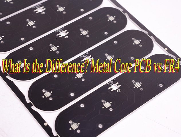
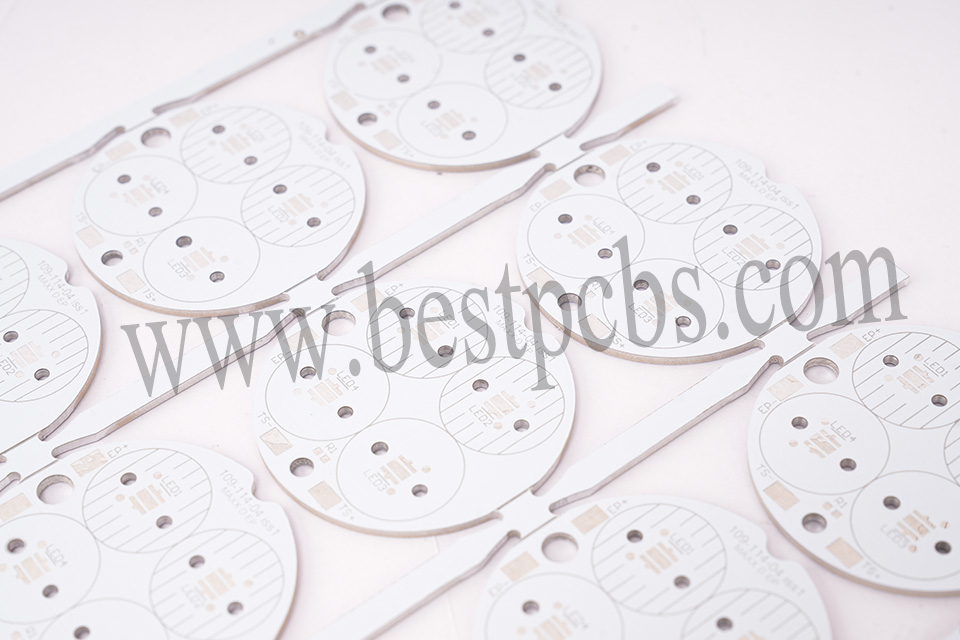
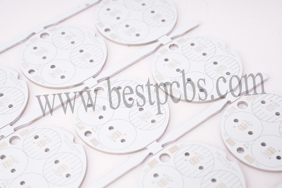
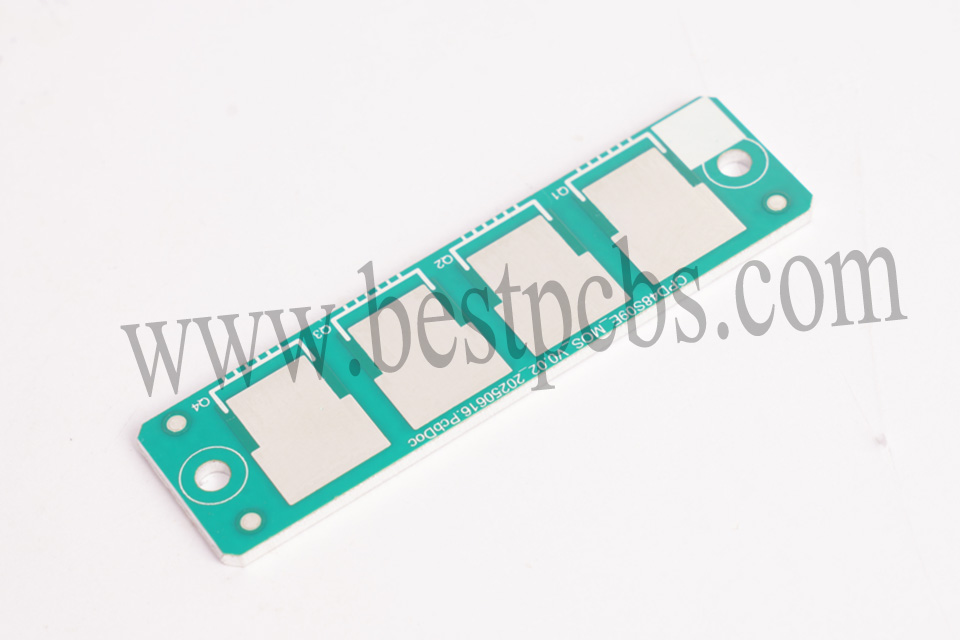
Which is difference between metal core PCBand FR4? This article compares the structural characteristics, thermal performance, and applicable scenarios of metal core and FR4 PCBs, providing accurate selection guidance.
A Metal Core PCB(MCPCB) is a printed circuit board with a metal base layer, typically aluminum or copper, designed for efficient heat dissipation in high-power applications. Its three-layer structure consists of copper circuitry, dielectric insulation, and metal core, enabling superior thermal management.
This makes it ideal for LED lighting, automotive electronics, and industrial power systems. The metal core acts as a heat sink, transferring heat away from components to prevent overheating while maintaining electrical insulation through the dielectric layer. This design ensures reliable performance in high-temperature environments.
What Is a FR4 PCB?
FR4 PCB is a printed circuit board made from FR-4 material, a flame-retardant glass fiber reinforced epoxy resin composite widely used in electronics due to its excellent mechanical strength, electrical insulation, and thermal stability.
It serves as a reliable substrate for mounting components while ensuring dimensional stability under varying environmental conditions. The material’s UL94 V-0 flammability rating and cost-effectiveness make it the standard choice for most consumer electronics, industrial equipment, and communication devices.
What Is the Difference? Metal Core PCB vs FR4
Material Composition & Structure
FR4 PCB: Manufactured from woven glass fiber impregnated with epoxy resin, this composite material offers insulation and mechanical strength. Its mature fabrication process supports multi-layer stacking for complex circuit designs, with copper traces plated on surfaces, ideal for standardized electronic module production.
Metal Core PCB: Built with aluminum or copper substrates in a “sandwich” architecture (circuit layer-insulation layer-metal base), the metal layer provides thermal support. Aluminum substrates are lightweight and cost-effective, while copper substrates deliver superior thermal conductivity (>380W/m·K). Insulation layers often use thermal silicone or ceramic-filled materials to balance electrical isolation and heat conduction.
Thermal Performance
FR4 PCB: Thermal conductivity ~0.3W/m·K, weak heat dissipation suitable for low-to-mid power applications. In LED modules or low-power supplies, external heatsinks are required to prevent thermal buildup that raises chip junction temperatures and shortens lifespan.
Metal Core PCB: Thermal conductivity ranges from 1-380W/m·K (aluminum: 1-3W/m·K, copper: >380W/m·K), achieving 6-9 times higher efficiency than FR4. For example, in automotive LED headlights, copper substrates rapidly dissipate heat from IGBTs, preventing light decay or burnout.
CTE Matching
FR4 PCB: Coefficient of Thermal Expansion (CTE) 12-24ppm/°C, significantly differing from copper’s 17ppm/°C, leading to delamination risks under thermal stress. Repeated thermal cycling may cause micro-cracks at FR4-copper interfaces, reducing electrical reliability.
Metal Core PCB: CTE closely matches copper (e.g., aluminum: 24ppm/°C), minimizing thermal cycling failure risks. The low CTE differential ensures stable electrical connections in high-reliability applications like aerospace or industrial control systems.
Mechanical Strength & Environmental Adaptability
FR4 PCB: Flexural strength ~480MPa, suitable for consumer electronics but prone to deformation under high temperature/pressure. While stable in everyday devices, it risks board fracture in vibration-heavy industrial environments.
Metal Core PCB: Metal substrates enhance rigidity, vibration/impact resistance, and suitability for extreme conditions like automotive electronics or industrial equipment. For instance, in new energy vehicle motor controllers, aluminum substrates withstand high-frequency vibrations and thermal shocks, ensuring circuit stability.
Electrical Performance
CDielectric constant 4.0-4.8, loss tangent 0.01-0.02, optimal for mid-to-low frequency signal transmission. Enables low-loss signal routing in communication devices, supporting high-frequency/high-speed designs.
Metal Core PCB: High-frequency performance depends on insulation layer design. While typically prioritized for thermal management, electrical performance slightly lags FR4. Optimized insulation materials (e.g., low-dielectric polymers) can balance high-frequency signal integrity with thermal efficiency.
Cost & Processing
FR4 PCB: Low cost, easy processing, and compatibility with complex multi-layer designs. Mass-produced by standard PCB factories at 1/3 to 1/5 the cost of metal core PCBs, ideal for large-scale consumer electronics.
Metal Core PCB: Higher costs due to specialized processing (e.g., metal substrate etching, precision drilling) and single/simple multi-layer structures. Despite elevated per-unit costs, long-term thermal management benefits reduce system maintenance expenses.
Application Scenarios
FR4 PCB: Dominates general-purpose fields like consumer electronics, communication devices, and home appliances (e.g., smartphone motherboards, router PCBs), leveraging low cost and mature processes for rapid iteration.
Metal Core PCB: Targets high-power, thermally demanding scenarios such as LED lighting, power modules, automotive electronics, and industrial equipment (e.g., streetlight drivers, EV battery management systems), optimizing thermal management to enhance device reliability.
Why Are Metal Core PCBs Better at Dissipating Heat than FR4 PCBs?
Reasons why MCPCB better at dissipating heat than FR4 PCB:
Direct Thermal Path via Metal Substrate: Aluminum/copper substrates in Metal Core PCBs create a vertical thermal channel from the chip through the insulating layer to the metal base. This bypasses FR4’s multi-layer dielectric thermal resistance stack-up, reducing thermal resistance by 60-90%. For example, in IGBT modules, copper-based PCBs can lower junction temperatures by 20-30°C, directly extending device lifespan.
Optimized Insulation Layer Materials: Metal Core PCBs use thermally conductive silicones, ceramic fillers (e.g., AlN), or nano-composites as insulating layers. These materials balance electrical isolation with high thermal conductivity (5-20W/m·K for AlN-filled layers vs. FR4’s 0.3W/m·K), creating a “thermal short-circuit” effect for rapid heat transfer.
Active Thermal Structure Design: Metal substrates can be machined with fins, thermal via arrays, or embedded heat pipes to actively expand surface area. In LED streetlights, aluminum substrates with radial fins increase heat dissipation area by 300%, enabling passive air cooling without additional fans.
Thermal-Mechanical Stability: Metal’s high rigidity minimizes thermal deformation impacts on circuits. In automotive power systems, aluminum substrates exhibit <0.1% warpage across -40°C to 125°C cycles, compared to FR4’s >0.5% deformation that risks solder joint fatigue.
System-Level Thermal Integration: Metal Core PCBs integrate directly with enclosures/heatsinks to form a unified thermal management chain. In 5G base station power modules, copper substrates bond with aluminum chassis for large-area passive cooling, reducing reliance on active cooling components and lowering system complexity/cost.
Why is Metal Core PCB More Suitable for High-Power Application Than FR4 PCB?
Superior Thermal Conductivity Materials
Metal core PCBs utilize copper (385 W/mK), aluminum (200 W/mK), or steel alloys with thermal conductivity 50-1000 times higher than FR4 (0.4 W/mK). This allows rapid heat dissipation from components, preventing thermal buildup-induced performance degradation or failure. For example, in 1000A automotive IGBT modules, copper substrates limit temperature rise to ≤30℃, while FR4 may trigger thermal protection due to localized overheating.
3D Heat Conduction Architecture
Thermal via arrays (0.1mm micro-vias at 100 holes/cm² density), embedded copper blocks (0.5-2mm thick), and metal backplate heat sinks form a tiered heat conduction path: component → thermal vias → substrate → external heatsink. This vertical heat transfer achieves 3-5 times higher efficiency than FR4’s planar heat spreading, ideal for high-power-density scenarios like LED streetlights and 5G base station PA modules.
Enhanced Heat Diffusion & Thermal Uniformity
High thermal diffusivity of metals (e.g., aluminum at 97 mm²/s) enables heat to spread evenly across the substrate within 0.1 seconds, avoiding localized hotspots that plague FR4 (thermal diffusivity: 0.3 mm²/s). During 150℃ thermal shock tests, metal core PCBs exhibit stable temperature profiles, whereas FR4 shows stepwise heating that risks component thermal stress cracking.
Low-Resistance Heat Dissipation Path
Direct contact between component pads and the metal substrate via high-conductivity solder (e.g., SnAgCu) achieves thermal resistance as low as 0.1℃/W—significantly lower than FR4’s insulation layer resistance (>10℃/W). This direct path minimizes interlayer thermal resistance accumulation, ensuring stable high-power operation.
Metal substrates withstand temperatures >300℃ (e.g., copper), while FR4 softens above 130℃, risking delamination or solder joint failure. Metal core PCBs pass 1000-hour 85℃/85%RH CAF (Conductive Anodic Filament) tests for corrosion resistance, outperforming FR4’s 500-hour limit and reducing long-term failure rates.
Extreme Environment Adaptability
In aerospace and deep-sea applications, metal core PCBs endure -55℃ to 125℃ temperature swings, high pressure, and salt spray without degradation. FR4, prone to moisture absorption and insulation breakdown, fails in such conditions—e.g., satellite power modules rely on steel alloy substrates for vacuum stability.
How Does Cost Difference between FR4 and Metal Core PCB?
The unit price of a standard double-sided FR4 PCB (1.6mm thickness) is approximately $2-$5 per piece. Leveraging a mature supply chain and the low-cost advantages of glass fiber substrates, it is suitable for large-scale mass production, with the unit price for an order of 10,000 pieces being reduced to $0.5 per piece. Metal core PCBs (MCPCBs) of the same size cost $15-$50 per piece, 7-10 times the cost of FR4.
This is mainly due to the high price of aluminum/copper core substrates (approximately $10-$30/㎡, 3-5 times the cost of FR4 substrates), the need for specialized surface treatment processes such as drilling and anodizing (which increase manufacturing costs by 30%-50%), and the difficulty in allocating processing losses in small-batch production, limiting the room for cost reduction.
How to Choose between Metal Core PCB and FR4 PCB?
Clarify Power Requirements & Thermal Constraints
High-power scenarios (≥50W/cm² heat density): Choose metal core PCB (aluminum/copper-based) for 6-9x higher thermal conductivity (1-380W/m·K vs. FR4’s 0.3W/m·K), preventing overheating in LED lighting, power modules, or automotive IGBTs.
Low-power scenarios (<20W/cm²): Optimize for FR4 due to lower cost and mature fabrication, ideal for consumer electronics and home appliances.
Evaluate Environmental Resilience
Extreme conditions (high temp/vibration/humidity): Metal core PCB’s rigid metal base (2-3x stronger than FR4) withstands shocks in automotive power systems or industrial drives.
Standard environments (indoor/low-vibration): FR4 suffices for basic mechanical strength in routers or phone motherboards.
Balance Cost & Long-Term Benefits
Budget-sensitive/mass production: FR4 wins with low material costs, complex multi-layer support, and quick scaling.
High reliability/longevity focus: Metal core PCB reduces secondary cooling costs (e.g., heat sinks/fans) and extends device life, justifying its higher unit cost in 5G power supplies.
Match Electrical & Signal Requirements
High-frequency applications (≥1GHz): FR4’s superior dielectric constant (4.0-4.8) and loss tangent (0.01-0.02) suit fine-line RF designs.
Thermal-priority scenarios (e.g., LED drivers): Metal core PCB balances heat dissipation with optimized insulators like thermal silicone.
Consider Thermal Expansion Compatibility
Frequent thermal cycling (outdoor/industrial control): Metal core’s CTE (e.g., aluminum: 24ppm/°C) aligns with copper traces (17ppm/°C), minimizing interface stress and delamination risk.
Stable thermal environments (indoor): FR4 works with stress-relief designs (e.g., thermal buffer layers) at lower cost.
Factor in Design Complexity & Manufacturability
Complex multi-layer/high-density interconnects: FR4’s mature processes support intricate stacking and fine-pitch routing.
Simple/single-layer thermal-centric designs: Metal core PCB’s streamlined structure reduces manufacturing complexity, ideal for cost-sensitive thermal applications.
Assess Sustainability & Recycling Potential
Eco-conscious projects: FR4’s glass-fiber/epoxy composition is recyclable via specialized processes, while metal core PCBs (aluminum/copper) offer higher material recovery rates, aligning with circular economy goals.
Why Choose EBest Circuit (Best Technology) as Your Metal Core PCB Manufacturer?
Mature Process Library & Parameterized Design Support: Leverage proven process libraries and parameterized design templates for single-layer to multi-layer metal-core substrates (aluminum/copper/iron-based), reducing trial-and-error costs by 30% and accelerating time-to-market for rapid iteration projects.
Dual Certification Compliance Guarantee: Meet stringent medical (ISO 13485) and automotive (IATF 16949) industry standards with dual certifications, shortening product launch cycles by 2-4 weeks and minimizing compliance risks for swift project validation.
24-Hour Rapid Prototyping Delivery: Enable same-day design validation closure and next-day physical prototype delivery for urgent needs, supporting fast design feasibility verification and market entry acceleration.
Full-Process 12-Step SPC Quality Control: Implement batch-specific CPK≥1.33 testing across thickness, thermal conductivity, and insulation resistance, ensuring ≥99.5% yield to minimize rework losses and provide reliable mass production assurance.
Transparent Tiered Pricing System: Eliminate hidden costs like mold/engineering fees, optimize metal material costs by 30% for bulk orders, and offer clear budgeting support for precise project cost management.
One-Stop Full-Process Service Chain: Cover end-to-end workflows from design support, prototyping, mass production, surface finishing (ENIG/OSP), to assembly testing, cutting multi-vendor coordination costs by 50% and freeing focus for core design optimization.
Free DFM Design Optimization: Proactively identify process risks (e.g., thermal stress, etching defects) to optimize layout and material selection, lowering production costs by 20% and enhancing manufacturability for seamless design-to-manufacturing transition.
Customized Thermal Management Solutions: Utilize high thermal conductivity materials (aluminum ≥2.0W/m·K, copper ≥380W/m·K) to design thermal vias, integrate heat sinks, and perform thermal simulations, ensuring ≤20℃ temperature rise in high-power scenarios for enhanced product reliability.
Welcome to contact us if you have any request for metal core PCBs: sales@bestpcbs.com.
China PCBA contract manufacturing has reshaped the electronics supply chain. This blog provides a comprehensive guide to China PCBA contract manufacturing, covering industry features, top companies, advantages of choosing Chinese PCBA contract manufacturers, selection tips, and real-world case studies from EBest Circuit (Best Technology).
Are You Struggling With These Common Challenges?
Unpredictable lead times: Small-batch prototypes or urgent orders often face delays.
Inconsistent quality: Poor soldering, component errors, or test failures can occur.
Slow communication: Design changes and technical issues may not be addressed promptly.
Unstable component supply: Key parts may be delayed or out of stock.
Limited technical support: Lack of guidance increases risks during design or production.
How Does BEST Technology Solve These Challenges?
Optimized production planning: Smart scheduling and multi-line SMT ensure fast delivery from prototypes to mass production.
PCBA contract manufacturing in China means outsourcing printed circuit board assembly to specialized companies. These partners manage each step carefully:
Component sourcing – locating original and certified parts.
Supply chain strength – easy access to parts, boards, and logistics.
Fast delivery – competitive lead times compared to other regions.
These strengths give customers a reliable way to move from design to mass production quickly.
How to Select Reliable PCB Contract Manufacturers?
Not every supplier offers the same level of service. To select a reliable partner, companies should:
Verify certifications to match industry needs.
Review inspection systems like AOI, ICT, and flying probe testing.
Check sourcing channels to avoid counterfeit risks.
Request project cases that prove capability.
Evaluate communication, response speed, and engineering support.
These points help companies avoid common problems such as delays or quality failures.
Case of PCBA Contract Manufacturing at EBest Circuit (Best Technology)
EBest Circuit (Best Technology) recently established a strategic partnership with a leading Swiss IoT monitoring solutions provider to manufacture high-reliability PCBA boards for their smart building and energy management systems. Our PCBA assemblies are widely used in the client’s energy collaborative consumption projects (ZEV), Flat Roof Monitoring System (Dach-Monitoring), and Filter Monitoring System (Filter-Monitoring), which have been successfully deployed across residential, commercial, and industrial buildings throughout Europe.
Application Scenario 1: Distributed Energy Management System
The PCBA boards designed and assembled by EBest Circuit (Best Technology) are integral to the client’s energy collaborative consumption projects (ZEV), which enables intelligent management of solar energy sharing and metering in multi-tenant residential buildings. Our boards feature multi-channel data acquisition capabilities, support real-time processing of smart meter data, and drive energy visualization and automated billing interfaces through wired or wireless communication.
📌 Key Functions of our PCBA Boards:
Multi-channel meter data acquisition and transmission
Energy distribution and consumption logic control
User-end data visualization support
Remote communication and alarm functionality
Application Scenario 2: Flat Roof Monitoring System
The same client utilizes our PCBA boards in their Flat Roof Monitoring System (Dach-Monitoring) for detecting water leakage and monitoring micro-climate conditions within flat roof structures. Our boards interface precisely with temperature and humidity sensors, transmit data reliably via LoRa networks, and trigger instant alerts through multi-channel notification systems when leaks are detected—effectively preventing structural damage and significantly reducing maintenance costs.
📌 Technical Highlights:
Low-power battery design supporting continuous operation for 8+ years
Multi-protocol communication compatibility for complex building environments
High-sensitivity water detection with rapid response time
Application Scenario 3: Predictive Filter Maintenance System
We also supplied PCBA boards for the client’s Filter Monitoring System (Filter-Monitoring), which optimizes HVAC operations through predictive maintenance. The boards incorporate high-precision sensors to collect real-time data on filter pressure, temperature, and humidity, utilize intelligent algorithms for analysis, and automatically notify facility managers when replacements are needed—achieving efficient resource utilization and significant carbon emission reduction.
📌 System Benefits:
Over 50% reduction in manual inspections and travel costs
Significant energy savings and CO₂ emission reduction
Value Delivered by EBest Circuit (Best Technology):
High-Reliability Design: All PCBA boards comply with ISO 13485medical device and IATF 16949 automotive electronics standards, suitable for demanding environments
Flexible Manufacturing Capabilities: Support for rigid, rigid-flex, and small-batch quick-turn PCB production to accommodate rapid product iterations
End-to-End Quality Control: Implementation of AOI, X-ray inspection, ICT testing, and multiple quality assurance processes ensuring long-term operational stability
Supply Chain Advantages: Leveraging local component supply networks and logistics capabilities to support agile delivery for European markets
Through this collaboration, EBest Circuit (Best Technology) has not only enhanced the functionality and reliability of the client’s IoT systems but also demonstrated our expertise in high-end industrial and building technology PCBA manufacturing, providing comprehensive solutions from design to mass production.
Certifications for automotive, medical, and aerospace projects.
Engineering guidance at each stage.
Strict quality control with modern inspection systems.
Full turnkey EMS solution from PCB prototypes, fabrication, SMT assembly, and box build.
We reduce pain points such as unclear communication or inconsistent quality. Our goal is to build long-term trust with customers.
To sum up, China PCBA contract manufacturing has transformed global supply chains by providing cost-efficient, high-quality, and fast services. While there are many Chinese PCB manufacturers, not all offer the same level of reliability. EBest Circuit (Best Technology) stands out by addressing customer pain points such as delays, inconsistent quality, and lack of engineering guidance. We’re here to partner with you on your PCB and PCBA projects. Contact our sales team at sales@bestpcbs.com.
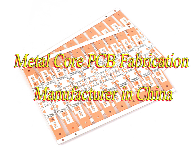
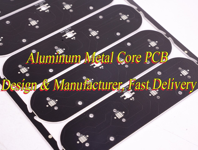
Looking for reliable metal core PCB fabricationmanufacturer? Let’s explore its definition, types, production process, recommended MCPCB manufacturer.
Are you worried about these problems?
Is long lead time for metal-core PCB delaying your project progress?
Struggling with high-power heat dissipation, forcing repeated thermal layout adjustments?
Balancing high material costs against performance needs in your budget?
As a MCPCB manufacturer, EBest Circuit (Best Technology) can provide service and solutions:
24-Hour Rapid Prototyping: Receive physical samples by next day, accelerating prototype validation without project delays.
Customized Thermal Management: Leverage aluminum-based (≥2.0W/m·K) and copper-based (≥380W/m·K) high thermal conductivity, combined with thermal simulation, to maintain ≤20℃ temperature rise in high-power applications.
Transparent Cost Control: No hidden fees, material costs reduced by 30%, with clear tiered pricing and bulk order discounts for precise budget planning.
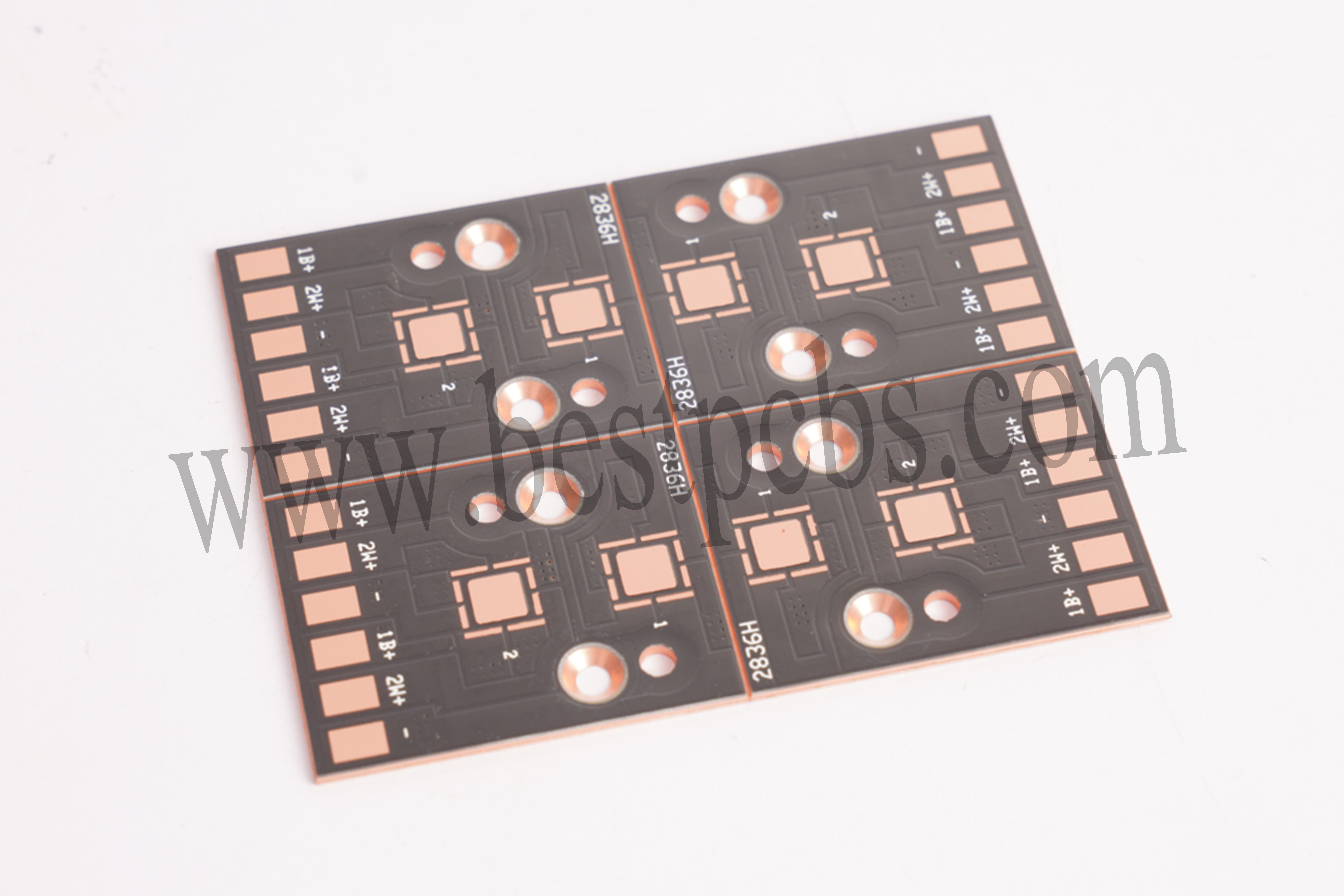
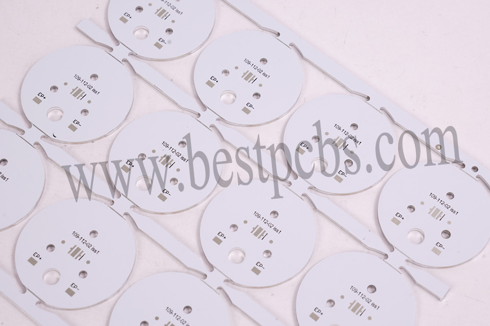
Metal Core PCB Fabrication refers to the process of manufacturing printed circuit boards using metal materials such as aluminum, copper, or steel alloys as the core heat dissipation layer through processes such as lamination, drilling, and surface treatment. Its core feature is the high thermal conductivity of the metal substrate to achieve efficient thermal management. It is widely used in scenarios that require rapid heat dissipation, such as LED lighting, power modules, automotive electronics, and high-power industrial equipment.
Types of Metal Core PCB Fabrication
Aluminum Core PCB: Using 5052/6061 aluminum alloy as the core material, it combines lightweight properties with high thermal conductivity (1-2W/mK or higher) and excellent cost-effectiveness. Widely applied in LED lighting, automotive electronics, and power modules, it supports single-layer to multi-layer structural designs to meet high-density integration and efficient heat dissipation requirements.
Copper Core PCB: Employing pure copper or copper alloy substrates, it offers superior thermal conductivity (exceeding 4W/mK) and significantly better heat dissipation efficiency compared to aluminum-based materials, though at a higher cost. Ideal for high-frequency circuits, high-power laser devices, and medical imaging equipment where extreme heat dissipation is critical, often enhanced with surface plating (e.g., immersion gold, silver plating) for improved solderability.
Iron-Core Metal PCB: Based on ordinary steel or stainless steel, it features high mechanical strength and better thermal conductivity than traditional FR-4 materials (though lower than aluminum/copper). Commonly used in precision scenarios requiring controlled thermal expansion coefficients, such as LED packaging, industrial power modules, and specific optical devices, balancing heat dissipation with structural stability.
Hybrid-Pressure Metal Core PCB: Combining metal substrates (e.g., aluminum/copper) with FR-4 or other insulating materials to form a composite structure. It balances signal integrity and heat dissipation needs, suitable for complex electronic systems requiring both high-frequency signal transmission and efficient heat management, such as 5G base station RF modules and industrial controllers.
Material Selection: Utilize C1100 pure copper substrate with thermal conductivity ≥380W/(m·K), thickness tolerance ±0.02mm, and surface roughness Ra≤0.8μm.
Precision Cutting: Cut to design dimensions (e.g., 100mm×100mm to 500mm×600mm) using CNC equipment, with edge chamfering to prevent burrs and dimensional accuracy ±0.05mm.
Surface Enhancement: Ultrasonic cleaning removes oil contaminants; sandblasting or chemical etching (sulfuric acid-hydrogen peroxide system) increases bonding strength, with roughness controlled at 1.5-3.0μm.
2. Circuit Production Full Workflow
Dry Film Application: Apply LDI-specific dry film (8-12μm thickness), use laser direct imaging (LDI) for high-precision transfer (line width/spacing ≥50μm), and set exposure energy at 100-150mJ/cm².
Etching Process: Alkaline etching solution (copper chloride system) operates at 45-50℃ with an etching rate of 1.0-1.5μm/min; spray systems ensure uniform etching, and side etching is limited to ≤0.05mm.
PP Lamination: High-Tg (≥170℃) semi-cured sheets (e.g., FR-4 epoxy) are heat-pressed (180-200℃, 3.0-4.0MPa) to eliminate bubbles and delamination.
Precision Drilling: CNC or laser drilling achieves hole diameter accuracy ±0.05mm, wall roughness Ra≤3.2μm, and cleanliness meeting IPC-6012 standards.
4. Lamination Process Optimization
High-Temperature High-Pressure Lamination: At 200-220℃ and 4.0-5.0MPa for 60-90 minutes, copper substrate and cover film fuse into a void-free integrated structure.
Stripping Treatment: NaOH solution (5-10%) at 50-60℃ removes residual dry film within 3-5 minutes without damaging copper circuits; pure water rinse and drying follow.
5. Surface Treatment and Protection
Solder Mask: Liquid photosensitive ink (20-30μm) is UV-cured to form a durable protective layer (temperature resistance ≥300℃, insulation ≥10¹²Ω) with precise patterning via development.
Character Printing: Screen-printed white/black ink cures at 150℃ for 60 minutes, ensuring smudge-free legibility and alcohol resistance ≥50 cycles.
Surface Finishes:
OSP: 0.2-0.5μm organic coating, lead-free and eco-friendly, ideal for short-term storage.
Immersion Gold: Au 0.05-0.1μm/Ni 3-5μm, excellent corrosion resistance for high-frequency applications.
Cutting Precision: CNC routing or laser cutting maintains ±0.1mm accuracy; V-CUT depth is controlled at 1/3-2/3 of board thickness, with burr-free edges.
Process Control: SPC monitoring with CPK≥1.33; real-time parameter tracking and automatic alarms at each inspection point.
Eco-Compliance: Waste etching solution is neutralized/precipitated for licensed disposal; waste gas undergoes activated carbon adsorption + catalytic combustion to meet ISO 14001 standards.
Traceable Packaging: Vacuum-sealed packaging with anti-moisture/oxidation protection; each batch includes QC reports, MSDS, RoHS certificates, and QR code traceability for full production data.
Substrate Metal Type Customization: Selectable aluminum-based, copper-based, iron-based, or composite metal alloy substrates, with thickness customization available from 0.5mm to 5mm, balancing thermal conductivity and cost efficiency.
Layer Count & Structural Configuration: Supports single-layer to 8-layer+ metal-core PCB structures, with flexible signal/power/ground layer distribution to accommodate high-density integration, high-frequency signal transmission, or high-power circuit requirements.
Thermal Management Specialized Design: Integrates thermal via arrays, thermal interface material (TIM) coatings, or finned heat sink topologies, leveraging high thermal conductivity of metal substrates for precise chip-to-system thermal path optimization.
Surface Finish Options: Offers surface treatments including ENIG (Electroless Nickel Immersion Gold), OSP (Organic Solderability Preservative), HASL (Hot Air Solder Leveling), and chemical nickel-gold, ensuring soldering reliability, oxidation resistance, and long-term stability.
Precision Line & Via Parameters: Supports 20μm minimum line width/spacing precision etching, with mechanical/laser drilling and blind/buried via capabilities for 0.1mm-1.0mm via diameters, meeting high-density interconnect demands.
Custom Shape & Contour Machining: Enables non-standard dimensions (e.g., circular, annular, polygonal) and complex contour cutting, including V-cut scoring, milling slots, and chamfering for device structural fit and assembly requirements.
Solder Mask & Identification Customization: Multi-color solder mask options (green, black, white, etc.), with customer-specified logo, model identification, and QR code etching for traceability and brand recognition.
Why Choose EBest Circuit (Best Technology) as Metal Core PCB Fabrication Manufacturer?
19-Year Metal-Core PCB Manufacturing Expertise: Leverage mature process libraries for rapid implementation of single-layer to multi-layer metal-core substrates (aluminum/copper/iron-based), reducing trial-and-error costs by over 30% through parameterized design templates.
Dual Medical & Automotive Certifications: ISO 13485 (medical) and IATF 16949 (automotive) quality certifications ensure direct compliance for projects in these sectors, shortening product launch cycles by 2-4 weeks.
24-Hour Rapid Prototyping: Same-day design-validation closure and next-day physical prototype delivery for urgent projects, accelerating prototype iteration and market entry.
Full-Process 12-Step SPC Quality Control: Batch-specific CPK≥1.33 test reports for thickness, thermal conductivity, and insulation resistance, ensuring ≥99.5% yield and minimizing rework losses.
Transparent Tiered Pricing with No Hidden Costs: Avoid expenses such as mold fees and engineering fees; bulk orders enjoy 30% cost optimization for metal-core materials, with clear budgeting support.
One-Stop Metal-Core PCB Full-Process Service: Covers design support, prototyping, mass production, surface treatment (ENIG/OSP), and assembly testing, eliminating multi-supplier coordination and saving 50% communication costs.
Free Metal-Core DFM Design Optimization: Identify process risks (e.g., thermal stress, circuit etching defects) to optimize layout and material selection, reducing production costs by over 20% and enhancing manufacturability.
Customized Metal-Core Thermal Management Solutions: Leverage high thermal conductivity (aluminum ≥2.0W/m·K, copper ≥380W/m·K) for thermal via design, heat sink integration, and thermal simulation, ensuring ≤20℃ temperature rise in high-power scenarios.
How to Get a Quote for Metal Core PCB Fabrication Service?
Below is material list for MCPCB quotation:
Substrate Type and Specifications
Specify the type of metal substrate (aluminum-based/copper-based/iron-based) and specific models (e.g., aluminum-based 5052, copper-based C1100). Include thermal conductivity requirements (e.g., aluminum-based ≥2.0W/m·K, copper-based ≥380W/m·K).
Provide substrate thickness range (e.g., 0.8-3.2mm) and copper foil thickness (1-8 ounces), with tolerance requirements (±0.02mm).
Circuit Layer Design Parameters
Submit Gerber files or PCB design drawings, including line width/spacing (e.g., ≥50μm), minimum aperture (e.g., 0.3mm via/0.1mm blind via), and special wiring requirements (e.g., high-frequency signal isolation).
Specify the layer structure (single-layer/double-layer/multi-layer) and interlayer connection methods (through-hole/blind via/buried via).
Surface Treatment and Protection Requirements
Select surface treatment processes: OSP, immersion gold (Au 0.05-0.1μm/Ni 3-5μm), lead-free HASL (tin-silver-copper alloy), or electroplated nickel-gold, with specific thickness and environmental standards (e.g., RoHS).
Solder mask color (green/black) and silk screen requirements (white/black characters), with specified alcohol resistance (≥50 cycles).
Special Process and Certification Requirements
Specify whether medical-grade ISO 13485 or automotive-grade IATF 16949 certification is required, along with environmental standards (e.g., ISO 14001).
Specify special process requirements: laser drilling, CNC forming, V-CUT scoring, or assembly testing (e.g., flying probe test/AOI inspection).
Batch Quantity and Delivery Requirements
Provide order quantity (e.g., 5-10 prototype pieces/1000+ batch pieces) and delivery time requirements (e.g., 24-hour rapid prototyping/regular 7-10 days).
PCB manufacturing in China has become a cornerstone of global electronics, particularly in the 5G and AI era. Companies are challenged by tighter tolerances, higher frequencies, and faster delivery demands. EBest Circuit (Best Technology) addresses these pain points through advanced processes, precision engineering, and comprehensive PCB solutions.
Do any of these challenges of PCB manufacturing in China affect your project?
Signal Integrity Issues – High-speed 5G and AI boards often face EMI and unstable signals.
Slow Design-to-Production Cycles – Long prototyping and ramp-up times delay market entry.
At EBest Circuit (Best Technology), we address these challenges with advanced PCB manufacturing capabilities right here in China. Our expertise in high-density HDI boards, high-frequency/low-loss materials, and precise impedance control ensures reliable performance for 5G and AI applications. Combined with rapid prototyping, flexible production, and integrated quality assurance—from AOI and X-ray inspection to functional testing—we help clients bring complex designs to market faster and with technical solutions. For inquiries or to request a quote, contact us at sales@bestpcbs.com.
What is PCB manufacturing in China?
When we ask, “What is PCB manufacturing in China?” the answer extends far beyond simple assembly lines. It represents the core of a global technological ecosystem. To understand its true scale, consider this: the majority of the world’s smartphones, computers, and an increasing share of cutting-edge 5G and AI infrastructure rely on printed circuit boards (PCBs) sourced from China. But this dominance isn’t accidental; it is the result of a mature, sophisticated, and multi-layered industry that has become the undeniable backbone of modern electronics.
So, what exactly is it?
At its heart, PCB manufacturing in China is the large-scale, integrated process of fabricating the essential wiring boards that electronically connect components. However, to define it merely as a production activity is to miss the bigger picture. It is best understood as a comprehensive solution characterized by several key dimensions:
An Ecosystem of Scale and Integration: It is not just about individual factories but a deeply integrated supply chain. From PCB substrate materials and copper foil to chemical processing and advanced machinery, everything is readily available locally. This creates unparalleled efficiency, drastically reducing time and cost, and making China a one-stop-shop for everything from simple prototypes to complex mass production.
A Spectrum of Technological Capability: The industry caters to every tier of the market. On one end, online platforms offer incredibly fast and affordable turnkey services for hobbyists and startups. On the other, highly specialized “high-tech companies” produce advanced products like the 4-stage HDI boards essential for 5G microcell antennas and compact wearable devices. This versatility is a key strength.
A Driver of Innovation: Far from being just a low-cost operator, Chinese PCB manufacturing is a critical enabler of global innovation. The ability to rapidly iterate designs through quick-turn prototyping allows companies in Silicon Valley, Europe, and elsewhere to bring new ideas to life faster. The advanced manufacturing capabilities for high-frequency, high-speed PCBs are directly supporting the global rollout of 5G and AI technologies, which we will delve into in a dedicated section.
An Evolving High-Tech Industry: The industry has systematically evolved from its roots in labor-intensive production to a capital- and technology-intensive field. Today, it is characterized by extensive automation, rigorous quality control systems compliant with international standards (like ISO, UL, and IATF 16949), and significant investment in R&D. This transformation is what allows it to meet the demanding requirements of modern electronics.
In summary, PCB manufacturing in China is a dynamic and complex force. It is a synergistic combination of unmatched supply chain depth, broad technical prowess, and relentless efficiency that collectively powers global electronics.
What Makes PCB Manufacturing in China Companies Stand Out?
PCB manufacturing in China has rapidly evolved from traditional production facilities to sophisticated, full-service manufacturing hubs. Companies in this industry distinguish themselves not only through technology but also by providing integrated solutions that address complex customer needs. Understanding the key factors that make these companies stand out helps explain why clients worldwide choose Chinese PCB manufacturers like EBest Circuit (Best Technology) for high-performance electronics.
Advanced Machinery: Investment in automated PCB manufacturing machines, including precision drills, laser direct imaging systems, and automated optical inspection (AOI) tools, reduces defects and ensures consistent quality across production runs.
Comprehensive Quality Control: Stringent in-process inspection, functional testing, and post-production quality audits minimize failures and improve yield rates. EBest Circuit (Best Technology)’s use of MES systems allows full traceability of components, giving clients confidence in reliability and compliance.
Flexible Production Capability: Manufacturers can adapt to prototype runs, small batch orders, and large-scale mass production. EBest Circuit (Best Technology) specifically addresses customer pain points by offering scalable solutions without compromising quality or delivery timelines.
Broad Material and Technology Range: From standard FR4 boards to high-frequency Rogers substrates and advanced HDI/IC substrate boards, Chinese manufacturers cover a full spectrum of materials and technologies, enabling clients to meet diverse performance requirements.
Integrated Supply Chain: Strong collaboration with local material, component, and equipment suppliers ensures fast procurement, reduced lead times, and cost optimization. This cluster effect supports rapid iteration and innovation, particularly for high-speed and high-frequency electronics.
Advanced Design and Engineering Support: Many manufacturers, including EBest Circuit (Best Technology), provide engineering assistance for design optimization, impedance control, and thermal management, helping clients avoid common pitfalls and improve product performance.
Commitment to Certifications and Standards: Leading companies maintain ISO9001, IATF16949, ISO13485, and AS9100D certifications, ensuring compliance with automotive, medical, aerospace, and industrial standards—critical for global customers.
To wrap up, PCB manufacturing companies in China stand out by combining advanced machinery, rigorous quality control, flexible production, broad material and technology expertise, integrated supply chains, and strong engineering support. These advantages allow companies like EBest Circuit (Best Technology) to deliver reliable, high-performance PCB solutions, addressing customer pain points and enabling rapid innovation across global electronics markets.
Top PCB Manufacturers in China
China has become a global leader in PCB manufacturing, with a wide range of companies offering diverse capabilities from simple double-sided boards to advanced HDI and substrate-integrated designs. These top manufacturers distinguish themselves through technology, quality control, innovation, and comprehensive service, helping clients worldwide meet the demands of high-performance electronics.
1. EBest Circuit (Best Technology)
EBest Circuit (Best Technology) is recognized as one of China’s leading PCB manufacturers.
The company offers a full spectrum of services, including PCB design, prototyping, multilayer fabrication, and assembly.
With advanced machinery, MES traceability systems, and engineering support, EBest Circuit (Best Technology) addresses customer pain points such as tight schedules, complex designs, and high-quality requirements.
2. Shenzhen Fastprint Circuit Co., Ltd.
Shenzhen Fastprint is known for high-precision PCB production and fast-turn prototyping services.
Fastprint emphasizes short lead times and quality certifications, making it a reliable partner for global electronics clients.
3. Kingboard PCB Technology Co., Ltd.
Kingboard is one of the largest PCB producers in China, with extensive experience in multilayer and high-density boards.
The company provides both standard FR4 PCBs and advanced high-speed/low-loss materials for telecom and industrial applications.
Kingboard’s global presence and large-scale manufacturing capacity make it ideal for clients requiring high-volume production.
China’s top PCB manufacturers combine advanced technology, rigorous quality control, flexible production, and comprehensive engineering support. These companies not only produce high-quality PCBs but also provide integrated solutions that help clients address complex design challenges, accelerate time-to-market, and support innovation in sectors such as 5G, AI, and high-speed computing
Understanding the PCB Manufacturing Process in China
Double-sided PCBs are among the most common types of circuit boards used in electronic products. Although the production process is relatively standardized, each step requires strict control to ensure precision, reliability, and stable functionality. Below is a detailed explanation of the typical double-sided PCB manufacturing process in China.
1. Material Cutting (Substrate Preparation)
Cut the base material according to design files and production requirements.
Ensure the material meets FR4 or other substrate specifications, providing a stable foundation for subsequent processes.
2. Drilling
Mechanical or CNC drilling is used to create through-holes for electrical connectivity.
High precision is required, especially for proper alignment of holes on double-sided boards.
3. Copper Deposition & Board Plating
Copper is deposited on the hole walls to form electrical connections.
Board surface is electroplated with copper to increase thickness, providing stable conductors for circuit patterns.
4. Circuit Patterning (Exposure → Development → Etching)
Apply photoresist and use photolithography to define the circuit layout.
Develop to remove unexposed photoresist.
Chemical etching removes excess copper, leaving only the desired circuitry.
5. AOI (Automated Optical Inspection)
Inspect circuit integrity and detect defects such as breaks, shorts, or pattern errors.
6. Solder Mask (Exposure → Development)
Apply solder mask to protect the circuit and prevent solder bridging.
Use exposure and development to accurately define protected areas.
7. Silkscreen Printing
Print component identifiers, logos, and other markings for assembly and traceability.
8. Baking / Curing
Bake the board to cure the photoresist and solder mask layers, enhancing stability.
9. Surface Finish
Apply surface finishes such as ENIG, HASL, or OSP based on client requirements to improve solderability and durability.
10. Routing & Profiling
Cut or V-score the boards to final dimensions, achieving precise shape and size.
11. Electrical Testing
Conduct electrical tests to verify circuit continuity and impedance stability.
12. FQC (Final Quality Control)
Perform comprehensive checks on appearance, dimensions, markings, and functionality.
Ensure compliance with customer and international standards.
13. Packaging & Warehousing
Protect finished boards with anti-static and moisture-proof packaging.
Store properly for shipping or further assembly.
In essence, the double-sided PCB manufacturing process involves a series of tightly controlled steps, from substrate preparation and drilling to surface finishing and final inspection. Each stage directly affects the quality and reliability of the board. By strictly executing these processes, combined with automated inspection and professional management, Chinese PCB manufacturers can deliver consistent, high-quality products that meet the demanding requirements of the global electronics industry.
Are Printed Circuit Board Manufacturers in China of 4-Stage HDI Boards Regarded as High-Tech Companies?
The answer is unequivocally yes. Manufacturers capable of reliably producing advanced 4-layer HDI boards are not mere suppliers—they are at the forefront of electronic innovation and serve as strategic technical partners. Mastery of this complex process is a hallmark of high-tech companies, distinguishing them from standard PCB manufacturers. At EBest Circuit (Best Technology), this positioning is supported by three core pillars: continuous R&D investment and advanced equipment, deep proprietary process knowledge, and a key role in driving next-generation technology development.
Sequential Lamination and Laser Drilling: Unlike standard multilayer PCBs, 4-layer HDI boards require multiple lamination cycles. Each layer is precisely drilled using ultrafast CO2 or UV lasers at micron-level accuracy. This enables staggered microvia structures, which are critical for high-density components such as modern BGAs.
Any-Layer Interconnection (ALI): ALI represents the pinnacle of HDI technology. Each insulating layer can be interconnected through laser microvias, maximizing routing density in minimal space. This demands unparalleled alignment precision throughout the manufacturing process.
Advanced Materials Expertise: High-performance 4-layer HDI boards for 5G or AI applications often use specialized low-loss or high-frequency laminates. EBest Circuit (Best Technology) possesses proprietary techniques to handle these demanding materials effectively.
2. Knowledge Assets: Proprietary Process Expertise
Proprietary Process Recipes: Beyond equipment, EBest Circuit (Best Technology) embeds intellectual property into its manufacturing. Optimized laser energy settings, etching chemistries, and plating parameters ensure flawless via formation and defect-free layer connections, even with challenging materials.
Data-Driven Process Control: Statistical process control monitors every critical step. This data-centric approach enables predictive maintenance and continuous improvement, going far beyond simple pass/fail inspection.
Design for Manufacturability (DFM) as a Service: EBest Circuit (Best Technology) provides value-added DFM feedback, advising on optimal lamination structures, via types, and routing strategies. This consultancy approach reinforces the company’s role as a technical partner, not just a manufacturer.
5G Infrastructure: Miniaturization and signal integrity requirements for 5G millimeter-wave antennas and network devices depend on our 4-layer HDI high-density interconnect solutions.
Artificial Intelligence and High-Performance Computing: AI accelerators and HPC servers require massive processing power in compact packages. EBest Circuit (Best Technology)’s 4-layer HDI boards route thousands of high-speed differential pairs from processors and memory while managing substantial thermal loads.
Advanced Medical and Aerospace Electronics: High-reliability, compact designs for medical imaging equipment and aerospace electronics are achievable only with our advanced HDI solutions.
To draw this to a close, Chinese PCB manufacturers specializing in 4-layer HDI boards, such as EBest Circuit (Best Technology), clearly qualify as high-tech enterprises. Their advanced manufacturing capabilities, combined with proprietary knowledge and innovation-driven services, enable the consistent production of high-density, high-performance, and highly reliable HDI boards. This makes them indispensable partners for clients in 5G, AI, HPC, medical, and aerospace sectors.
By leveraging ongoing R&D investment, proprietary process expertise, and deep understanding of next-generation technology demands, EBest Circuit (Best Technology) provides end-to-end solutions—from design optimization to high-end manufacturing—that ensure performance, reliability, and rapid time-to-market. Far from being just a supplier, we serve as a strategic technical partner driving innovation and enabling clients to confidently tackle the most complex electronic challenges.
How Is PCB Manufacturing in China Adapting to the Era of 5G and AI?
The advent of 5G and Artificial Intelligence (AI) demands a fundamental shift in printed circuit board (PCB) design and manufacturing. These technologies require boards that can handle higher frequencies, greater data densities, and increased thermal loads. Chinese PCB manufacturers are not merely keeping pace with these demands; they are actively driving innovation through strategic investments in three core areas: advanced materials, precision engineering, and agile production methodologies. This section details how these adaptations provide a critical competitive edge for clients developing next-generation products.
Mastery of Advanced High-Frequency and High-Speed Materials
The transition to 5G millimeter-wave (mmWave) frequencies makes signal integrity the paramount concern. Chinese leading manufacturers have deeply invested in expertise and processing capabilities for specialized materials that are essential for high-frequency performance.
Beyond FR-4: While standard FR-4 remains adequate for many applications, high-speed digital (AI processors) and RF (5G antennas) circuits require low-loss materials. Top manufacturers are proficient with a range of advanced substrates:
Low-Loss Thermoplastics: (e.g., Rogers RO4000® series, Taconic TLY) for optimal high-frequency signal transmission with minimal loss (low Df – dissipation factor).
Hydrocarbon Ceramics: (e.g., Rogers RO3000® series) offering excellent temperature stability and a stable dielectric constant (Dk), which is critical for consistent impedance.
Polyimide and LCP: For flexible PCBs in high-frequency applications like mmWave antennas, where flexibility and performance are both required.
Material Partnership and Selection Guidance: Trusted manufacturers don’t just stock these materials; they provide valuable Design for Manufacturability (DFM) feedback. They advise clients on the most cost-effective and performance-appropriate material choice for a specific application, preventing over-engineering or performance bottlenecks.
Precision Engineering for Signal and Power Integrity (SI/PI) and Thermal Management
Success in the 5G/AI era hinges on controlling the physical behavior of the PCB. Chinese top-tier manufacturers have implemented rigorous engineering processes to ensure this control.
Precision Impedance Control: As you correctly noted, impedance control is non-negotiable. Leading factories utilize sophisticated field solvers for simulation and maintain tight process controls to achieve tolerances of ±10% or better. They work with clients to define stack-ups and trace geometries that meet the target impedance, as defined by formulas like the microstrip line equation: Z₀ = (87 / √(εr + 1.41)) * ln(5.98h / (0.8w + t)), which provides a more practical calculation accounting for trace thickness (t).
Advanced Thermal Management Solutions: AI processors and 5G power amplifiers generate significant heat. Manufacturers address this through:
Thermal Vias and Heatsinks: Designing and implementing complex via structures (staggered, stacked) under BGA packages to efficiently conduct heat away from critical components.
Thermal Simulation Support: Offering pre-production thermal simulation services to identify potential hotspots and validate the board’s thermal design, preventing field failure.
Specialized Constructions: Manufacturing boards with heavy copper layers (≥3 oz) for higher current carrying capacity and using metal core (IMS) or insulated metal substrates (IMPCB) for superior heat dissipation in high-power LED and RF applications.
Agile Prototyping, Integrated Testing, and Data-Driven Quality
The rapid iteration cycles of AI and 5G development require a manufacturing partner that can move with equal speed and confidence.
Rapid, High-Fidelity Prototyping: The ability to quickly produce prototypes using production-intent materials and processes is crucial. Chinese manufacturers excel at providing ”first-time-right” prototypes that accurately represent the final product’s performance, allowing for meaningful validation and testing.
Comprehensive and Integrated Testing Regimens: To ensure reliability, advanced manufacturers deploy a multi-layered testing strategy:
Advanced Electrical Testing: High-frequency network analyzer testing to validate S-parameters (e.g., Insertion Loss, Return Loss) for RF boards.
Automated Optical Inspection (AOI) and AXI: 3D AOI and Automated X-ray Inspection to detect hidden defects in complex HDI and BGA assemblies.
Time-Domain Reflectometry (TDR): Used to accurately measure and verify controlled impedance on the actual manufactured board, providing data-backed confirmation of signal integrity.
Data-Driven Process Control: Trust is built on verifiable quality. Leading manufacturers employ Statistical Process Control (SPC) and provide comprehensive certification data packs with each order, which may include impedance test reports, quality certifications, and even x-ray images, offering full traceability and proof of compliance.
To summarize, by mastering these three pillars—advanced materials, precision engineering, and agile, data-verified production—Chinese PCB manufacturers have positioned themselves as indispensable partners in the 5G and AI revolution. They offer clients the technical capability to push performance boundaries while mitigating risk and accelerating time-to-market.
How PCB Assembly in China Enhances Electronics Manufacturing?
The term “electronics manufacturing” often evokes images of large-scale consumer electronics production. However, the true value of PCBA in China extends far beyond mass production. Its core strength lies in the seamless integration of scale, technical expertise, and supply chain coordination, transforming designs into reliable, market-ready products efficiently and cost-effectively. For global enterprises, this translates into a decisive competitive advantage.
1. Unmatched Scalability and Flexibility: From Prototyping to Mass Production Chinese PCBA providers excel in agile manufacturing, supporting products throughout their entire lifecycle.
Rapid Prototyping and New Product Introduction: Leading manufacturers operate dedicated lines for fast prototyping, enabling global R&D teams to complete design iterations within days and significantly shorten time-to-market. Engineering support during NPI includes design-for-manufacturability (DFM) analysis, optimizing component placement to eliminate potential production issues.
Smooth Capacity Ramp-Up: Clients can transition seamlessly from 10 prototype units to tens of thousands in mass production with a single partner. Advanced production planning and buffer stock strategies ensure supply chain resilience and minimize disruptions.
2. Precision Processes Ensuring Superior Quality Beyond basic surface-mount technology (SMT), advanced assembly facilities deploy a range of processes to guarantee the reliability of complex products.
Advanced Soldering Techniques: For mixed-technology boards, selective wave soldering ensures robust connections for connectors while protecting delicate SMD components. For more precise assemblies, hot-air reflow with precise thermal profiling prevents heat-related stress damage.
Comprehensive Inspection Systems: Multi-tiered quality control ensures defect-free assemblies:
Automated Optical Inspection (AOI): Scans every solder joint for defects.
X-Ray Inspection (XRI): Checks hidden solder joints under BGA and other encapsulated components.
In-Circuit and Functional Testing: Verifies electrical characteristics and performance under simulated operational conditions.
3. Strategic Value of One-Stop Solutions The greatest advantage of Chinese PCBA lies in simplifying supply chain complexity. Integrated “PCBA++” or full product assembly models deliver significant value:
Component Sourcing and Management: Leveraging purchasing scale and local market access, manufacturers secure components competitively while effectively managing inventory to mitigate shortages or counterfeit risks.
End-to-End Accountability: Managing PCB fabrication, component sourcing, assembly, final product integration, and logistics within a single ecosystem centralizes responsibility, reduces management overhead, and prevents finger-pointing across multiple suppliers.
Optimized Lead Times: Consolidating manufacturing, assembly, and testing within one ecosystem drastically reduces logistics delays. Processes that would normally take weeks across a fragmented supply chain are condensed into a single streamlined workflow.
As a final remark, PCBA in China elevates electronics manufacturing by acting as an enabler of innovation and efficiency. It offers companies rapid innovation agility, the technical ability to produce complex products, and supply chain advantages that accelerate market entry while controlling costs. This integration makes Chinese PCBA an indispensable strategic partner for global electronics enterprises seeking speed, reliability, and competitiveness.
What Certifications Should Printed Circuit Board Manufacturers in China Have?
For global clients, choosing a PCB manufacturer in China is not just about cost or production speed. Certifications act as proof that a company follows international quality standards and can deliver reliable products. They reduce regulatory risks, ensure consistent quality, and provide confidence in critical applications such as automotive, medical, aerospace, and industrial electronics. EBest Circuit (Best Technology) exemplifies this approach by maintaining multiple internationally recognized certifications.
1. ISO 9001 – Quality Management System
ISO 9001 certifies that a company has a structured quality management system in place.
It ensures processes are documented, monitored, and continuously improved.
Customer Value: Clients benefit from consistent board quality, reduced defects, and predictable production performance.
2. IATF 16949 – Automotive Standard
This standard is specific to automotive electronics manufacturing, emphasizing defect prevention and continuous improvement.
It integrates process risk management, traceability, and supplier control.
Customer Value: Automotive clients can trust that their PCB supplier meets rigorous industry safety and reliability requirements.
3. ISO 13485 – Medical Device Quality
ISO 13485 focuses on design, production, and servicing of medical devices.
It requires strict traceability, controlled processes, and risk management.
Customer Value:Medical electronics clients gain confidence that PCBs meet hygiene, reliability, and compliance standards critical for patient safety.
4. AS9100D – Aerospace Standard
AS9100D extends ISO 9001 requirements to aerospace manufacturing.
It covers product safety, documentation, supplier management, and quality control at every step.
Customer Value: Aerospace clients can rely on high-precision, high-reliability boards for critical systems.
5. Implementation and Benefits in EBest Circuit (Best Technology)
EBest Circuit (Best Technology) integrates these standards into daily operations using MES systems, automated inspection, and documented quality checks.
Customers experience end-to-end traceability, reduced regulatory risk, and boards that consistently meet specifications.
These certifications also ensure that new products, such as high-frequency 5G or HDI boards, are produced with controlled processes and predictable outcomes.
To conclude, selecting a PCB manufacturer with internationally recognized certifications is crucial for reducing risk and ensuring high-quality output. EBest Circuit (Best Technology)’s adherence to ISO 9001, IATF 16949, ISO 13485, and AS9100D demonstrates its commitment to quality, reliability, and compliance. For clients in automotive, medical, aerospace, and industrial sectors, these certifications provide assurance that every PCB delivered meets stringent standards and performs reliably in critical applications.
High-Quality PCB Made in China by EBest Circuit (Best Technology)
Producing reliable, high-performance PCBs in China requires more than standard fabrication—it demands precision, flexibility, and deep technical expertise. EBest Circuit (Best Technology) has established itself as a trusted partner for clients facing high complexity, tight tolerances, and critical applications. Through advanced capabilities and customer-focused service, every PCB meets international quality standards and specific client requirements.
Solving Complex Design Challenges: Advanced processes, including laser drilling, controlled impedance, and multilayer lamination, allow clients to overcome design complexity and EMI issues.
Quality Assurance: Strict process control and in-line inspections reduce defects and improve yields, even for highly demanding projects.
2. Seamless End-to-End Service Experience
One-Stop Solutions: From design support and rapid prototyping to large-scale production and international logistics, clients enjoy a complete service chain.
Time and Cost Efficiency: Integrated operations shorten lead times and reduce management overhead, allowing clients to focus on product development and market delivery.
Production Flexibility: Capable of handling prototype, small batch, and mass production without compromising quality or delivery schedules.
3. Customer-Centric Collaboration Model
Dedicated Project Management: Each client is assigned a project manager to oversee production, ensuring transparency and timely updates.
Proactive Design Optimization: Engineers provide value-added recommendations for layout, material selection, and signal integrity to enhance board performance.
Building Partnerships: Emphasizes collaboration rather than mere service, fostering trust and long-term relationships.
4. Driving 5G and AI Projects
Specialized 5G/AI PCB Expertise: EBest Circuit (Best Technology) designs and manufactures high-frequency, high-speed boards suitable for 5G base stations, antenna modules, and AI accelerators.
Ensuring Signal Integrity and Reliability: Strict impedance control, multilayer HDI stacking, and EMI optimization guarantee performance in complex applications.
Customer Benefit: Clients can confidently entrust critical 5G and AI projects to EBest Circuit (Best Technology), enjoying full support from design to large-scale delivery.
5. Integrated PCBA Manufacturing Capability
In-House PCBA Factory: EBest Circuit (Best Technology) operates its own PCBA production facility, enabling full control over assembly quality and process integration.
Advanced Assembly Techniques: Surface-mount (SMT), through-hole, mixed-technology boards, and high-density assemblies are handled with precision to meet complex customer requirements.
End-to-End Oversight: From PCB fabrication to complete assembly, including functional testing and quality verification, clients benefit from a single-source solution that guarantees consistency and reliability.
To put it simply, through precision manufacturing, end-to-end service, customer-focused collaboration, and specialized 5G/AI PCB capabilities, EBest Circuit (Best Technology) delivers high-quality PCBs made in China. Clients gain not only reliable and precise boards but also faster time-to-market, optimized performance, and strong technical support, making EBest Circuit (Best Technology) the preferred partner for companies tackling high-complexity and mission-critical electronic applications.
Case of PCB Manufacturing at EBest Circuit (Best Technology)
Case 1: 4-Layer Rigid-Flex PCB for 5G Wearable Devices
Reliability: IPC Class 2 standards ensure consistent performance in demanding 5G applications
Thermal Management: High-Tg materials maintain stability in power-intensive 5G equipment
These case studies demonstrate how EBest Circuit (Best Technology)’s precision manufacturing capabilities are essential for overcoming the technical challenges of 5G implementation, from consumer wearables to infrastructure equipment.
To wrap things up, PCB manufacturing in China is evolving in response to the demands of 5G and AI. EBest Circuit (Best Technology) offers advanced processes, expert engineering, and turnkey solutions to address customer pain points, including delayed deliveries, low yields, and signal integrity challenges. If you would like to get a quote for your PCBs, pls contact us at sales@bestpcbs.com.
What is aluminum metal core PCB? Let’s explore its definition, pros and cons, applications, technical parameter, design guide and production processes through this blog.
Are you worried about these problems?
Always rejected for small orders? How to avoid R&D delays?
LED heat dissipation issues causing fast light decay? How to extend lifespan?
High costs from fragmented component sourcing? How to protect profit margins?
As an aluminum PCB manufacturer, EBest Circuit (Best Technology) can provide you service and solutions:
Flexible Quick Response – Start from 1 piece, 48-hour rapid prototyping. Small orders get fast design validation without compromise.
Direct Sourcing Cost Reduction – Direct links to TI/NXP and certified distributors. Centralized negotiation and shared inventory slash BOM costs by 15-25%.
Digital Process Control – DFM automatic verification + real-time progress dashboard. Production cycle cut by 30%, full traceability from cutting to assembly.
Aluminum Metal Core PCB is an aluminum-based printed circuit board designed for efficient thermal management. It achieves this through a sandwich structure consisting of an aluminum substrate, insulating layer, and copper circuit layer. The aluminum substrate rapidly dissipates heat generated by electronic components, preventing thermal buildup. This makes it ideal for high-power applications including LED lighting, automotive electronics, and power modules. The design combines lightweight construction, cost efficiency, and high reliability, making it a preferred solution for thermal-sensitive electronic systems.
What Are the Pros and Cons of Aluminum PCB?
Pros of aluminum metal core PCB
Efficient Thermal Management: Thermal conductivity of 1-9 W/m·K, significantly higher than FR4 (0.3-0.4 W/m·K). Rapidly dissipates heat from high-power components like LEDs and power modules, preventing thermal failure.
Lightweight Design: Aluminum density of 2.7 g/cm³, 65% lighter than copper. Ideal for weight-sensitive applications such as automotive electronics and consumer devices.
Cost Efficiency: Material costs 30-50% lower than copper. Reduces overall system costs through bulk procurement and minimized need for external heat sinks.
High Mechanical Strength: Resistant to vibration and impact, extending device lifespan. Suitable for harsh environments like industrial and automotive sectors.
Environmentally Friendly & Recyclable: 100% recyclable aluminum. Production aligns with RoHS standards and green manufacturing trends.
Wide Temperature Adaptability: Operates reliably from -40°C to 150°C. Optimized thermal expansion matching reduces warpage risks.
Cons of aluminum metal core PCB
Thermal Conductivity Limit: Aluminum’s 237 W/m·K thermal conductivity is lower than copper’s 400 W/m·K. Requires careful evaluation for ultra-high-power scenarios.
CTE Mismatch Challenges: Significant thermal expansion coefficient differences between aluminum, copper, and insulating layers can cause interlayer stress, warpage, or solder joint failures. Demands structural/material optimization.
Complex Manufacturing Process: Requires specialized equipment (e.g., laser drilling, anodizing). Higher initial costs and strict yield control requirements.
Limited Flexibility: High hardness and low toughness make it unsuitable for flexible circuits or designs requiring bending.
Humidity Sensitivity: Prone to moisture-related issues. Requires sealing/anti-humidity coatings to prevent insulation failure.
Electrical Performance Constraints: Lower conductivity than copper. High-frequency or precision circuits need additional design compensation.
Processing Defect Risks: Potential burrs/copper residues from etching/drilling. Requires precision process control (e.g., ±0.1mm line width tolerance).
Cost-Volume Trade-off: Thick aluminum substrates (e.g., 3mm) may increase bulk. Budget-conscious projects must balance cost-benefit ratios.
What Are Applications of Aluminum Metal Core PCB?
Applications of aluminum metal core PCBs:
LED Lighting: Street lamps, stage lights, display backlight modules.
Automotive Electronics: LED headlights, battery management systems (BMS), motor controllers.
Power Modules: Switching power supplies, inverters, power amplifiers.
Industrial Automation: PLC controllers, motor drivers, sensor modules.
Medical Devices: Medical imaging systems, laser therapy devices, vital sign monitors.
Consumer Electronics: Gaming consoles, premium audio amplifiers, TV driver boards.
Aerospace & Defense: Satellite power modules, radar cooling components, spacecraft thermal control systems.
Aluminum Metal Core PCB Design Technical Parameter
Use aluminum alloys (5052/6061) with thermal conductivity 1.0–9.0 W/m·K and thickness 0.8–3.2mm.
Pair with 1–2 oz copper foil and polyimide/epoxy dielectric layers (≥0.1mm thickness) for electrical isolation.
For low-power (<5W) systems, FR4 with thermal vias (≥0.5mm diameter) can be substituted; avoid laminates with <0.3 W/m·K conductivity. Specify no-flow prepreg for direct LED-to-metal bonding to reduce thermal resistance.
2. Layer Stackup & Thermal-Electrical Co-Design
Configure layer stacks: single-layer for <2A, double-layer for 2–5A, or 4+ layers for complex systems. Use 2+ oz copper for power/ground planes; maintain ≥0.5mm trace width for >5A currents.
Place thermal vias (≥1.0mm diameter) in 3×3 grids under LEDs to achieve thermal resistance <4×10⁻⁴ °C/W. Dedicate layers for 50Ω impedance-controlled high-speed signal paths (e.g., PWM dimming).
3. Thermal Management Implementation
Integrate thermal vias, heat sinks, and TIMs (5.0–10.0 W/m·K graphite pads) to optimize heat dissipation. Design heat sinks with fin spacing ≥5mm for natural convection or use forced-air cooling channels.
Simulate thermal paths using ANSYS Icepak or FLOTHERM; target junction temperature <125°C and ΔT ≤30°C between LED junction and case. Use IR thermal cameras to validate hotspot mapping and thermal efficiency.
4. Component Placement & Light Uniformity
Arrange LEDs in symmetric grids/linear rows with 1.5–3.0mm spacing for uniform light distribution.
Place high-current components (drivers, MOSFETs) near copper planes to minimize loop inductance. Avoid placing SMD components within 2mm of thermal vias to prevent solder joint fatigue.
Use 3D CAD tools to verify shadow-free placement and beam angle alignment (e.g., 120° for uniform illumination).
5. Electrical Layout & Power Integrity
Widen power traces to ≥0.5mm for >5A currents; implement Kelvin connections for current-sense resistors (<10mΩ).
Design differential pairs with 100±10Ω impedance for PWM dimming signals to reduce EMI.
Include ESD protection diodes (e.g., TVS) at I/O ports and use ground planes to mitigate noise.
Place low-ESL capacitors (e.g., X7R) near LEDs for decoupling; limit current-sense resistor values to <10mΩ.
6. Manufacturing & Assembly Process
Specify ENIG or OSP surface finishes for corrosion resistance and solderability.
Use solder paste stencils with 0.12mm aperture for fine-pitch LEDs; implement panelization with 5–10mm breakaway tabs.
Perform in-circuit testing (ICT) for opens/shorts and automated optical inspection (AOI) for solder joint quality.
Validate with thermal cycling (-40°C to +125°C, 1000 cycles) and vibration testing per IPC-TM-650 standards.
7. Reliability Testing & Standards Compliance
Conduct LTOL (1000h at 85°C/85% RH), HTOL (1000h at 125°C), and thermal shock (-55°C to 125°C, 500 cycles).
Measure voltage drops using 4-wire Kelvin probes; verify ΔT ≤30°C via IR thermal imaging.
Ensure compliance with UL 8750 for LED lighting safety, IEC 61000-4 for EMC immunity, and JEDEC standards for reliability.
Document test results in formal reports including thermal, electrical, and mechanical validation data.
LED Aluminum Metal Core PCB Production Processes
1. Material Cutting and Substrate Preparation
Substrate Selection: High-thermal-conductivity aluminum alloy (e.g., 5052/6061 series), thickness 0.4-3.2mm, certified to ISO 9001. Stress relief through 150℃/4-hour baking, surface roughness Ra≤1.6μm, dimensional tolerance ±0.1mm.
Pretreatment: Ultrasonic + chemical cleaning (acidic/alkaline agents) to remove grease and oxides. Surface treatments include chemical oxidation (0.1-0.3μm) or anodizing (5-20μm) to enhance adhesion between aluminum and insulation layers. Edge grinding via CNC milling with chamfer R0.5-1mm to prevent interlayer short circuits.
2. Insulation Layer Deposition and Copper Foil Lamination
Insulation Coating: High-thermal-conductivity epoxy resin/ceramic filler (1-3W/mK thermal conductivity) applied via screen printing or inkjet, thickness 6-12mil (±10%). Curing at 150℃/60 minutes to match aluminum’s CTE (22-24ppm/℃).
Copper Foil Lamination: Vacuum hot press (180-220℃, 2-3MPa), copper foil thickness 1-6OZ (18-210μm), interlayer bonding strength ≥1.4N/mm (per IPC-TM-650). Temperature curve monitoring to avoid blistering or delamination.
3. Pattern Transfer and Etching
Photoresist Application: Dry film (1.3-2.5mil thickness) exposure at 300-500mJ/cm², development with 0.8-1.2% Na₂CO₃ solution at 30±2℃, ±10-second development time tolerance.
Precision Etching Control: Vertical continuous etching line, etching factor ≥3:1. For 1OZ copper, etching time 2-3 minutes, solution copper ion concentration 140-160g/L, undercut ≤10% of line width. Post-etch line spacing ≥0.02mm design value, AOI defect density ≤0.1mm²/m².
Hole Metallization: Chemical copper plating (0.5-1μm) + electroplating (20-25μm), plating uniformity ≥85%, hole copper thickness tolerance ±3μm. Backlight test (≥9-grade) and thermal shock test (288℃/10s ×3 cycles, no delamination).
5. Solder Mask and Surface Treatment
Solder Mask Application: Photosensitive solder mask ink (15-25μm thickness), pre-bake at 80℃/30 minutes, exposure energy 20% higher than circuit layer, post-development solder mask bridge width ≥0.1mm. Curing at 150℃/40 minutes, hardness ≥2H (pencil hardness).
Surface Treatments: ENIG (gold 0.05-0.15μm, nickel 3-5μm), OSP (0.2-0.5μm), or HASL (SnPb 5-8μm). ENIG passes porosity test (≤10 defects/cm²), OSP solderable within 24 hours.
6. Profiling and Inspection
Profile Machining: CNC milling (±0.1mm accuracy) or laser cutting (±0.05mm accuracy), edge burr height ≤5μm. V-cut depth at 1/3 of board thickness to prevent edge cracking.
Quality Inspection: AOI for circuit defects (shorts/opens), X-ray for hole alignment (error ≤0.05mm), thermal cycling (-40℃~125℃/500 cycles, no delamination), impedance test error ≤±10%. Final FQC/FQA sampling per IPC-A-600.
Functional Testing: Electrical performance (voltage/current/power), burn-in test (85℃/85% RH/1000 hours), optical performance (lumen/color temperature/CRI). Pre-packaging vacuum sealing (humidity ≤5%), transport temperature 15-30℃ to avoid vibration damage.
How to Balance Performance and Cost of LED Aluminum PCB?
Material Selection and Cost Balance
Prioritize 5052 aluminum alloy (high cost-performance) over 6061, with thickness controlled at 1.0–2.0mm to balance thermal dissipation and material costs.
For low-power scenarios (<3W), use FR4 substrate with ≥0.5mm thermal vias. Compare polyimide (high thermal conductivity, higher cost) and epoxy resin (low-cost) insulation layers: select polyimide for high heat dissipation needs and epoxy for general applications.
Layer Design and Signal Optimization
Single-layer PCBs suit simple applications like 12V LED strips, reducing costs by 30–40% compared to multilayer designs. Use double-layer boards for >2A currents or complex routing; avoid >4 layers unless high-speed signals (e.g., PWM dimming) require impedance control.
Combine power and ground planes in a single copper layer with 2oz thick copper to reduce layer count while maintaining current capacity.
Thermal Solution Cost Optimization
In low-cost scenarios, replace expensive graphite sheets with silicone pads (thermal conductivity: 1.5–3.0 W/m·K). Use 2×2 thermal via arrays (≥0.8mm diameter) instead of 3×3 arrays to cut drilling costs.
For high-power LEDs (>5W), adopt aluminum extrusion heat sinks (low cost) with optimized fin spacing of 3–5mm for natural convection, minimizing material waste.
Component Selection and Standardization
Optimize for economical packages like 2835 SMD LEDs ($0.01–$0.03/unit) instead of high-brightness COB modules ($0.10+/unit). Choose common capacitors/resistors for procurement ease.
Standardize to 0805/1206 footprints for compatibility with automated SMT lines, reducing assembly costs by 15–25%.
Manufacturing Process Cost Control
Use OSP surface finish ($0.05–$0.10/sq in) for non-corrosive environments instead of costly ENIG. Reserve ENIG for critical pads in high-reliability needs.
Optimize stencil design: laser-cut stencils ($100–$200/board) for mass production, etched stencils ($20–$50) for small batches. Reduce solder paste usage by shrinking stencil apertures.
Testing and Validation Cost Reduction
Replace full thermal cycling tests with HALT sampling (3–5 units), cutting inspection costs by 50–70%. Use rapid thermal imagers instead of full-board thermal imaging.
Deploy AOI systems for in-house solder joint checks, reducing outsourced testing expenses. Utilize open-source EDA tools for DRC checks, eliminating commercial software licensing fees.
Scalability and Long-Term Cost Management
Design modular architectures (e.g., separate driver and LED modules) for phased upgrades over full redesigns. Adopt standardized connectors (e.g., XH series) to lower wiring costs and simplify maintenance.
Negotiate volume discounts (10–20% for orders >500 units) with manufacturers. Improve material utilization via panelization (e.g., 10 units per board) to reduce per-unit costs.
Why Choose EBest Circuit (Best Technology) as Aluminum Metal Core PCB Manufacturer?
19 Years of Aluminum Metal Core PCB Production Expertise: Leverage 19 years of industry-specific experience to ensure mature manufacturing processes and stable production capacity, reducing technical risks by 30% and guaranteeing first-pass project success.
24-Hour Rapid Prototyping & Shipping for Urgent Orders: Accelerate product development cycles by 40% through 24-hour turnaround for prototyping and shipping, enabling clients to seize market opportunities ahead of competitors.
Multi-Layer Strict Quality Control System: Implement full-process quality management from raw material inspection to final testing, maintaining defect rates below 0.3% to minimize post-sales maintenance costs and ensure product reliability.
Transparent Pricing with No Hidden Costs: Adopt an open pricing model detailing all cost components (materials, processes, testing) to eliminate unexpected fees, ensuring precise budget control for clients.
Dual-Tier Certifications (Automotive & Medical Grade): Hold IATF 16949 (automotive) and ISO 13485 (medical) certifications to meet stringent industry standards, enhancing market access and compliance credibility for specialized applications.
Full Turnkey Solutions: Streamline project execution by covering design support, prototyping, volume production, and logistics under one roof, reducing coordination efforts with multiple vendors and improving efficiency by 25%.
Free DFM (Design for Manufacturability) Support: Utilize expert engineering teams to provide complimentary DFM analysis, optimizing PCB layout and thermal management to reduce R&D iterations and associated costs.
Customizable Material & Process Selection: Offer flexible substrate options (e.g., 5052/6061 aluminum, FR4 hybrid) tailored to performance-cost requirements, maximizing product value through strategic material choices.
Eco-Friendly Production & Compliance Assurance: Employ lead-free processes and RoHS-compliant materials, supported by environmental test reports, to facilitate global market compliance and environmental sustainability goals.
Global Logistics & 24/7 Rapid Response Support: Ensure 72-hour global delivery via an optimized logistics network and localized warehousing, complemented by 24-hour customer service to address urgent needs promptly.
Welcome to contact us if you have any request for aluminum metal core PCB: sales@bestpcbs.com.
Looking for reliable PCB assembly services? This guide covers its benefits, applications, recommended assembly service supplier and how to get a quote to ensure quality and efficiency for your projects.
Are you worried about these issues?
How to handle PCB assembly delivery delays?
How to address hidden cost escalation in batch production?
How to resolve post-sale complaints caused by supplier quality fluctuations?
As a PCB assembly manufacturer, EBest Circuit (Best Technology) can provide service and solutions:
Advanced Production Scheduling System enables 48-hour rapid prototyping and 7-day mass production delivery to resolve delivery delay issues.
Modular design + bulk procurement reduces BOM costs by 15%, while automated production lines cut 30% labor overhead.
PCB Assembly Services refer to the professional manufacturing process of mounting electronic components onto printed circuit boards (PCBs) using surface-mount technology (SMT) or through-hole technology (THT), transforming bare boards into functional modules or semi-finished products. Typically outsourced by OEMs or designers, these services require design documents such as Gerber files and BOM lists. They cater to various production scales, from prototyping to mass production, and are widely used in industries like consumer electronics, automotive, and industrial equipment.
Compliant with ISO/IATF standards, simplifying certification for medical, automotive, and other demanding applications.
Scalable Production Flexibility
Seamless transition from small-batch prototyping (50+ units) to mass production, adapting to product lifecycle needs.
Fast response to urgent orders through capacity allocation, ensuring critical project deadlines.
What Problems Can PCB Assembly Services Solve?
PCB assembly servicesaddress several challenges in electronic manufacturing, including:
Design Implementation Barriers: Overcome physical realization challenges like high-density routing (e.g., 0.2mm BGA pitch) and irregular component layouts through professional CAM engineering.
High Prototyping Costs for Small Batches: Flexible low-minimum-order solutions (from 50 units) eliminate high tooling costs and MOQ barriers during validation.
Special Process Requirements: Enable advanced techniques: blind/buried vias, heavy copper (6oz+), ceramic substrates – surpassing lab fabrication limits.
19 Years of PCBA Expertise: Specialized in PCB assembly for 19 years, handling complex designs from prototypes to mass production with 99.8% yield stability.
Turnkey Solutions: Full-chain solutions from PCB inspection, component sourcing, SMT/DIP assembly, testing to packaging, submit designs, receive ready-to-market PCBAs.
Yamaha High-Speed Equipment: Equipped with Japanese Yamaha SMT lines for 01005-size components and 0.3mm BGA pitch precision, meeting miniaturization demands.
Four Parallel Production Lines: Flexible scheduling for rapid prototyping (48h) and scalable volume production, accelerating time-to-market.
Real-Time Traceability: MES-driven digital tracking for 100% process visibility—monitor progress, test reports, and quality data remotely.
Certified Quality Control: ISO 9001/IPC-A-610 compliant, with AOI/X-ray inspections ensuring zero defects and EU/US market readiness.
Bilingual Engineering Support: Direct technical communication with overseas engineers to minimize design-assembly gaps and rework risks.
24-Hour Rapid Prototyping: Quick-turn prototyping for design iteration, shortening development cycles.
Eco-Friendly Processes: Lead-free soldering and RoHS/REACH compliance for global environmental regulations.
Global Logistics Network: Partnered with DHL/UPS for secure, efficient worldwide delivery of assembled PCBs.
Our PCB Assembly Capabilities
Item
Capabilities
Placer Speed
13,200,000 chips/day
Bare Board Size
0.2 x 0.2 inches – 20 x 20 inches/ 22*47.5 inches
Minimum SMD Component
01005
Minimum BGA Pitch
0.25mm
Maximum Components
50*150mm
Assembly Type
SMT, THT, Mixed assembly
Component Package
Reels, Cut Tape, Tube, Tray, Loose Parts
Lead Time
1 – 5 days
How Are PCB Assembly Services Different from Other Solutions?
In-House Assembly
Features: Requires building a full production line with equipment like SMT machines, AOI inspection systems, and DIP plug-in tools, along with a dedicated engineering team.
Advantages: Full control over production processes, quality standards, and technical confidentiality, ideal for high-security products (e.g., military, medical devices) or large-scale stable mass production.
Challenges: High initial investment (equipment, factory, labor costs) and ongoing maintenance/upgrade expenses; small-batch production leads to significantly higher unit costs compared to outsourcing, with potential technology iteration delays.
Outsourced Assembly
Features: Entrusts professional PCBA manufacturers to handle partial or full assembly processes, leveraging their mature technologies, economies of scale, and supply chain resources.
Advantages: Reduces fixed asset investment and adapts flexibly to small-batch, multi-variety orders; enables quick access to advanced processes (e.g., HDI, micro-BGA packaging); lowers costs through centralized procurement by suppliers, particularly suitable for agile R&D needs of SMEs.
Challenges: Requires rigorous vetting of supplier qualifications (e.g., ISO certification, IPC standards) to avoid quality risks; coordination costs for logistics and communication may cause response delays.
Turnkey Solutions
Features: Offers end-to-end services covering BOM sourcing, PCB fabrication, component placement, functional testing, and logistics delivery. Clients only need to provide design files to receive complete products.
Advantages: Greatly simplifies client management processes and shortens project cycles (e.g., 48-hour rapid prototyping); achieves full traceability via digital systems (e.g., DFM verification, transparent progress dashboards) to minimize human errors; reduces BOM costs by 15%+ through centralized procurement and supply chain optimization, addressing “minimum order quantity” and “hidden cost” issues for small batches.
Application Scenarios: Ideal for rapid prototyping in R&D phases, small-batch trial production, multi-variety agile manufacturing, and innovative projects requiring strict cost control and fast time-to-market.
How to Get a Quote for PCB Assembly Service?
To get a quote for PCB assembly service, you need to submit the following materials list:
Gerber Files: Standard format for PCB design data.
Bill of Materials (BOM): Complete list of components with part numbers, quantities, and reference designators.
Pick-and-Place File: Machine-readable file for component placement (e.g., .csv, .txt).
Assembly Drawings: Visual guides for component placement and orientation.
Special Instruction: Any unique requirements (e.g., conformal coating, testing protocols).
Quantity & Lead Time: Estimated order volume and required turnaround time.
Contact Us Today
If you have any questions about our PCB assembly services or would like to request a quote, feel free to contact us: sales@bestpcbs.com. We are committed to providing the best quality, pricing, and services to meet your PCB assembly needs.
How to designPCB copper layer for copper balancing? Let’s explore meaning, types, functions, design spec, design guide and failure modes for PCB copper layer through this blog.
Are you troubled with these problems?
Frequent PCB burnout in high-current scenarios? The core issue is insufficient copper layer current-carrying capacity!
High signal loss and slow transmission in high-speed applications? Poor copper layer uniformity is the bottleneck!
Excessive device heating and shortened lifespan? Inadequate copper layer heat dissipation is the root cause!
As a PCB manufacturer, EBest Circuit (Best Technology) can provide you service and solutions:
Copper Layer Current-Carrying Capacity Upgrade: Boost current-carrying capacity by 40% for rock-solid performance under high loads.
Copper Layer Uniformity Control: Achieve thickness tolerance of ±3%, reducing signal loss by 20% for sharper high-speed performance.
Thermal Design & Copper Layer Synergy: Enhance heat dissipation efficiency by 15% and extend device lifespan by 30% through optimized copper layer distribution and thermal path alignment.
Welcome to contact us if you have any request for PCB design and manufacturing: sales@bestpcbs.com.
What is PCB Copper Layer?
ThePCB copper layer is formed by etching pure copper foil laminated onto an insulating substrate (such as FR-4). Precision-designed traces connect electronic components, solder pads secure device pins, and large copper surfaces provide the combined functions of current conduction, signal transmission, heat dissipation, and electromagnetic shielding.
Function: Provides a low-impedance power distribution network (PDN) to minimize voltage drops and noise.
Features: Full-layer copper coverage with optional segmentation into isolated power zones (e.g., VCC/GND), paired with decoupling capacitors for high-frequency noise suppression.
Applications: Processor power supply, analog circuit bias, high-current loads.
Ground Plane Layer
Function: Offers a low-impedance reference ground to reduce EMI and serves as a signal return path.
Features: Continuous copper coverage with multiple via connections to minimize impedance, avoiding segmentation to prevent ground loops.
Applications: Digital circuit ground, analog circuit shielding, RF grounding.
Shielding Layer
Function: Isolates sensitive or high-speed signals to prevent interference/crosstalk.
Features: Mesh or solid copper coverage with grounded vias forming a Faraday cage, optionally integrated with ferrite beads/filters.
Applications: RF modules, high-speed digital isolation, power supply noise suppression.
Thermal Layer
Function: Conducts heat away from high-power components via high-thermal-conductivity copper to prevent overheating.
Features: Solid copper coverage over hotspots with thermal vias for heat dissipation to structures, optionally paired with thermal interface materials.
Applications: Power transistors, LEDs, processor cooling.
Features: Microstrip/stripline design requiring dielectric constant and copper thickness calculations, optionally with termination resistors for impedance matching.
Applications: High-speed serial interfaces (PCIe/SATA), RF paths, differential pairs.
Hybrid Function Layer
Function: Integrates multiple functions (e.g., signal+power) to optimize layer count and cost.
Features: Segmented copper zones for different functions with attention to isolation and signal integrity, optionally embedded with buried resistors/capacitors.
Applications: High-Density Interconnect (HDI) boards, inner layers of multilayer PCBs.
Current Transmission: Forms conductive pathways to efficiently transmit electrical signals and power, ensuring normal circuit operation.
Thermal Management: Leverages copper’s high thermal conductivity to rapidly dissipate heat generated by components, maintaining stable circuit temperatures.
Signal Shielding: Acts as a shielding layer to reduce electromagnetic interference (EMI), enhancing signal integrity and noise immunity.
Impedance Control: Precisely adjusts copper layer width, spacing, and thickness to optimize characteristic impedance of signal transmission lines, ensuring high-speed signal stability.
Power Distribution: Constructs low-impedance power networks to minimize voltage drops, providing stable power supply to critical components.
Mechanical Support: Enhances PCB structural rigidity, preventing deformation or fracture caused by external forces or thermal expansion.
Grounding Design: Offers low-impedance grounding paths to eliminate static charge accumulation, ensuring device safety and stable signal reference.
Thermal Expansion Mitigation: Mitigates thermal stress-induced damage to the PCB through copper-substrate synergy, extending operational lifespan.
Laser-drilled layers: 0.3oz~0.5oz (9-18μm) ; Line width accuracy: ±0.02mm
Copper Foil Adhesion
1oz Cu/FR4: ≥1.0N/mm; High-Tg substrate: ≥1.2N/mm
Thick Copper Thermal Reliability
3oz+ Cu layers: TG≥170℃ substrate; CTE matching: Cu-CTE ≤18ppm/℃
Current Carrying Redundancy
Power path current capacity ≥130% of theoretical value
Minimum Via Diameter for Thick Copper
3oz board: ≥0.3mm; 4oz board: ≥0.5mm
Differential Pair Length Tolerance
≤5mil/inch
Copper Layer PCB Design Guide & Considerations
Below are copper layer PCB design guide and considerations:
1. Balanced Copper Distribution Strategies
Symmetry-First Principle: Multi-layer PCBs should maintain symmetrical copper distribution around the core layer. For example, a 4-layer board with a “2oz outer layer + 1oz inner layer” mirror structure prevents warping caused by mismatched thermal expansion coefficients. This symmetry applies not only to copper thickness but also to dielectric layer thickness matching.
Dynamic Load Balancing: High-frequency signal layers should form tight coupling with adjacent ground planes to minimize electromagnetic interference (EMI) by shortening return paths. Power and ground layers require optimal spacing to prevent capacitive coupling failure while avoiding dielectric breakdown risks.
2. Three-Dimensional Thermal Management
Integrated Heat Dissipation Networks: For high-heat sources like BGAs, adopt a “surface copper + thermal vias + backside copper block” composite structure. A 0.3mm-diameter thermal via array can reduce thermal resistance by 40%, replacing traditional heat sinks.
Intelligent Copper Zone Planning: Implement “copper isolation zones” around power devices: Use ring-shaped copper barriers at power inputs for EMI shielding and chessboard-patterned copper division to balance local thermal density. This design reduces IGBT module operating temperatures by 15°C.
3. Copper Layer Synergy for Signal Integrity
New Paradigm for Impedance Control: Differential pairs require “adjacent-layer effect” consideration: A 0.14mm dielectric thickness achieves 100Ω impedance when signal layers neighbor ground planes. If adjacent to power layers, increase thickness to 0.18mm to compensate for capacitive coupling.
Electromagnetic Optimization of Vias: High-speed signal vias should use “anti-pad + back-drilling” techniques: A 0.2mm isolation zone around vias, combined with removing >10mil excess via wall copper, reduces signal attenuation by 3dB.
4. Manufacturing Compatibility Design
Copper Thickness Gradient Management: Mixed copper thickness designs must follow “thick-to-thin” stacking: Place 3oz outer layers on the surface and 1oz inner layers beneath. This reduces side-etching during etching, maintaining line width tolerance within ±10%.
Manufacturability Pre-Checks: Simulate copper deposition uniformity during design: Test pads at PCB edges detect plating current density distribution. If edge-to-center thickness difference exceeds 15%, adjust fixture design or switch to pulse plating.
5. Innovative Applications of Functional Copper Layers
Embedded Passive Components: Embed copper inductors in high-frequency inner layers: Spiral copper patterns with magnetic dielectric layers achieve 10nH inductance in a 5mm×5mm area, replacing discrete components.
Flexible Region Copper Treatment: Rigid-flex PCBs should use “meshed + solid” hybrid copper in flex areas: 0.05mm-wide copper meshes in bend zones transition to solid copper elsewhere, increasing flex life to 100,000 cycles.
6. Reliability Enhancement Designs
Mechanical Stress Buffering: Implement “copper thickness gradient” designs near connectors: Reduce copper thickness from 3oz to 1oz within 0.5mm of pad edges to distribute mechanical stress, tripling insertion/removal lifespan.
Corrosion Protection Systems: Coastal-environment PCBs require “dual-layer protection”: Deposit 1μm nickel followed by 2μm ENIG (electroless nickel immersion gold) to extend salt spray test survival from 48 to 200 hours.
7. Advanced Design Verification Methods
Thermal-Mechanical Coupling Simulation: Use multi-physics tools to simulate copper distribution’s impact on board deformation. When copper coverage exceeds 60%, add 0.2mm prepreg as a stress buffer in critical zones.
Signal-Power Co-Simulation: Optimize copper configurations via SI/PI joint analysis: Increasing DDR4 power layer copper from 1oz to 2oz reduces IR drop from 50mV to 20mV while maintaining >80% signal eye diagram opening.
PCB Copper Layer Failure Modes & Countermeasures
1. Copper Delamination
Failure Mode: Separation between the copper layer and substrate due to thermal stress, mechanical impact, or chemical corrosion, commonly observed during high-voltage testing or thermal cycling of multilayer boards.
Countermeasures: Optimize lamination process parameters (temperature gradient ≤5℃/min), select high-Tg substrates (Tg≥170℃), and enhance adhesive coating uniformity between copper foil and substrate.
2. Copper Corrosion
Failure Mode: Copper surface oxidation or electrochemical corrosion triggered by moisture or contaminants (e.g., chloride ions, sulfides), leading to circuit breaks or impedance anomalies.
Countermeasures: Apply surface finishes like ENIG (Electroless Nickel Immersion Gold) or OSP (Organic Solderability Preservative), strictly control ambient humidity (RH≤40%), and design drainage channels at PCB edges to reduce contaminant deposition.
3. Copper Over-Etching
Failure Mode: Improper control of etching solution concentration, temperature, or duration, resulting in jagged copper line edges or line width deviations (>±15%), compromising signal integrity.
Countermeasures: Establish etching process windows (e.g., maintain copper chloride solution temperature at 50±2℃), and adopt laser direct imaging (LDI) technology to replace traditional exposure for improved line width accuracy.
4. Copper Micro-Cracking
Failure Mode: Fine cracks within the copper layer caused by bending or vibration stress, particularly prone to intermittent breaks in flexible PCBs (FPCs) or high-density interconnect (HDI) boards.
Countermeasures: Use low-profile copper foil (HA type), align substrate rolling direction with stress application direction, and design buffer copper structures (e.g., mesh patterns) in flex regions.
5. Copper Electromigration
Failure Mode: Copper ion migration along grain boundaries under high current density, forming dendritic shorts (especially when power layer-to-signal layer spacing <0.2mm), common in high-power PCBs.
Countermeasures: Increase copper layer thickness (≥2oz), introduce barrier layers (e.g., Ni layers) to suppress ion migration, and optimize current distribution via simulation to reduce local hotspot temperatures.
Frequently Asked Questions
Q1: Why do high-speed PCBs require thinner copper layers for inner layers?
A1: Thinner copper layers (e.g., 0.5oz/17?m) are critical for high-speed PCBs operating at frequencies ≥5GHz, as they minimize dielectric loss and skin effect by reducing inductance and parasitic capacitance. Using thicker copper on inner layers can degrade signal integrity, so designers typically pair 0.5oz copper for inner layers with 1oz copper on outer layers, while selecting low-loss substrates like Rogers 4350B to optimize performance.
Q2: How to prevent copper imbalance in multilayer PCBs?
A2: Copper imbalance, which leads to board warping during thermal cycling, can be mitigated by evenly distributing copper across layers—aiming for 70% coverage per layer—and adding dummy copper fills in sparse regions to maintain symmetry. Designers should also use symmetric stack-ups, such as a 4-layer “Signal-Power-Ground-Signal” configuration, and leverage design software tools like Altium’s “Copper Pour” feature to verify balance before manufacturing.
Q3: What causes copper voids in via plating, and how to fix them?
A3: Copper voids in via plating typically result from trapped air bubbles, resin smear, or uneven electroplating conditions. To resolve this, designers should replace permanganate desmearing with plasma treatment for deeper vias, optimize plating parameters by reducing current density to 1.5–2A/dm? while increasing agitation, and avoid excessive via aspect ratios (>6:1 depth-to-diameter). Backdrilling stubs can further enhance reliability in high-speed designs.
Q4: Can copper layers be too thick for high-current PCBs?
A4: While thick copper (>3oz/105?m) improves current capacity, it complicates etching precision and drives up costs. Instead, designers should calculate optimal trace widths for current demands (e.g., 10mm width for 20A at 2oz copper), distribute current across multiple thinner layers in parallel (e.g., two 2oz layers), and incorporate thermal vias (0.3–0.5mm diameter, spaced 1mm apart) to enhance heat dissipation without relying solely on thicker copper.
Q5: Why does copper peel off after thermal cycling, and how to prevent it?
A5: Copper peeling after thermal cycling stems from inadequate adhesion between the copper layer and substrate, often caused by insufficient surface treatment or improper lamination. To prevent this, designers should apply black or brown oxide coatings before lamination to improve bonding, increase lamination pressure to 50–60kg/cm? for high-Tg materials (Tg≥170℃), and opt for surface finishes like ENIG (gold) instead of HASL, as ENIG provides superior adhesion and corrosion resistance in harsh environments.
How to choose finished copper thickness PCB? Let’s discover finished copper thickness PCB’s definition, IPC standard, selection guide, measure methods and steps, difference between standard copper thickness.
Are you troubled with these issues?
How to address PCB burnout due to insufficient copper thickness in high-current scenarios?
How to resolve signal loss caused by copper thickness fluctuations during high-frequency signal transmission?
How to tackle uneven heat dissipation and shortened lifespan due to localized thin copper thickness?
As a professional PCB manufacturer, EBest Circuit (Best Technology) can provide you service and solution:
Precision Plating Process Optimization: Achieve ±5% uniformity in finished copper thickness, enhancing current-carrying capacity by 30% for high-current applications.
Full-Process Copper Thickness Monitoring: Visualize per-batch copper thickness data via X-ray measurement, ensuring signal transmission loss stays below 3% for reliable high-frequency performance.
Customized Thermal Management Design: Optimize copper thickness distribution and heat dissipation paths to boost thermal efficiency by 20% and extend product lifespan by 50%.
Welcome to contact us if you have any request for PCB manufacturing: sales@bestpcbs.com.
What is Finished Copper Thickness PCB?
Finished Copper Thickness PCB refers to the final measurable thickness of copper layers on a completed printed circuit board (PCB) after all manufacturing processes, including copper plating, etching, and surface finishing (like ENIG or HASL) are fully executed. This critical parameter determines the PCB’s current carrying capacity, signal integrity, and thermal performance, directly impacting the board’s electrical reliability and compliance with industry standards like IPC-6012. Unlike initial copper foil thickness, the finished value accounts for material added during plating or lost during etching, making it the true functional thickness for design validation.
IPC Standards for PCB Finished Copper Thickness
IPC Standard
Finished Copper Thickness (Typical)
IPC-6012 Class 1
0.5 oz (17 µm) minimum for external layers; internal layers as specified by design but generally thinner
IPC-6012 Class 2
1.0 oz (35 µm) minimum for external layers; internal layers as specified by design but generally thinner
IPC-6012 Class 3
2.0 oz (70 µm) minimum for external layers; internal layers as specified by design but generally thinner
IPC-4562
Specifies copper foil thickness ranges from 0.25 oz (9 µm) up to 4.0 oz (140 µm) and more for specific applications within the standard’s scope
How to Choose the Right Finished Copper Thickness PCB?
Below is PCB finished copper thickness selection guide:
1. Define Application Scenarios and Current Requirements
High-Current Applications: Power modules, motor drives, high-power LEDs, and other circuits carrying large currents require thicker copper layers (e.g., 2oz or higher).
Example: For a 10A current, a 1oz copper thickness (35μm) needs a trace width of ~3mm, while 2oz (70μm) reduces it to just 1.5mm, saving space.
Low-Current/Signal Transmission: Consumer electronics, sensors, and other signal-based circuits typically suffice with 1oz copper, balancing cost and manufacturing flexibility.
2. Evaluate Thermal Management Needs
High-Heat Components: Power devices (e.g., MOSFETs, IGBTs) require thick copper for rapid heat dissipation to prevent localized overheating.
Recommendation: Use 2oz or 3oz copper paired with thermal vias to enhance heat conduction.
Low-Heat Scenarios: Standard digital or low-power analog circuits can function well with 1oz copper for thermal management.
3. Consider Signal Integrity (for High-Frequency Applications)
High-Frequency Signal Transmission: Increased copper thickness may introduce parasitic inductance, degrading signal quality.
Suggestion: Prioritize 1oz copper for frequencies >1GHz or high-speed digital circuits, combined with impedance-controlled designs.
Low-Frequency Analog Circuits: Copper thickness has minimal impact, so select based on current requirements.
4. Balance Cost and Manufacturability
Cost Differences: Each additional 1oz of copper increases costs by ~10–20% (varies by manufacturer and volume).
Cost-Effective Choices:
1oz: Lowest cost, ideal for high-volume consumer electronics.
2oz: Good balance of cost and performance for industrial controls and automotive electronics.
3oz+: High cost, reserved for specialized applications (e.g., aerospace).
Process Limitations:
Ultra-thick copper (>4oz) requires specialized lamination processes, potentially increasing lead times and reducing yield rates.
Fine-pitch components (e.g., 0.4mm BGA) on thick copper boards may risk short circuits due to uneven etching.
5. Verify Mechanical Strength and Reliability
Vibration/Shock Environments: Thick copper boards (≥2oz) offer greater rigidity, suitable for automotive, industrial equipment, or other vibrating environments.
Repeated Connector Insertions: Thicker copper reduces the risk of copper foil delamination during plugging/unplugging.
Testing Recommendation: Validate reliability under extreme conditions via HALT (Highly Accelerated Life Testing).
6. Assess Adaptability to Harsh Environments
High-Temperature Settings: Thick copper’s lower CTE (Coefficient of Thermal Expansion) reduces solder joint stress, making it ideal for automotive engine compartments or outdoor equipment.
Corrosive Environments: Thicker copper slows chemical corrosion but should be paired with surface finishes (e.g., ENIG, OSP) for enhanced protection.
7. Refer to Industry Standards and Case Studies
Automotive Electronics: Typically require 2oz copper to meet AEC-Q100 reliability standards.
Industrial Controls: 1.5oz–2oz copper balances cost and performance.
Consumer Electronics: Prioritize 1oz for thinness and cost efficiency.
Case Study: A power module overheated with 1oz copper but reduced temperature rise by 40% after switching to 2oz.
8. Consult Manufacturers and Use Simulation Tools
Manufacturer Recommendations: Provide parameters like current, temperature rise, and space constraints to get tailored advice.
Simulation Tools: Use PCB design software (e.g., Altium, Eagle) for current density and thermal simulations to optimize copper thickness.
Use precision cutting machine to extract PCB sample perpendicular to copper foil direction, ensuring smooth and damage-free cross-section.
Embed sample in thermosetting resin, then grind sequentially with coarse-to-fine abrasive papers until surface is scratch-free.
Perform mechanical polishing with diamond paste to eliminate surface stress, followed by slight chemical etching to enhance layer contrast.
Measure copper thickness via metallurgical microscope or scanning electron microscope (SEM) using software scales or energy-dispersive spectroscopy, averaging multiple points for precision.
Suitable for laboratory validation, standard establishment, and critical product certification, though destructive and time-consuming, requiring skilled operators.
2. Eddy Current Thickness Gauge Method
Position probe vertically against copper surface after device activation, ensuring no air gaps or debris disrupt electromagnetic field.
Calibrate zero point using standard thickness shims, adjusting gain to match measurement environment.
Move probe slowly across target area; instrument displays thickness via impedance changes from eddy currents induced in copper layer.
Avoid PCB edges, pad perimeters, and via surroundings to prevent geometric effects; regular calibration with shims maintains stability.
Ideal for production line rapid testing of large copper areas, though sensitive to substrate properties, surface roughness, and temperature.
3. X-Ray Fluorescence Spectrometry (XRF) Method
Configure XRF device with copper-specific X-ray excitation parameters, ensuring no spectral interference from other metals.
Place sample under measurement window, adjusting focus to fully cover target area without exceeding copper foil boundaries.
Device excites copper atoms to emit fluorescence, which is detected and quantified for thickness calculation.
Requires pre-calibration using standard curves or certified reference samples, accounting for substrate density variations.
Applicable for non-destructive testing of multilayer boards, surface finishes, and complex plating stacks, though equipment is costly and requires training.
4. Gravimetric Method
Measure mass difference of defined copper area before/after etching using precision balance, ensuring no contamination or oxidation.
Calculate average thickness via formula: Thickness = (Mass Difference) / (Area × Copper Density 8.96 g/cm?).
Strict control of etching time and solution concentration prevents over-etching; results reflect bulk average, not local variations.
Suitable for raw material acceptance and laboratory baseline verification, though destructive and unable to assess local thickness differences.
5. Micrometer Measurement Method
Measure total thickness at PCB edges or dedicated test pads using micrometer, then subtract substrate thickness to derive copper thickness.
Ensure measurement points are free of plating defects and foreign matter, with micrometer faces parallel to copper surface to minimize error.
Useful for quick edge copper checks and simple structures, though accuracy is limited by operator technique and device resolution.
6. Optical Microscopy Method
After preparing high-quality metallographic sample, measure copper thickness directly under optical microscope using eyepiece scale or software ruler.
Adjust focus for clear imaging and measure multiple fields of view to reduce random error.
Effective for observing cross-sectional structure and plating uniformity, though results depend on sample preparation quality and microscope calibration.
7. Ultrasonic Thickness Measurement Method
Emit high-frequency ultrasonic pulses into copper layer, calculating thickness from reflection time differences.
Calibrate sound velocity using reference samples and ensure couplant fully fills probe-copper interface to minimize signal loss.
Suitable for non-planar geometries and complex shapes, though accuracy is affected by surface roughness and material acoustic properties.
8. Electrochemical Analysis Method
Apply micro-current in electrolytic cell to induce copper dissolution/deposition, quantifying thickness via charge transfer measurements.
Precisely control current density, electrolyte concentration, and reaction time for reproducible results.
Ideal for thin copper layers and microvia structures, though requires specialized experimental conditions and safety protocols.
9. Microresistance Technique
Measure copper layer resistance using four-point probe or dedicated resistometer, converting to thickness via copper resistivity relationships.
Account for temperature compensation and contact resistance, ensuring good probe-to-copper contact without oxidation interference.
Useful for surface copper and via thickness assessment, though demands high-precision instruments and complex calibration procedures.
Difference Between Standard Copper Thickness and Finished Copper Thickness
Definition and Composition
Standard Copper Thickness: Refers to the thickness of the original copper foil on the substrate, excluding any additional copper layers from subsequent processes. Provided directly by suppliers, e.g., 1oz copper (approximately 35μm, 1.37mils) per IPC-4562 standards, 2oz copper (70μm, 2.74mils).
Finished Copper Thickness: Refers to the final copper thickness after all manufacturing processes (plating, etching, etc.), including base copper and plated layers. For example, 1oz standard copper may increase to 35-45μm after plating, while 2oz may reach 70-90μm.
Comparison: Standard thickness serves as the initial design reference, while finished thickness is the actual value post-processing, typically thicker and influenced by process parameters.
Measurement Stage
Standard Copper Thickness: Measured during substrate production, using supplier-provided data (e.g., copper foil weight conversion to thickness, e.g., 1oz = 1 ounce per square foot ≈ 35μm).
Finished Copper Thickness: Measured after PCB fabrication, considering factors like plating layers and etching losses. Verified via microscopy or thickness gauges to ensure compliance with design specifications (e.g., ±10% tolerance).
Comparison: Standard thickness is determined early in production, while finished thickness reflects the final processed result.
Typical Values and Tolerance Ranges
Standard Copper Thickness: Common values include 1oz (35μm, 1.37mils), 0.5oz (17.5μm, 0.68mils), or 2oz (70μm, 2.74mils), with supplier-controlled tolerances (e.g., ±5%).
Finished Copper Thickness: Values vary with plating processes; e.g., 1oz standard may reach 35-45μm (±10% tolerance), 2oz may achieve 70-90μm (±15% tolerance).
Comparison: Finished thickness often has wider tolerance ranges due to processing variables like etching and plating.
Application Scenarios and Performance Impact
Standard Copper Thickness: Influences substrate selection and cost (e.g., 1oz for consumer electronics, 2-20oz for industrial power supplies). Thickness affects initial processing difficulty (thicker copper requires more complex processes).
Finished Copper Thickness: Directly impacts circuit performance, e.g., current-carrying capacity (2oz copper: 3.5A vs. 1oz: 1.8A), thermal dissipation (≥2oz for high-current applications). Insufficient thickness may cause voltage drop, overheating, or failure.
Comparison: Standard thickness affects material costs and manufacturability, while finished thickness determines circuit reliability and must be specified per application requirements.
Influencing Factors
Standard Copper Thickness: Determined by supplier processes, substrate type (e.g., FR4, CEM-3), and foil weight (e.g., 1oz = 1 ounce per square foot).
Finished Copper Thickness: Affected by plating parameters (current density, bath composition), etching conditions (rate, uniformity), design features (trace width/spacing), and lamination processes (temperature, pressure).
Comparison: Standard thickness is primarily supplier-controlled, while finished thickness is influenced by both processing and design factors, introducing more variability.
Welcome to contact us if you’re still confused about the difference between standard copper thickness and finished copper thickness: sales@bestpcbs.com.
How to remove copper from PCB? This guide compares chemical, mechanical, and eco-friendly removal techniques, plus safety tips to help you choose wisely.
Are you worried about these issues?
Is 5G signal distortion plaguing your circuit?
Is PCB cost overrun eating profits?
Is impedance mismatch ruining RF designs?
As a PCB manufacturer, EBest Circuit (Best Technology) can provide service and solution:
High-Frequency Copper Removal: Laser-etch to eliminate parasitics, boost 5G signal speed by 15%.
Cost Efficiency Surgery: AI-driven copper trimming cuts waste, slashes unit cost by 8%.
Impedance Control Mastery: Micron-level precision + real-time testing ensures ±5Ω tolerance, passes ISO 9001 first try.
Welcome to contact us if you have any request for PCB design and manufacturer: sales@bestpcbs.com.
Surface Cleaning: Clean the copper-clad laminate using fine sandpaper (400-600 grit) or isopropyl alcohol/ultrasonic cleaning to eliminate oil, oxides, and contaminants. Mechanical cleaning involves scrubbing with a brush and mild detergent, followed by rinsing with deionized water. Ensure complete drying to prevent etching unevenness from residual moisture.
Pattern Transfer: Employ photolithography or thermal transfer techniques. For photolithography, apply photoresist (dry film or liquid) and expose it under UV light through a mask film. Develop with a 0.8-1.2% sodium carbonate solution to remove unexposed resist. For thermal transfer, use laser-printed mirrored patterns on transfer paper, heat-press at 150-180°C onto the board, and dissolve the paper in warm water.
Resist Curing: Post-exposure baking at 80-100°C for 10-15 minutes or UV curing (365nm, 50-100mJ/cm²) ensures resist adhesion and chemical resistance.
2. Etchant Selection and Preparation
Acidic Etchant: A mixture of copper chloride (CuCl₂), hydrochloric acid (HCl), and hydrogen peroxide (H₂O₂). The reaction is Cu + H₂O₂ + 2HCl → CuCl₂ + 2H₂O. Optimal conditions: 1-1.5M Cu²⁺, pH 1-2. Add stabilizers (e.g., urea) to prevent H₂O₂ decomposition.
Alkaline Etchant: Ammoniacal copper chloride system (CuCl₂ + NH₃ + NH₄Cl), forming [Cu(NH₃)₄]²⁺ complexes. Maintain pH 8.0-8.8, temperature 45-55°C, and Cu²⁺ concentration 18-22 oz/gallon (7.5-8.5 g/L). Add NH₄Cl at 150-200 g/L for enhanced regeneration.
Preparation Protocol: Use deionized water for mixing. Adjust HCl to 2-3M for acidic etchant; maintain NH₃:NH₄Cl ratio at 3:1 for alkaline etchant. Stir continuously to avoid precipitation.
3. Etching Operation and Control
Method Selection: Spray etching (preferred for uniformity), bubble etching, or immersion etching. Spray systems operate at 0.2-0.4 MPa; immersion tanks require 200-300 rpm stirring.
Time: Adjust based on copper thickness (e.g., 18μm Cu requires 2-5 min). Thick copper (>35μm) may need multiple passes.
Side Etch Control: Use additives (e.g., benzotriazole) to maintain an etch factor ≥3. Reduce spray pressure for fine lines (<75μm) to minimize undercut.
Monitoring: Use inline sensors to track Cu²⁺ concentration, pH, and temperature. Automatic systems replenish etchant via titration or density control.
4. Post-Processing and Quality Inspection
Cleaning and Neutralization: Rinse with deionized water for 2-3 minutes. Neutralize acidic residues with 5-10% Na₂CO₃; acid-wash alkaline residues with 1-2% HCl.
Resist Removal: Dissolve dry film in 3-5% NaOH at 50°C; liquid resist requires acetone or commercial stripper. Gently scrub to avoid damaging copper traces.
Quality Checks:
Microscopic Inspection: Use 50-200X optical microscopy to verify line integrity, width tolerance (±10μm), and absence of pinholes.
Electrical Testing: Perform continuity and isolation tests with a multimeter or flying probe tester.
Repair: Fill gaps with conductive ink or re-plate copper for broken traces.
5. Safety and Environmental Protection
Personal Protection: Wear nitrile gloves, chemical goggles, acid-resistant aprons, and respirators in ventilated fume hoods. Ensure access to emergency eyewash and shower stations.
Waste Management: Collect spent etchant in labeled containers. Acidic waste precipitates Cu(OH)₂ with lime; alkaline waste recovers Cu via electrolysis. Dispose through licensed facilities adhering to EPA/ROHS standards.
Equipment Maintenance: Clean etching tanks weekly with 5% HNO₃ to remove residues. Inspect pumps, nozzles, and heaters monthly to prevent leaks or clogging.
What Chemical Solutions Dissolve Copper from PCBs?
Chemical Solutions for Dissolving Copper from PCBs
Acidic Copper Chloride Etchant
Composition & Principle: Primarily composed of copper chloride (CuCl₂), hydrochloric acid (HCl), and hydrogen peroxide (H₂O₂). The reaction is Cu + H₂O₂ + 2HCl → CuCl₂ + 2H₂O, forming soluble complexes.
Application Scenarios: Suitable for fine-line PCBs (e.g., HDI boards) due to fast and uniform etching rates.
Operation Points: Maintain Cu²⁺ concentration at 1–1.5 M, pH 1–2, and temperature ≤60°C to prevent H₂O₂ decomposition. Regularly monitor ORP (500–600 mV) and specific gravity (1.3 ± 0.03) to avoid excessive side etching.
Alkaline Copper Chloride Etchant
Composition & Principle: Contains copper chloride, ammonia (NH₃), and ammonium chloride (NH₄Cl), forming [Cu(NH₃)₄]²⁺ complexes. Slower etching but high precision.
Application Scenarios: Ideal for multilayer boards, flexible PCBs (FPCs), and scenarios requiring high etch factor (≥3).
Operation Points: Maintain pH 8.0–8.8, temperature 45–55°C, and Cu²⁺ concentration 18–22 oz/gallon (~7.5–8.5 g/L). Add NH₄Cl (150–200 g/L) to enhance regeneration and prevent ammonia volatilization.
Sodium Persulfate Etchant
Composition & Principle: Sodium persulfate (Na₂S₂O₈) reacts with acid (e.g., sulfuric acid) to produce CuSO₄ and Na₂SO₄. Etching rate adjustable via temperature (40–60°C) and pH (2–5).
Application Scenarios: Small-batch production, flexible boards, and inner-layer etching for HDI boards, with environmental advantages (easy copper recovery from waste liquid).
Operation Points: Use activators (e.g., iron powder) to improve efficiency and reduce side etching. Neutralize waste liquid for copper precipitation or recovery via electrolysis.
Ferric Chloride Etchant
Composition & Principle: Ferric chloride (FeCl₃) reacts with copper via redox reaction, generating Cu²⁺ and Fe²⁺. Suitable for screen-printed PCBs and liquid photoresists.
Application Scenarios: Low-cost, widely available, but prone to side etching. Not recommended for nickel/tin-resistant layers.
Operation Points: Regularly replenish the solution. Neutralize waste liquid with lime to precipitate Cu(OH)₂ for disposal.
Fluoroboric Acid Etchant
Composition & Principle: Mixture of fluoroboric acid (HBF₄) and nitric acid, dissolving copper to form fluoride complexes. Used for special alloy etching (e.g., magnesium alloy demolding, IC wafer trenches).
Operation Points: Wear acid-resistant protective gear. Neutralize waste liquid with soda ash to precipitate calcium fluoride, meeting environmental standards.
How Does Mechanical Grinding Remove Copper from PCB Effectively?
1. Pre-Surface Treatment and Assessment
Cleaning and Inspection: Remove surface oils, oxides, and residues using anhydrous ethanol or ultrasonic cleaning to ensure full contact between abrasive media and copper layers. Measure copper thickness (typically 18-70μm), uniformity, and substrate durability (e.g., FR4, polyimide) via optical microscopy or XRF spectroscopy to prevent substrate damage from over-grinding.
Area Marking: Protect critical circuit areas (e.g., pads, traces) with high-temperature tape or solder mask to avoid accidental damage during grinding.
2. Tool and Media Selection
Manual Grinding: Use silicon carbide/alumina sandpaper (80-1200 grit) with handheld blocks or rotary tools (e.g., Dremel) for localized, fine-area grinding.
Automated Grinding: Employ planar grinders, belt sanders, or CNC machines equipped with diamond wheels, ceramic discs, or nylon brushes for large-scale, batch processing. Adjust belt grit (P120-P400) and pressure (0.2-0.5MPa) to control efficiency.
Sandblasting: Utilize compressed air-driven alumina/glass bead blasting with adjustable pressure (0.4-0.8MPa), nozzle distance (10-30cm), and angle (45°-90°) for uniform copper removal on complex surfaces or multi-layer board edges.
3. Precise Parameter Control
Pressure and Speed: Optimize grinding pressure (0.1-0.3MPa) based on copper thickness and substrate hardness to avoid deformation or delamination. Balance speed (e.g., belt linear speed 15-30m/s) with surface quality, excessive speed causes thermal damage, while low speed reduces efficiency.
Cooling and Lubrication: Continuously apply coolant (deionized water or specialized grinding fluid) to reduce friction heat, minimize dust, and extend media life.
Multi-Stage Strategy: For thick copper (>35μm), adopt “coarse-medium-fine” multi-step grinding with progressively finer grits to prevent uneven substrate exposure or burrs.
4. Process Monitoring and Quality Inspection
Real-Time Monitoring: Use inline thickness gauges or laser sensors to track copper removal thickness and uniformity. Inspect surfaces visually or via magnifiers for residual copper, scratches, or substrate damage.
Post-Process Inspection: Clean surfaces with compressed air and ethanol, then verify roughness (Ra ≤1.6μm), copper residue, and substrate integrity using optical/electron microscopy (50-200X) per IPC-A-600 standards.
Electrical Testing: Perform continuity and isolation tests (e.g., flying probe testing) to confirm circuit functionality and rule out shorts/opens caused by grinding.
5. Environmental and Safety Measures
Dust Control: Operate within negative-pressure dust chambers or enclosed systems with HEPA filtration to capture copper particles, preventing environmental contamination and operator exposure.
Personal Protection: Wear dust masks, safety goggles, earplugs, cut-resistant gloves, and anti-static clothing to shield against debris, noise, and electrostatic discharge.
Waste Recovery: Recover copper powder via magnetic separation or chemical precipitation; treat waste fluids through neutralization/sedimentation to meet discharge standards (e.g., GB 8978-1996).
Can Ultrasonic Cleaning Remove Copper from PCB without Damaging Substrates?
No, ultrasonic cleaning alone cannot remove copper from PCBs without damaging substrates. Ultrasonic cleaning primarily utilizes cavitation bubbles to dislodge surface contaminants like oils, oxides, or residues, but it does not chemically or mechanically etch copper. Effective copper removal requires dedicated methods such as chemical etching (e.g., acidic/alkaline solutions) or mechanical grinding, which directly dissolve or abrade the copper layer while substrate protection depends on precise parameter control (e.g., temperature, pressure, time) and protective coatings.
Are There Eco-Friendly Alternatives to Remove Copper from PCB?
Yes, there are eco-friendly alternatives to remove copper from PCB, with several technologies already achieving industrial-scale application. Below is a detailed analysis with enhanced technical specifics:
1. Mechanical Stripping (Physical Eco-Solution)
Technical Enhancement: Utilize precision tools like 80-120 grit sandpaper for coarse removal, followed by 2000-grit polishing for fine finishing. Laser ablation employs 355nm UV lasers at 5-10W power with 100-500mm/s scanning speeds, achieving ±5μm edge precision.
Eco-Advantage: Zero chemical waste generation; copper dust collected via HEPA filters can be smelted into 99.9% pure copper ingots.
Case Example: A prototyping lab reduced chemical waste by 85% using laser stripping for 0.5oz copper layers.
Process Innovation: Electrolytic recovery systems operate at 0.5-2A/dm² current density with pH control between 2-3. Pulse power supply technology reduces energy consumption by 30% compared to DC systems.
Recovery Efficiency: Copper ions precipitate as CuSO₄·5H₂O crystals, achieving 98% purity for direct reuse in PCB plating lines.
Industrial Application: A manufacturer recovered 15 tons of copper annually through closed-loop electrolysis, cutting raw material costs by 40%.
3. Bio-Etching (Cutting-Edge Biotechnology)
Microbial Action: Acidithiobacillus ferrooxidans bacteria oxidize copper at 30-35℃ in nutrient-rich solutions. Laboratory tests show complete dissolution of 20μm copper layers within 48 hours.
Byproduct Handling: Fermentation broth undergoes simple pH adjustment (to 7-8) before discharge, meeting municipal wastewater standards.
Scalability Challenge: Current pilot-scale systems process 100m² PCBs/day at $15/m² cost, 3x higher than chemical methods but decreasing with R&D advances.
4. Dry Etching Technologies (Waste Minimization)
Vacuum Etching: Patented flat-jet nozzles deliver etching solution at 20m/s velocity, reducing liquid usage by 30% while maintaining ±1μm uniformity for ≤30/30μm lines.
Plasma Etching: Inductively coupled plasma (ICP) systems use SF₆/O₂ mixtures to sputter copper at 50-100nm/min rates, ideal for ultra-thin flexible PCBs.
5. Eco-Friendly Etchant Formulations
Sodium Persulfate System: Enhanced with 0.5% sodium dodecyl sulfate for improved wetting, achieving 15% faster etching rates than conventional recipes. Wastewater treatment involves precipitation with 2g/L Na₂S, reducing copper to <0.5mg/L.
Citric Acid Blend: A 15% citric acid solution with 5% H₂O₂ provides biodegradable etching at 40℃, with ozone post-treatment degrading residual organics to CO₂/H₂O.
What PPE is Mandatory When Remove Copper from PCB with Acids?
Necessity: Acidic etching solutions are highly corrosive; direct contact can cause chemical burns or tissue necrosis.
Recommended Standard: Nitrile gloves compliant with EN374 standards, thickness ≥0.5mm, ensuring flexibility for dexterous operations. Inspect gloves for integrity before use; replace immediately if damaged.
Full-Face Protective Goggles (with Facial Shield)
Necessity: Splash hazards pose risks of permanent eye/facial injuries.
Recommended Standard: ANSI Z87.1-certified goggles with anti-splash coating, clear distortion-free vision. Optimize for models with integrated facial shields for 360° protection.
Acid-Resistant Raincoat/Chemical Apron
Necessity: Torso and lower limbs are high-risk areas for accidental acid splashes; regular clothing offers no protection.
Recommended Standard: PVC or neoprene material, covering knee-length with sealed seams. Choose knee-high designs to prevent entanglement during operations.
Dust Mask (for Powder Handling)
Necessity: Powdered reagents like ferric chloride generate inhalable dust, risking respiratory diseases with prolonged exposure.
Recommended Standard: N95/FFP2-certified masks with exhalation valves for reduced breathing resistance. Replace filters regularly to maintain efficiency.
Corrosion-Resistant Boots (Rubber Material)
Necessity: Acid penetration through footwear can cause severe foot burns.
Recommended Standard: Knee-high rubber boots with anti-slip soles, boot height ≥30cm. Must pass acid-resistance tests for prolonged use without leakage.
Emergency Eyewash/Shower Station
Necessity: Immediate rinsing is critical for acid exposure to skin/eyes; delays risk irreversible damage.
Installation Requirements: Eyewash flow ≥1.5L/min, full-body shower accessible within 10 seconds. Regularly inspect equipment functionality and water purity.0
FAQs of Copper from PCB Removal
Q1: How do differences in etchant corrosion to PCB substrates influence process selection? A1: Acidic etchants (e.g., copper chloride systems) exhibit lower corrosion to FR4 epoxy substrates, ideal for fine-pitch circuits. Alkaline ammonia-based etchants are gentler to polyimide flexible substrates but require ammonia volatilization control. Sodium persulfate systems, free of ammonia, suit odor-sensitive environments. Selection depends on substrate type, line precision, and environmental regulations.
Q2: How to adjust grinding parameters to prevent substrate delamination during mechanical removal? A2: For thick copper (>35μm), adopt multi-stage grinding: coarse (80-grit) → medium (240-grit) → fine (400-grit) with progressive grit reduction. Maintain low pressure (0.1-0.3MPa) and belt speed (15-30m/s) to avoid over-grinding. Real-time thickness monitoring ensures uniform removal.
Q3: How to ensure copper ion concentration meets discharge standards during waste liquid treatment? A3: Neutralize waste liquid to pH 6-9 (lime for acids, sulfuric acid for alkalis), then precipitate copper as CuS/Cu(OH)₂ using Na₂S/NaOH. Separate solids via filter press. Further purify filtrate via ion exchange/electrolysis to achieve Cu²⁺ <0.5mg/L, compliant with GB 8978-1996.
Q4: How to control undercut for line precision during acidic etching? A4: Maintain Cu²⁺ at 1-1.5M, pH 1-2, temperature ≤60°C. Monitor ORP (500-600mV) and specific gravity (1.3±0.03). For high precision, alkaline ammonia etchants form [Cu(NH₃)₄]²⁺ complexes to reduce undercut, requiring etching factor ≥3.
Q5: What environmental compliance factors should prioritize when selecting copper removal methods? A5: Evaluate waste treatment costs and copper recovery efficiency (e.g., >99.9% purity via electrolysis). Ensure facilities have negative-pressure dust control, HEPA filtration, and emergency showers. Comply with OSHA/local regulations for chemical exposure and wastewater COD (<100mg/L).