How to design a RF amplifier PCB? This blog covers types, applications, technical parameter, design guideline and layout technique for RF amplifier PCB.
Are you troubled with these questions?
- How to ensure PCB stability and low noise amid RF signal interference?
- How to quickly optimize high-frequency impedance matching to avoid performance loss?
- How to maintain stable high-frequency performance in mass production?
As a RF amplifier PCB manufacturer, EBest Circuit (Best Technology) can provide you service and solutions:
- Precise Simulation & Optimization: Leverage ANSYS HFSS for EM simulation, cutting design iterations by 2-3 cycles with 40% efficiency gain. Achieve <5% signal integrity error and <0.8dB noise figure.
- Impedance Matching Expertise: 20+ years of experience ensures ±3% impedance control via material selection and stack-up design, boosting matching efficiency by 20% and reducing signal loss by 15%.
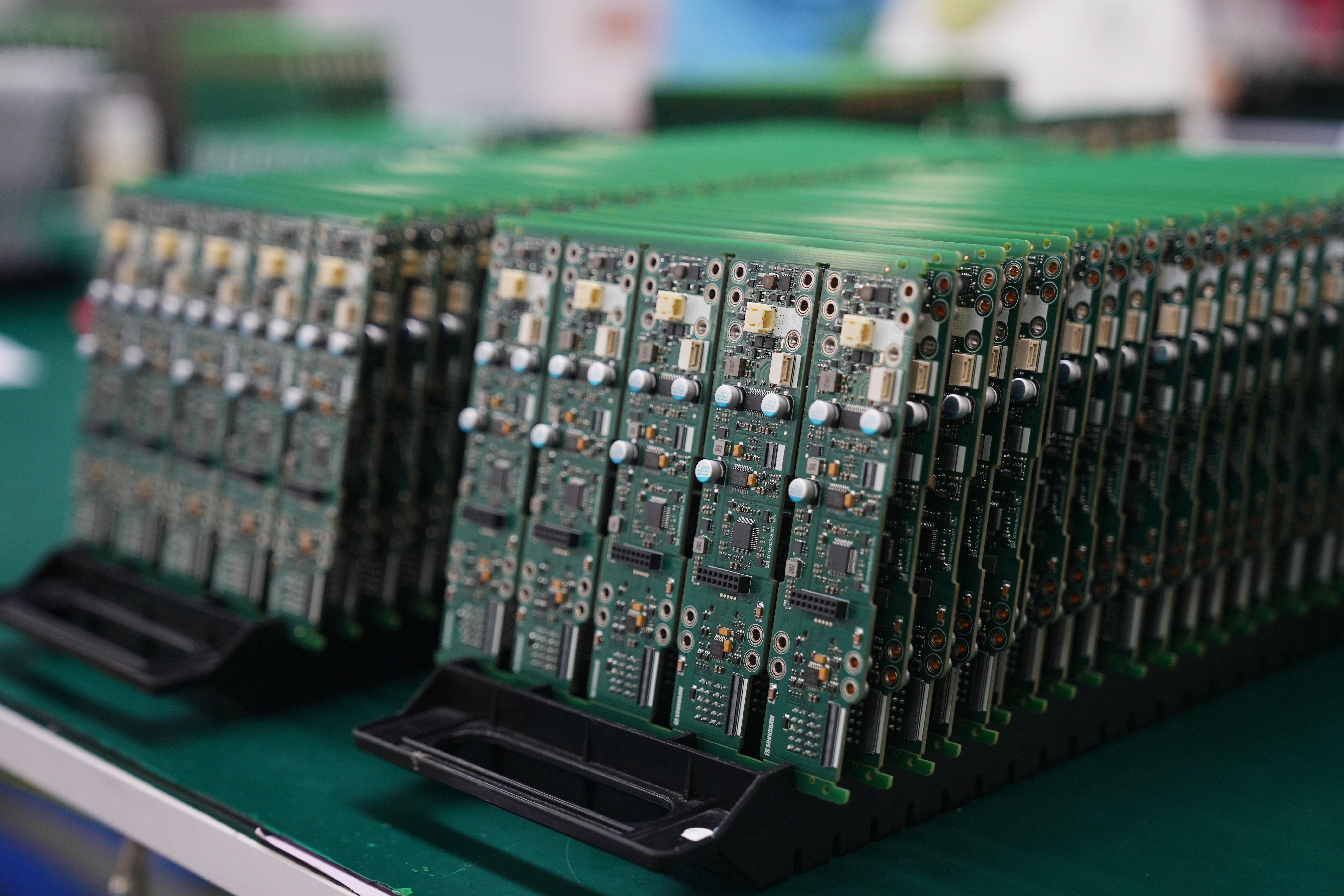
- Quality Control & Rapid Response: Full-process monitoring and S-parameter/eye-diagram testing ensure batch-to-batch high-frequency parameter deviation <±1%. Samples in 7 days, mass production in 15 days, with 98% on-time delivery rate.
Welcome to contact us if you have any request for RF amplifier PCB design and assembly: sales@bestpcbs.com.
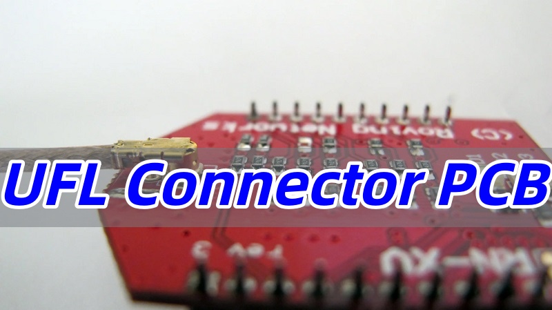
What Is A RF Amplifier PCB?
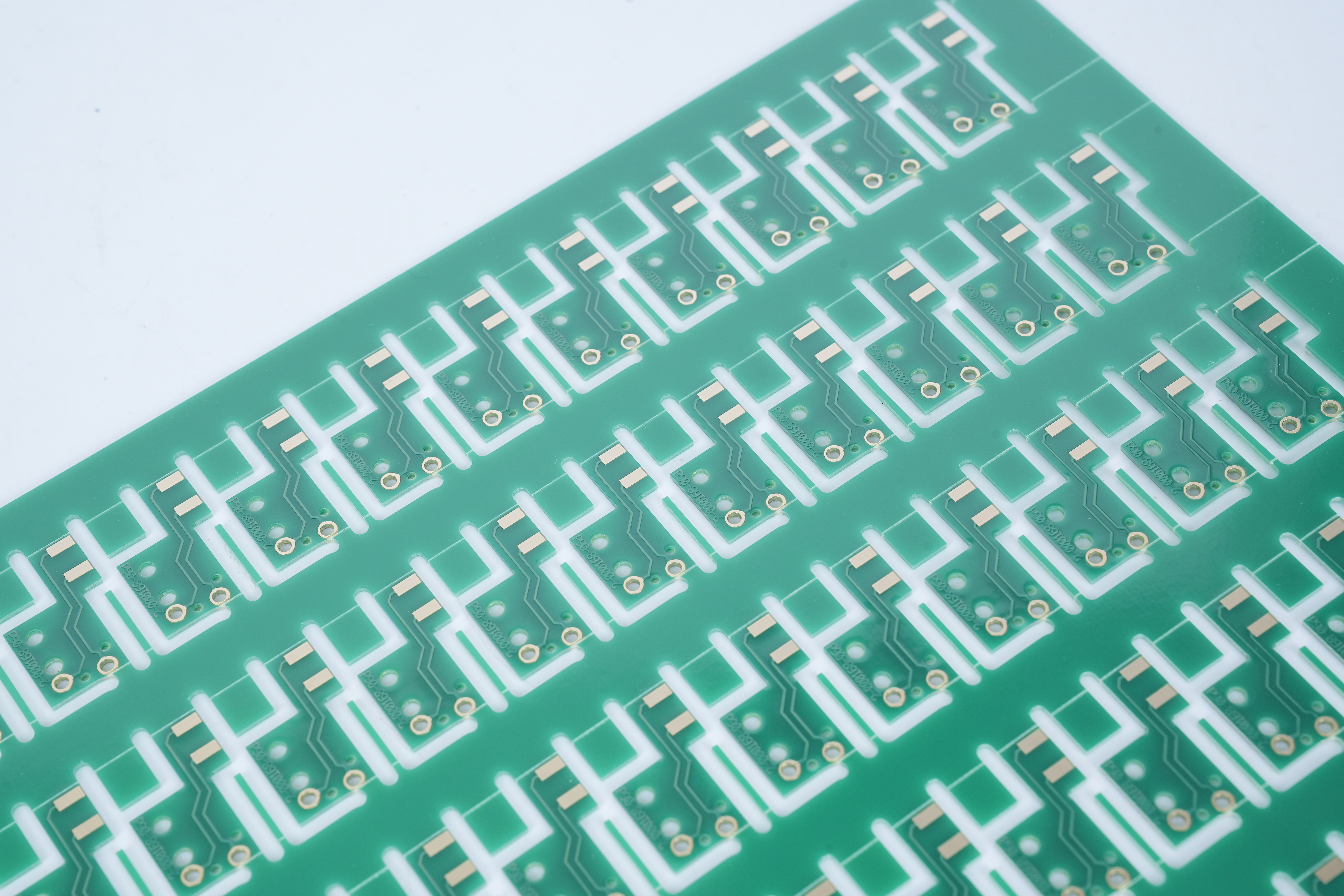
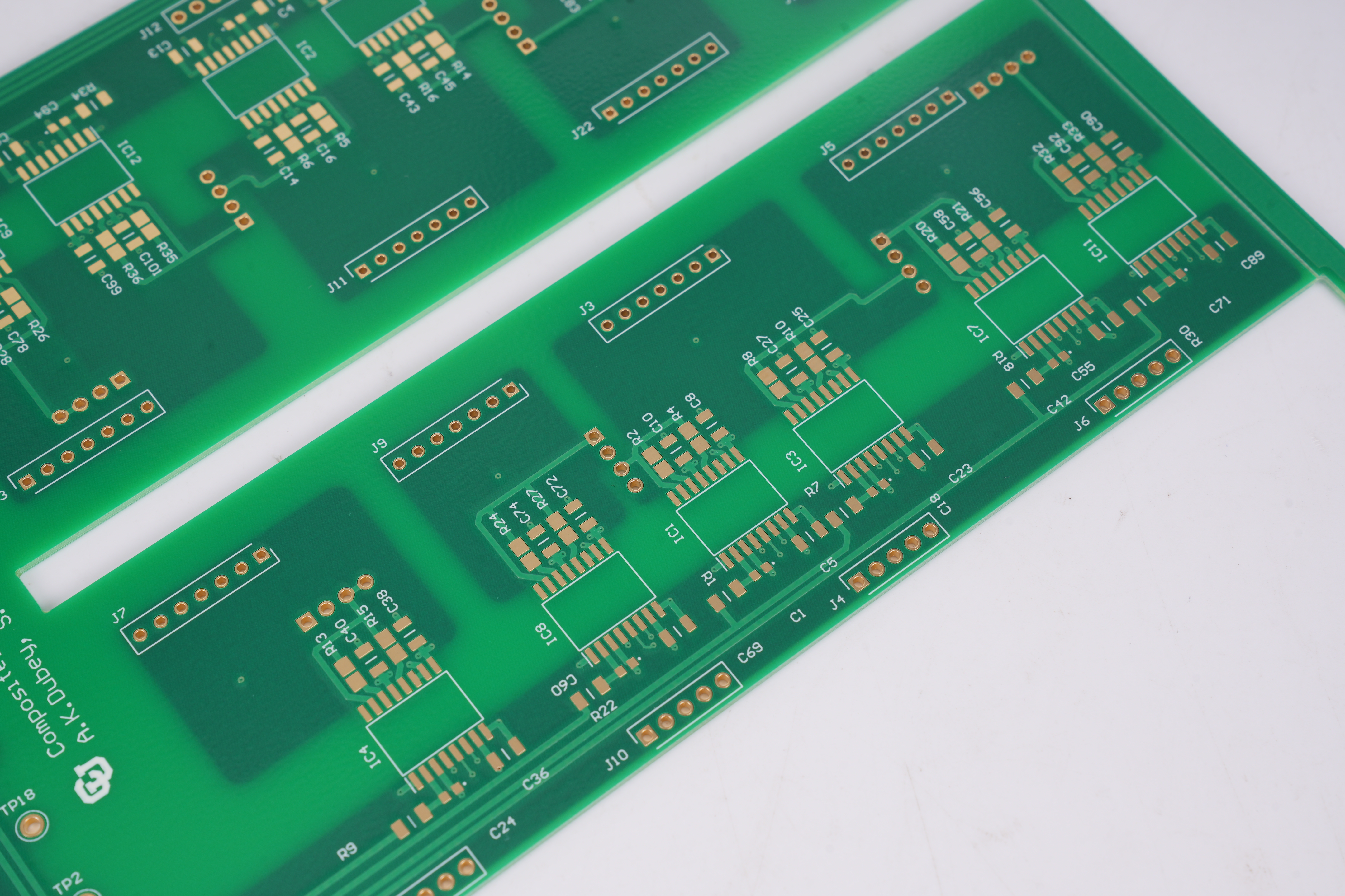
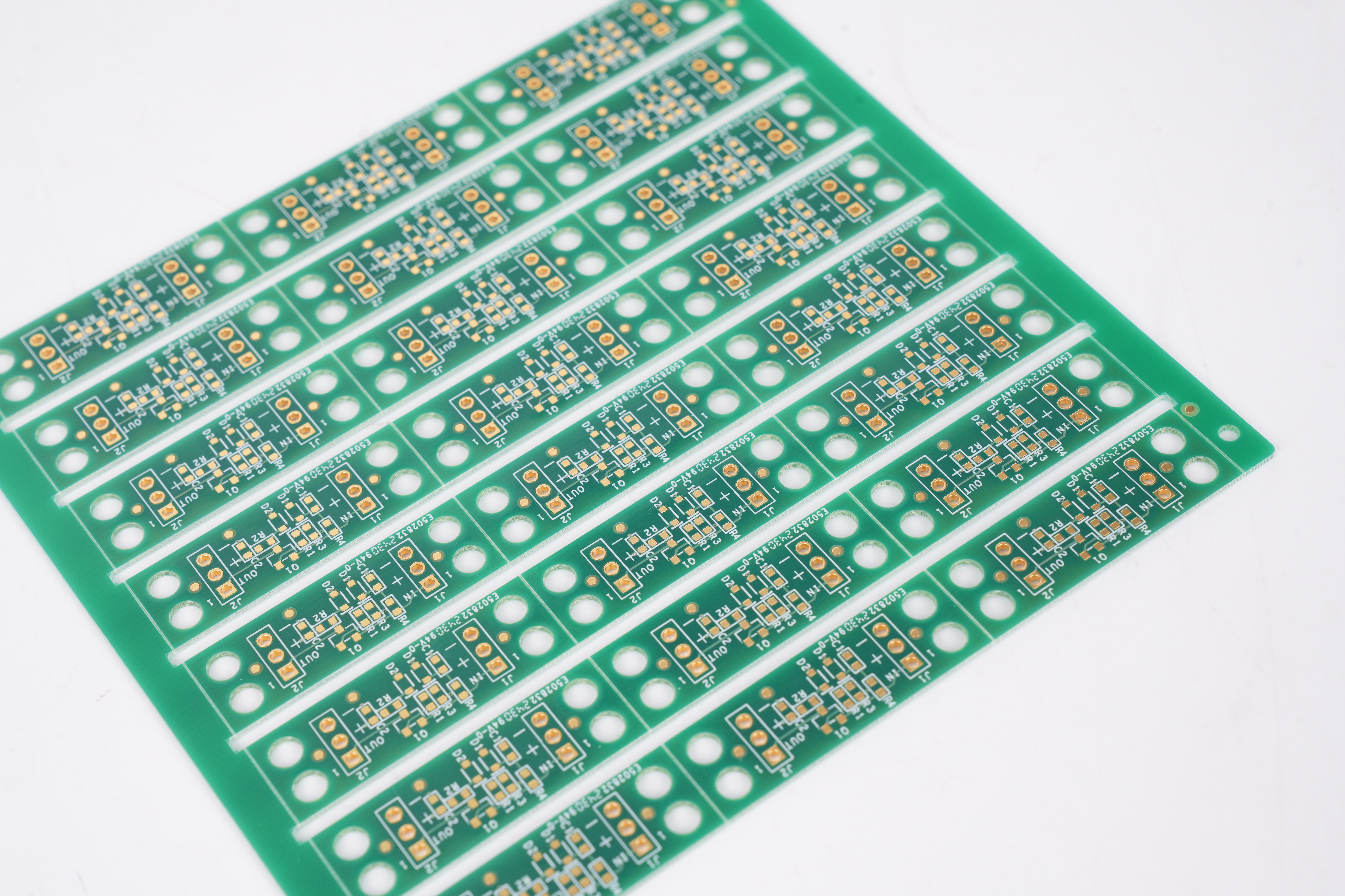
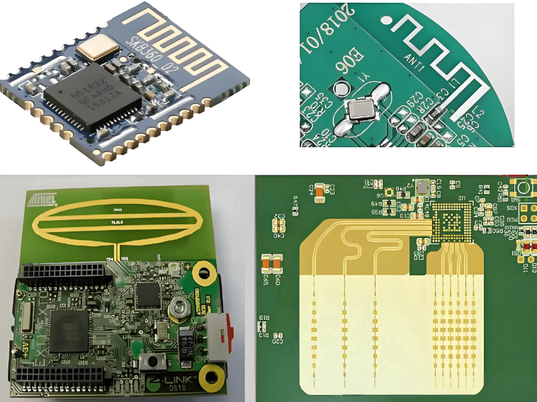
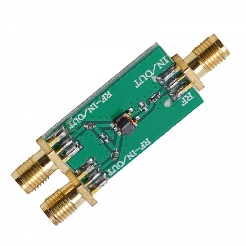
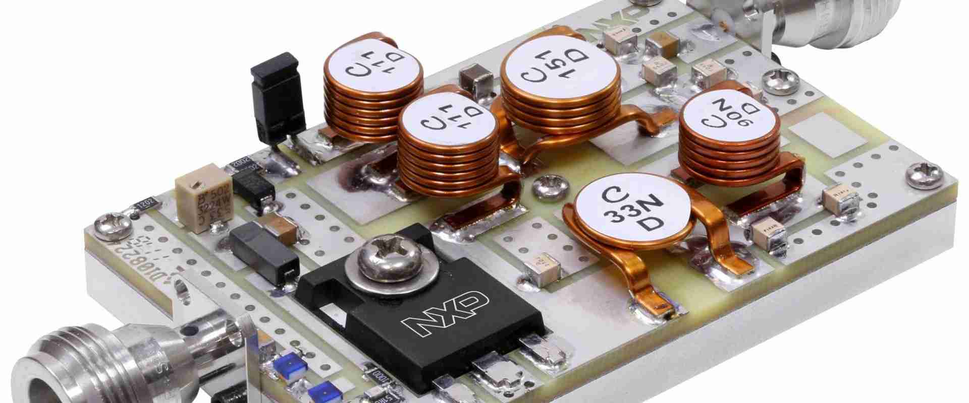
A RF amplifier PCB is a circuit board created to support amplification stages that work in radio-frequency ranges. It carries components such as low-noise amplifiers, gain blocks, filters, bias circuits, and matching networks. Since RF energy reacts to small layout changes, the board must control impedance, grounding, and routing with more care than general PCBs. Furthermore, material choice, stack-up, and copper patterns influence how signals move through each trace. When these factors align, the amplifier remains stable, gains remain predictable, and unwanted radiation stays low.
What Are Types of RF Amplifier PCBs?
- Low-Noise Amplifier (LNA) PCB: These boards serve front-end systems in radios, satellite receivers, and radar sensors. Their goal is to lift micro-level input signals with very low added noise. LNAs rely on controlled impedance, a short input path, and a clean ground to reduce noise figure.
- Power Amplifier (PA) PCB: PA boards push RF energy to a much higher level. They appear in transmitters, cellular base stations, industrial heating systems, and radar emitters. Because of higher current, these boards need thick copper, thermal relief paths, and stable bias networks.
- Driver Amplifier PCB: A driver board takes medium-level signals and prepares them for a PA stage. It must handle some power while still keeping reasonable linearity.
What Are Applications of RF Amplifier PCB Board?
- 5G, LTE, and Wi-Fi systems in mobile devices and base stations.
- Radar sensors used in autonomous driving, drones, and traffic monitoring.
- Satellite communications for navigation, broadcasting, and remote sensing.
- IoT nodes that need compact front-end amplification.
- Test and measurement devices such as spectrum analyzers and signal generators.
- Medical imaging and diagnostic tools that involve RF detection stages.
- Industrial RF heating and plasma equipment.
RF Amplifier PCB Design Technical Parameter
| Parameter | Typical Specification |
| Operating Frequency Range | 0.5–6 GHz |
| Gain | 20±1 dB @ 25°C |
| Noise Figure (NF) | ≤1.2 dB (LNA) / N/A (PA) |
| Output Power (Pout) | 30 dBm (PA) / 10 dBm (Driver) |
| Output Third-Order Intercept Point (OIP3) | +40 dBm |
| Voltage Standing Wave Ratio (VSWR) | ≤1.5:1 (Input/Output) |
| Operating Voltage | +5V DC, ±10% |
| Operating Current | 120 mA (LNA) / 800 mA (PA) |
| Power Added Efficiency (PAE) | >45% (PA) |
| PCB Substrate | Rogers 4350B/Taconic RF-35/FR4-HF |
| Copper Thickness | 1–2 oz (35–70 μm) |
| Impedance Control Accuracy | 50Ω ±5% |
| Layer Count | 2–8 layers |
| Thermal Resistance (θja) | ≤15°C/W (PA with Heatsink) |
| Operating Temperature | -40℃ ~ +85℃ |
| Storage Temperature | -55℃ ~ +125℃ |
| Humidity Tolerance | 95% Non-condensing |
| EMC Standards | FCC Part 15, CE, RoHS 3 |
| Lead-free Process | Compliant (Sn96.5/Ag3.0/Cu0.5) |
| Mean Time Between Failures (MTBF) | >100,000 hours |
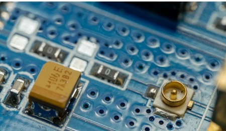
| I/O Interfaces | SMA/QMA/MMCX/Solder Pads |
| Shielding Enclosure | Optional EMI Shielding Case |
| Test Points | Integrated VNA Calibration Test Points |
RF Amplifier PCB Design Guideline
A detailed guideline to RF amplifier PCB design:
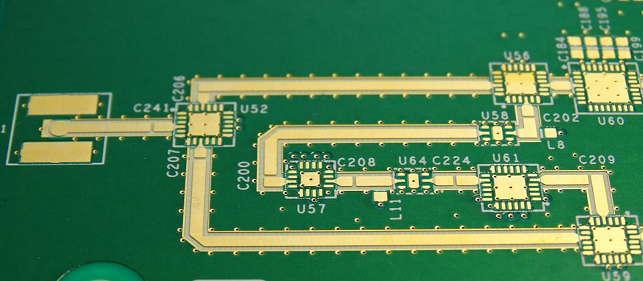
1. Layout Partitioning and Isolation Design
- Mixed-signal isolation: Strictly separate analog, digital, and RF zones. Maintain minimum spacing of 10mm (≥20mm for high-frequency applications) between digital circuits and RF sections to prevent cross-coupling. Implement “star” power routing to minimize noise crosstalk. Position sensitive components (e.g., LNAs, mixers) close to antennas or RF ports to reduce path length and losses.
- Shielding and grounding: Use via fences (spacing ≤λ/20) to construct isolation bands. Install metal shielding enclosures (e.g., copper cavities) in sensitive areas. Ensure continuous ground planes without segmentation. Recommend dual-layer grounding with via stitching (spacing ≤λ/10) to enhance EMI protection.
2. Impedance Control and Transmission Line Design
- Material selection: For frequencies above 1GHz, prioritize low-loss substrates (e.g., Rogers RO4350B, Taconic RF-35) over traditional FR4 (loss tangent 0.02-0.025). Materials must meet stable dielectric constant (Dk: 3.48±0.05@10GHz) and low moisture absorption (<0.1%).
- Impedance matching: Transmission line characteristic impedance must precisely match standards (e.g., 50Ω). Use microstrip/stripline structures and avoid 90° bends; adopt 45° miters or curved transitions. Validate stackup designs with field solvers (e.g., Polar Si8000) to maintain <±10% impedance tolerance.
3. Power and Thermal Management
- Decoupling and filtering: Deploy multi-stage filtering (LC/π networks) at power entry points. Place small-value (0.1μF) ceramic capacitors near ICs combined with bulk (10μF) electrolytic capacitors in “star” topology to reduce IR drops.
- Thermal design: Under high-power devices (e.g., PAs), implement thermal via arrays filled with conductive adhesive. Integrate heat sinks or metal-core substrates (e.g., aluminum) to enhance heat dissipation, ensuring junction temperature remains below 125°C.
4. Signal Integrity and EMC Protection
- Routing rules: Avoid cross-layer via transitions for RF signal lines. When necessary, use via-in-pad or back-drilling to eliminate stubs. Maintain ≥3× line width spacing between high-speed digital signals and RF traces, or employ differential pairs for balanced transmission.
- EMI suppression: Install ground traces along board edges and common-mode chokes at critical interfaces. Optimize layouts through simulation (ADS/HFSS) and ensure compliance with FCC/CE radiation limits (e.g., EN55022).
5. Manufacturing and Testability Design
- Process specifications: Adhere to IPC-6012 standards. Define minimum trace width/spacing compatible with manufacturing capabilities (e.g., 100μm for HDI processes). Specify stackup details including layer thickness, copper weight, and solder mask dimensions.
- Test validation: Include test points (e.g., SMA connectors) and debugging pads. Deploy temperature rise monitoring at critical nodes. Verify S-parameters (e.g., S21, S11) with network analyzers to confirm gain and noise figure specifications.
6. Documentation and Regulatory Compliance
- Design documentation: Provide complete BOM, Gerber files, stackup reports, and simulation models. Annotate critical parameters (Dk/Df values, thermal resistance curves) with international certifications (UL, RoHS).
- Regulatory adaptation: Configure power filtering solutions to meet regional standards (e.g., IEC 61000-4-2 ESD requirements for EU/NA markets).
RF Amplifier PCB Layout Technique
Below are some techniques of RF amplifier PCB layout for your reference:
Signal Flow and Layout Planning
- Linear Layout Principle: Arrange the main signal path in a “linear” configuration within the shielding cavity, avoiding U-shaped or complex paths to minimize self-interference. Use L-shaped layouts when space is constrained. Multi-channel systems require fully symmetric layouts to ensure phase consistency.
- Functional Partition Isolation: Isolate digital, analog, and RF circuits physically. High-Power Amplifiers (HPA) and Low-Noise Amplifiers (LNA) must be separated by ≥5mm or placed on different layers. Use cavity isolation for sensitive circuits and strong radiation sources, and add shielding between multi-stage amplifier stages.
Ground System Design
- Grounding Method Selection: Single-point grounding for low-frequency control signals; multi-point grounding (via spacing ≤λ/20) for high-frequency RF signals. Partition ground layers by function (RF, digital, power) and connect them at a single point.
- Ground Via Arrays: Place ground vias on both sides of RF microstrip lines (spacing 0.5-1mm) to form an electromagnetic barrier. Ensure shielding cavity bottom grounding impedance ≤0.1Ω to avoid secondary radiation.
Power Decoupling and Filtering
- Star Power Routing: Use a star configuration for power networks. Parallel large capacitors (e.g., 10μF electrolytic) and small capacitors (0.1μF MLCC) at the root node to extend the frequency band. Place capacitors close to power pins and connect ground terminals via short leads to the ground plane.
- Pi-Type Filter: Add a pi-type filter (series RFC with impedance ≥1kΩ@operating frequency + parallel capacitor) at the power input to suppress high-frequency noise. Example: Adding a pi-type filter to a 10W PA power terminal reduces ripple from 200mV to 10mV.
Signal Routing and Impedance Control
- 50Ω Impedance Design: RF signal line width ≥15mil. Use cross-layer references to ensure stable impedance. Use rounded corners instead of right angles. Maintain a 2W spacing (minimum 1W) between RF traces and ground copper.
- Sensitive Signal Isolation: Keep analog small signals away from high-speed digital and RF signals. Maintain a clearance of ≥5mm in all layers for antenna areas to reduce interference.
Thermal Management and Heat Dissipation
- Heat Dissipation Solutions: Use copper/aluminum heat sinks for high-power amplifiers, combined with natural convection or forced air cooling. Use liquid cooling/heat pipes in extreme cases. Fill the gap between the chip and the heat sink with thermal grease or phase-change material to reduce thermal resistance.
- Thermal Vias and Copper Layers: Add thermal vias, thicken copper layers, optimize the layout of high-heat components, and avoid clustering heat-sensitive areas. Integrate temperature sensors to trigger over-temperature protection.
Electromagnetic Compatibility and Shielding
- Metal Shielding Cavity: Enclose high-power amplifiers in aluminum/brass shielding cavities (thickness 0.2-0.5mm) with grounding impedance ≤0.1Ω. Add ventilation holes (diameter ≤λ/20) or attach heat sinks to the top.
- Filtering Techniques: Use pi-type or LC filters on power and signal lines to suppress conducted and radiated interference. Add series resistors/magnetic beads to control signal lines and attenuators to RF test points.
Why Partner With EBest Circuit (Best Technology) for RF Amplifier PCB Manufacturer?
Reasons why choose EBest Circuit (Best Technology) for RF amplifier PCB manufacturer:
- Global Certification Standards Compliance: Certifications include ISO 9001 quality management, IATF 16949 automotive standards, medical-grade ISO 13485, and RoHS environmental compliance. These certifications meet high-standard requirements across consumer electronics, automotive, medical, and global market access conditions.
- 19 Years of Industry Expertise: With 19 years of specialized experience in RF PCB manufacturing and over 5,000 successful projects, expertise includes high-frequency substrate processing, microstrip impedance control, and thermal optimization. This experience enables rapid identification and resolution of design-related manufacturing risks.
- Free DFM Manufacturability Analysis: Senior engineering teams provide free DFM analysis to proactively identify manufacturability issues such as overly small trace widths, spacing, or pad design flaws. This reduces redesign costs, shortens time-to-market, and improves mass production yield.
- Competitive Pricing with Cost-Sensitive Design Solutions: Leverage economies of scale and process optimization to deliver market-leading quotes. Customize cost-sensitive solutions tailored to client designs, such as alternative high-performance materials or streamlined production flows, directly reducing manufacturing costs by 30%-50% for budget-sensitive RF amplifier projects.
- 24-Hour Rapid Prototyping for Urgent Orders: Dedicated rapid-response teams enable 24-hour turnaround from order placement to sample delivery. Parallel engineering processes and pre-stocked material libraries ensure R&D timelines remain unaffected, helping clients seize market opportunities ahead of competitors.
- 99.2% On-Time Delivery Rate: Intelligent production scheduling systems and real-time supply chain monitoring achieve end-to-end process visibility. Historical data confirms a 99.2% on-time delivery rate, significantly exceeding industry averages and ensuring stable client production planning.
- Batch Production Full Inspection and Rigorous Quality Control: Each production batch undergoes 100% inspection via AOI optical testing, X-ray layer inspection, and electrical performance verification. Combined with SPC statistical process control, key RF parameters like gain and noise figure maintain consistency, with defect rates controlled below 0.08%.
- Flexible Production Scalability: Automated production lines support full lifecycle services from prototyping to mass production. Capability to rapidly adjust capacity accommodates small-batch trial production to high-volume orders, avoiding overcapacity risks while ensuring seamless transitions between production scales.
Feel free to contact us at sales@bestpcbs.com if you have any inquiry for RF amplifier PCB design, production and assembly.
Common FAQs to Avoid in RF Amplifier PCB Design
Q1: Why does a poor ground system cause instability in an RF amplifier PCB?
A1: weak ground system raises return-path impedance and increases the chance of unintended coupling. When the RF return path does not flow under its matching trace, the loop grows larger and the amplifier becomes sensitive to noise and oscillation. Using a solid ground plane and many stitching vias shortens the loop and keeps the board stable at high frequency.
Q2: What happens if RF traces are longer than necessary?
A2: Long traces add loss, increase parasitic inductance, and create phase shifts that distort gain. They also pick up more noise from nearby circuits. RF input traces should be as short and direct as possible. Shorter routing keeps the amplifier’s noise figure low and preserves signal strength.
Q3. Why is placing matching networks far from the device a common mistake?
A3: Matching networks work only when placed close to amplifier pins. If they sit too far away, the trace between the device and matching parts becomes part of the matching network itself. This shifts impedance, raises reflection, and weakens overall gain. Keeping these components close maintains predictable matching.
Q4: What risk appears when digital and RF circuits are not isolated?
A4: Digital circuits generate sharp edges that spread electromagnetic noise. When digital zones sit near RF paths, this noise couples into the amplifier stage, causing ripple, distortion, and reduced sensitivity. Placing digital, RF, and power areas separately lowers interference and supports smoother performance.
Q5: Why does ignoring thermal relief cause failures in power RF amplifiers?
A5: Power amplifiers release heat during normal operation. If the board lacks enough copper area, thermal vias, or heat-spreading design, temperature rises quickly and shifts gain, bias, or linearity. In severe cases, the device may degrade. Good thermal planning keeps temperature stable and extends the amplifier’s usable life.