A 0.1nh smd inductor is a passive surface-mount component with an exceptionally low inductance of 0.1 nanohenries, primarily used to manage and fine-tune signal integrity in ultra-high-frequency (UHF) and microwave circuits. This article will demystify this tiny component, explain its critical role, and illustrate why expert PCB fabrication and assembly are paramount for its successful implementation.
Designing circuits that utilize components like a 0.1nh smd inductor presents unique engineering and manufacturing challenges. Have you ever faced these common frustrations?
- Parasitic Overwhelm: Stray capacitance and inductance from the PCB itself can easily exceed the target 0.1 nh inductor value, rendering the component ineffective.
- Inconsistent Performance: Minor variations in solder paste volume or placement accuracy during SMT can drastically alter the final inductance, causing circuit failure.
- Measurement Headaches: Accurately measure nh inductor values, especially in-circuit, requires specialized equipment and techniques not commonly available.
- Identification Difficulties: Physically how to identify smd inductor components and verify their smd inductor values without clear marking is a constant hassle.
- Supplier Reliability Issues: Sourcing genuine, high-precision components like a 0.1nh smd inductor 0402 metric part from unreliable channels leads to project delays and quality risks.
These challenges highlight that the board is an integral part of the component itself. The solution lies in partnering with a manufacturer whose expertise extends beyond simple assembly to encompass holistic, high-frequency design support.
- Mitigating Parasitics: We employ advanced simulation and modeling to design PCB layouts (trace geometry, ground planes, layer stack-up) that minimize parasitic effects, ensuring the 0.1nh smd inductor performs as intended.
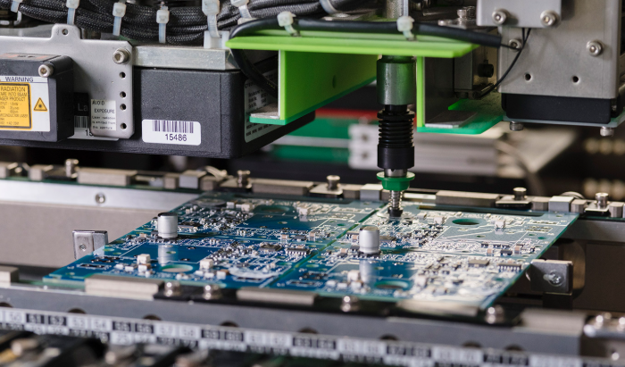
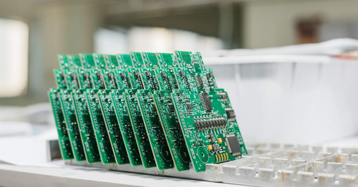
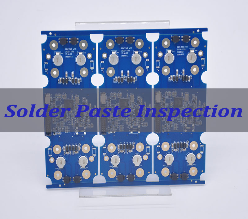
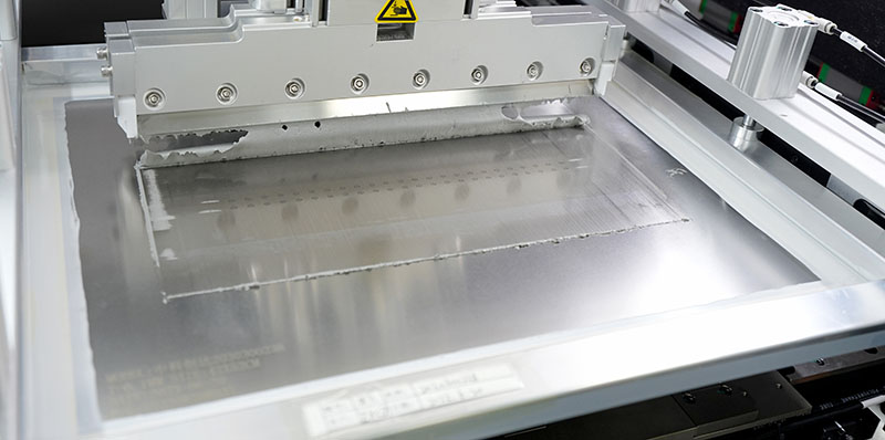
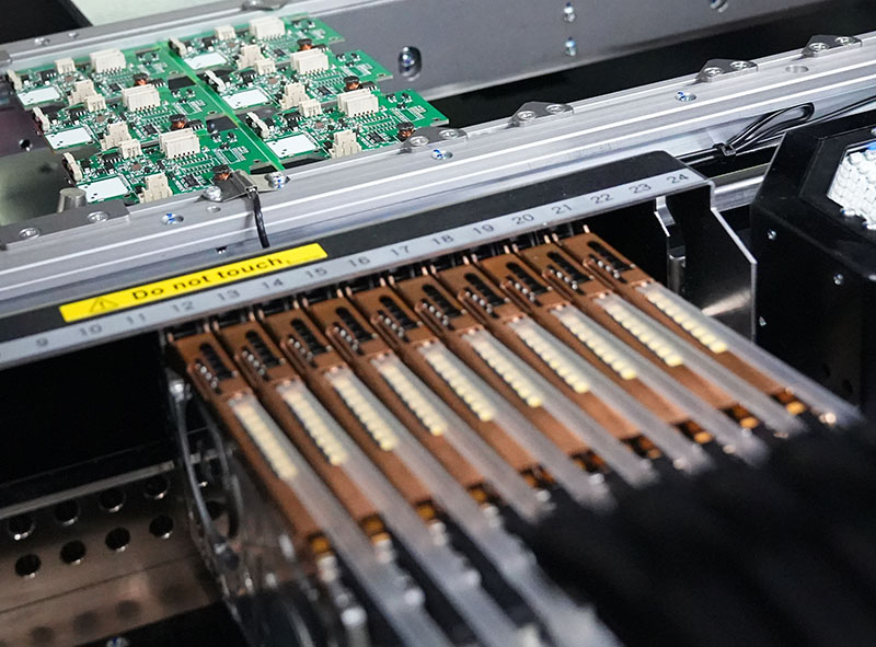
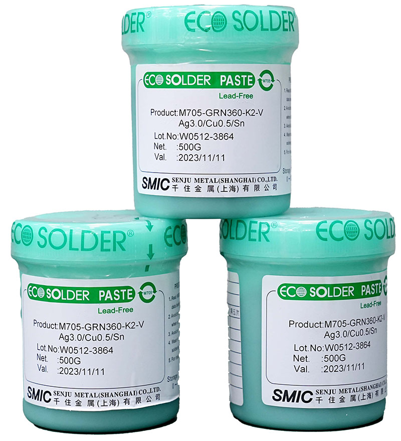
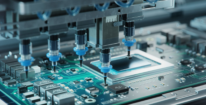
- Ensuring Process Precision: Our controlled SMT lines with fine-paste printing and high-accuracy chip shooters guarantee consistent placement and soldering, preserving the delicate electrical characteristics of ultra-low inductor nh components.
- Providing Validation Support: We offer guidance on proper measurement techniques and, where needed, can provide test data to verify that the as-assembled NH inductor performance meets specifications.
- Aiding in Component Management: We assist in supply chain management and component verification, ensuring you receive authentic parts, reducing the burden to identify SMD inductor components incorrectly.
- Leveraging Proven Expertise: Our experience with RF/microwave projects means we understand the criticality of every 0.5nh inductor or 1nh inductor choice and can advise on design for manufacturability from the start.
At BEST Technology, we are a professional PCBA manufacturer with deep expertise in RF and high-speed digital circuits. We combine state-of-the-art PCB fabrication—including specialized materials for high-frequency applications—with precision SMT assembly to ensure that sensitive components like the 0.1 nh inductor realize their full potential on your board. For projects where every picobenry counts, partner with us. Pls feel free to contact our team at sales@bestpcbs.com to discuss your requirements.
What is a 0.1nh SMD Inductor?
A 0.1 nanohenry (nH) Surface-Mount Device (SMD) inductor is one of the smallest practical inductance values available. It acts as a tiny reservoir for magnetic energy, presenting minimal impedance to low-frequency or DC signals but increasing impedance as frequency rises. Its primary role is not energy storage but fine-tuning and parasitic compensation in very high-speed scenarios.
- Physical Scale: It is extremely small, often in an 0402 metric (0.5mm x 0.25mm) or even 0201 package.
- Core Function: To provide a precise, negligible series inductance for impedance matching, RF choke applications in GHz ranges, or to cancel out unwanted parasitic capacitances.
- Construction: Typically a single air-core or ceramic-core loop of wire, as any magnetic core material would introduce excessive loss and variability at these frequencies.
- Key Characteristic: Its inductor nh rating is so low that the parasitic inductance of its PCB pads and connecting traces must be meticulously controlled.
In summary, the 0.1nh smd inductor is a precision tuning element for the highest echelons of circuit design, where its value is dwarfed by the inductance of a few millimeters of PCB trace.

What Is the Difference Between a 0.1mH Inductor and a 0.1nH Inductor?
The difference is vast—one million times (1,000,000x) in value. “mH” stands for millihenry, and “nH” for nanohenry.
- Magnitude: 1 mH = 1,000,000 nH. Therefore, a 0.1 mh inductor (0.1 mH) is equal to 100,000 nH, which is one million times larger than a 0.1 nh inductor (0.1 nH).
- Application Spectrum:
| Feature | 0.1 mH Inductor | 0.1 nH Inductor |
|---|---|---|
| Typical Use | Power filtering, low-frequency chokes | RF matching, UHF/Microwave circuits |
| Frequency Range | kHz to low MHz | GHz and above |
| Physical Size | Relatively large | Extremely small (0402, 0201) |
| Core Concern | Current handling, saturation | Parasitic effects, PCB layout |
- Design Impact: Using a 0.1mh inductor where a 0.1nh is needed would completely block high-frequency signals. Conversely, using a 0.1nH where 0.1mH is required would provide no filtering effect at all.
In essence, they belong to different worlds of electronics: one for energy and low-frequency signals, the other for controlling the behavior of radio waves and ultra-fast digital edges.
What is the Color Code of 0.1 MH Inductor?
Through-hole inductors with values like 0.1 mh inductor sometimes use a color band system similar to resistors to denote their value in microhenries (µH).
For a 0.1 mH (which is 100 µH) inductor, a common color code would be: Brown (1), Black (0), Brown (x10), and often a fourth band for tolerance (e.g., Silver for ±10%).
This represents 10 x 10 = 100 µH. It is crucial to note that SMD inductors, especially tiny ones like a 0.1nH type, almost never use color codes. They are typically marked with a numeric or alphanumeric code, if marked at all, due to their minuscule size.
How to Identify SMD Inductor?
How to identify smd inductor components amidst other similar-looking SMD parts (like capacitors or resistors) involves a multi-step approach:
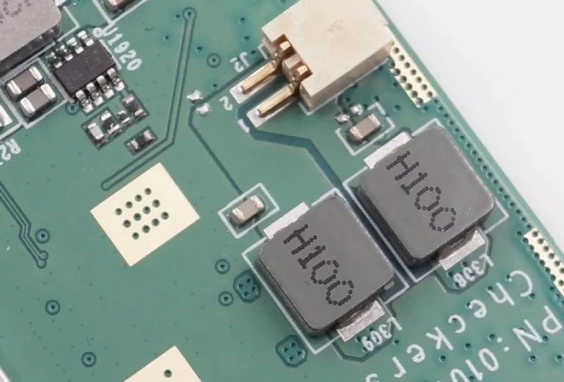
- Consult the PCB Schematic & BOM: The definitive source. The designator (usually “L” for inductor) and listed value are your first reference.
- Check the Board Silkscreen: The “L” designator printed on the PCB next to the component.
- Look for Markings: Some larger SMD inductors have a numeric code. A “100” might mean 10 µH, “1R0” is 1.0 µH. For values below 1 µH, “R” indicates a decimal point (e.g., “R10” = 0.10 µH = 100 nH). A 0.1nh smd inductor is often unmarked.
- Visual Inspection: Inductors may have a dark ceramic or beige body, sometimes with visible wire coils on larger models. They are distinct from multilayer ceramic capacitors (MLCCs) which are typically light beige/brown with a smooth surface.
- Electrical Measurement (Off-Board): Using an LCR meter is the most reliable method to determine smd inductor values. This is essential for unmarked or suspect components.
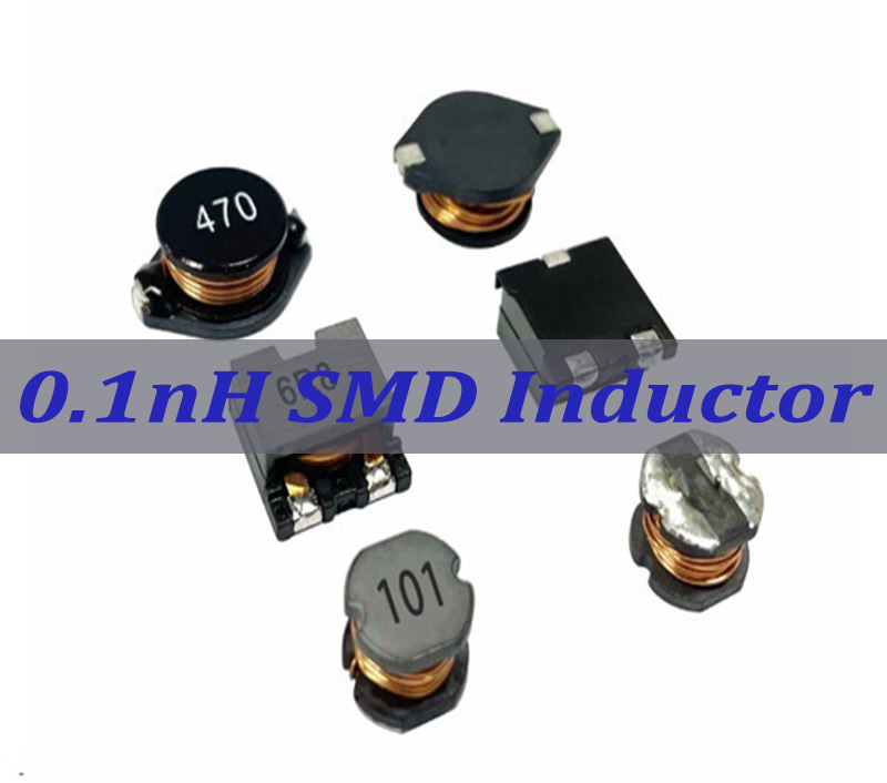
What Does a 0.1nh SMD Inductor 0402 Metric Package Look Like?
A 0.1nh smd inductor 0402 metric package is nearly indistinguishable from a 0402 resistor or capacitor to the naked eye.
- Dimensions: It measures approximately 1.0mm x 0.5mm in imperial naming, or more precisely 0.5mm x 0.25mm (length x width) in the metric system.
- Appearance: It is a tiny, rectangular ceramic or composite block. The body color is often a dark gray, black, or sometimes beige.
- Terminations: It has two metallic electrodes (usually solder-coated) on each end. For such a low value, it is essentially a straight piece of thick wire or a single-turn loop molded into the chip, so there are no visible windings.
- Markings: It frequently has no markings at all due to its minute size. When present, a simple code like “0R1” (for 0.1 nH) might be used, but this is rare.
How to Find SMD Inductor Value?
To find or verify smd inductor values, follow this hierarchy:
- Design Documentation (BOM/ Schematic): Always the first and most accurate source.
- Component Packaging/Reel Label: The tape-and-reel or bag label from the manufacturer will specify the part number and value.
- Decode Markings: Use the manufacturer’s datasheet to interpret any printed alphanumeric codes.
- Measure with an LCR Meter: For unmarked components or verification, this is essential.
- Crucial: You must measure nh inductor values off the board to avoid parallel/series parasitic effects from the circuit.
- Use the meter’s appropriate test frequency (often 1 MHz or higher for nH-range inductors).
- Network Analyzer (In-Circuit): For the highest accuracy, especially for values like 0.5nh inductor or 1nh inductor, a vector network analyzer (VNA) can measure the component’s effect in situ.
What Determines SMD Inductor Values in RF and High-Speed Circuits?
In sensitive RF and high-speed designs, the effective SMD inductor values are not just determined by the component itself but by the entire implementation.
- Component Design: The number of turns, coil diameter, core material (if any), and internal construction.
- PCB Layout (Parasitics): This is the dominant external factor. Trace length, width, proximity to ground planes, and via stubs add series inductance and parallel capacitance.
- SMT Assembly Quality: Solder fillet size and shape change the current path and thus the inductance. Excess solder can create a shorting blob; too little can increase parasitic resistance.
- Grounding & Return Path: The inductance of the return current path is part of the total loop inductance.
- Adjacent Components: Coupling to nearby traces or components can alter the effective inductance.
Therefore, achieving a precise 0.1 nh inductor performance requires designing the PCB and process as part of the component itself—this is where Advanced PCB and SMT Expertise becomes critical.
How to Measure NH Inductor?
Accurately measuring an NH inductor, such as a 0.5nh inductor or 0.1nh smd inductor, is challenging due to the influence of test fixtures.
- Use a Quality LCR Meter or Impedance Analyzer: Ensure it has a resolution down to the nH range and supports high test frequencies (≥ 1 MHz).
- Employ a Short-Open-Load-Through (SOLT) Calibration: Use calibration standards for your test fixture to negate the fixture’s own parasitics. This is mandatory for meaningful nH measurements.
- Use Dedicated SMD Test Clips or a Probe Station: These minimize added lead inductance. Never use long wires.
- Measure at the Relevant Frequency: Inductance can vary with frequency. Measure at or near your circuit’s operating frequency.
- Understand the Limitations: For values below 1 nH, even the best bench-top methods have significant relative error. Production testing often uses a “go/no-go” comparative method against a known gold standard.
What Are SMD Inductor Used For?
SMD inductors are ubiquitous in modern electronics. Their uses span from power management to RF, with the value dictating the application:
- Power Supplies: Larger values (µH to mH) are used in DC-DC converter output filters (LC circuits) to smooth current.
- RF & Microwave Circuits: Mid-range (nH to low µH) and ultra-low values (0.1nh inductor, 0.5nh inductor) are used for:
- Impedance matching networks.
- RF chokes (to block RF while passing DC).
- Resonant tank circuits in oscillators and filters.
- Inductor nh ratings are chosen for specific GHz-frequency operations.
- High-Speed Digital: Very low nH inductors are used in series termination to dampen ringing without excessively slowing the edge rate.
- Signal Filtering: Forming LC filters to block unwanted noise frequencies.
Why Do Engineers Select an Inductor NH Rating for Ultra-High-Frequency Designs?
Engineers select specific inductor nh ratings in UHF designs primarily for resonance and impedance control.
- Creating Resonance: The formula
f_resonance = 1 / (2π√(LC))shows that at GHz frequencies, achieving resonance requires picofarad (pF) capacitors and nanohenry (nH) inductors. A 1nh inductor with a 2.5pF capacitor resonates at about 3.2 GHz. - Precise Impedance Matching: At these frequencies, transmission lines and component inputs/outputs have specific impedances (e.g., 50Ω). Tiny nH-range inductors are used in matching networks (with capacitors) to transform impedances and maximize power transfer, minimizing signal reflection.
- Parasitic Cancellation: Unwanted stray capacitance (a few pF) can be “tuned out” by adding a series or parallel inductor of a complementary nH value.
- Controlled Reactance: The inductive reactance (
XL = 2πfL) at, say, 10 GHz for a 0.1nh smd inductor is only about 6.3Ω. This allows for fine, minimal-impact adjustments to a circuit’s phase or impedance.
When Should You Use a 0.5nH Inductor Instead of a 0.1nH SMD Inductor?
The choice between a 0.5nh inductor and a 0.1nh smd inductor is a matter of precise circuit tuning, dictated by the target frequency and the surrounding parasitics.
- Lower Target Frequency / Higher Capacitance: If your matching network or resonator uses a larger capacitor value, you will need a larger inductor to achieve the same resonant frequency (
L ∝ 1/Cfor a fixed f). - Compensating for Larger Parasitic Inductance: If the PCB layout or package introduces more series parasitic inductance than anticipated, you might need to reducethe value of the discrete inductor (e.g., use 0.1nh instead of a planned 0.5nH) to hit the total inductance target.
- Achieving a Specific Reactance: For a given frequency, a 0.5nh inductor provides five times the inductive reactance of a 0.1nh one. If a circuit node requires a specific impedance, the required
Lvalue is calculated directly fromXL = 2πfL. - Practical Availability and PCB Real Estate: Sometimes, the calculated ideal value (e.g., 0.23 nH) isn’t available. An engineer might choose a 0.2nH or 0.5nH standard value and tweak the companion capacitor instead.
Why Choosing the Right PCBA Manufacturer Matters for a 0.1nH SMD Inductor?
Implementing a 0.1nh SMD inductor successfully is less about the component and more about its environment. The wrong manufacturing partner can nullify your careful design.
- Parasitic Control: Only a manufacturer skilled in RF layout understands how to design traces and grounding to avoid adding stray inductance that swamps the 0.1 nH value.
- Material Selection: High-frequency board materials (like Rogers) with stable Dk/Df are often needed, which not all fabricators handle routinely.
- Process Control: SMT process variation is the enemy of ultra-low inductor nh stability. Precision stencil design, paste control, and placement accuracy are non-negotiable.
- Design for Manufacturing (DFM) Review: An expert manufacturer will identify layout features that could degrade performance before the board is built.
- Testing and Validation: They should have the capability and knowledge to verify high-frequency performance, ensuring the assembled board meets your specs.
Choosing a partner like BEST Technology, with Advanced PCB and SMT Expertise, ensures that your high-frequency design intent is faithfully and reliably translated into a working product.
To conclude, the 0.1nh smd inductor is a critical, precision component that enables the function of ultra-high-frequency and high-speed digital circuits by providing minuscule, controlled inductance for tuning, matching, and filtering. This article has explored its identification, application, and the profound importance of expert manufacturing in its implementation. Success with such components demands a holistic view where the PCB and assembly process are considered extensions of the component itself. For designers pushing the limits of frequency and speed, partnering with a manufacturer possessing deep Advanced PCB and SMT Expertise is not just an advantage—it’s a necessity. BEST Technology specializes in transforming complex high-frequency designs into reliable, high-performance assemblies. Pls feel free to contact us at sales@bestpcbs.com to ensure your most demanding projects are built with precision.