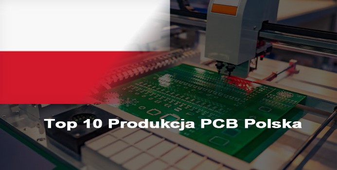
Charger PCBA forms the intelligent, beating heart of every modern power adapter, wireless charging pad, and fast-charging brick. This article delves into the intricacies of charger circuit board assembly, explores key technologies from USB to Qi wireless, and outlines the critical manufacturing controls that guarantee the reliable, high-quality production essential for today’s power devices.
What Production Challenges Exist In Mass Manufacturing Fast / PD Charger PCBA?
- Inconsistent component quality from unreliable suppliers leads to high failure rates.
- Inadequate safety and compliance testing risks product recalls and brand damage.
- Poor thermal management design causes overheating, reducing lifespan and safety.
- Inefficient production scaling results in delays, higher costs, and inability to meet demand.
- Unclear or volatile costing makes budgeting difficult and erodes profit margins.
These hurdles highlight the need for a manufacturing partner with robust systems and deep expertise. A professional charger PCBA factory implements structured solutions to ensure smooth, reliable production.
- Multi-source component procurement & stringent incoming QC to ensure part reliability and supply chain stability.
- Comprehensive, automated testing protocols covering safety, functionality, and regulatory standards.
- Advanced thermal simulation and DFM analysis to optimize PCB layout and component placement.
- Scalable SMT lines and streamlined logistics for high-volume OEM Charger PCBA Manufacturing in China.
- Transparent, detailed quoting based on design complexity, component selection, and volume.
EBest Circuit (Best Technology) is a specialist OEM charger PCBA manufacturer based in China, focused on delivering consistent quality and reliability. We combine engineering expertise with a vertically integrated manufacturing approach, controlling the process from PCB fabrication and component sourcing to assembly and rigorous testing. Our commitment is to be your reliable partner in bringing high-performance, safe, and compliant charging solutions to market. To review your technical requirements in detail, contact our team at sales@bestpcbs.com.
What Is Charger PCBA And How Does It Work In Power Devices?
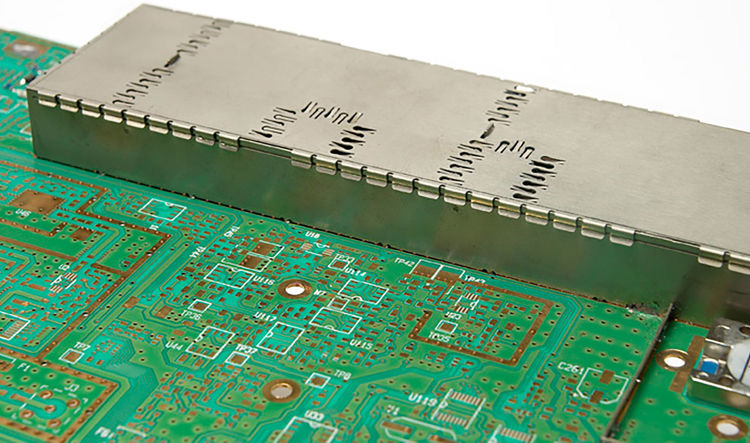
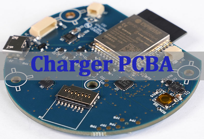
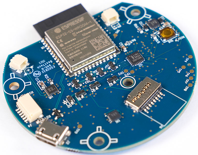
A Charger PCBA (Printed Circuit Board Assembly) is the fully populated circuit board that acts as the control center for any electronic charger. It’s more than just a bare board; it’s the integrated platform where components like ICs, resistors, capacitors, and connectors are soldered to execute the charger’s core function: converting and managing electrical power safely and efficiently for devices.
The core workflow involves several key stages managed by the circuit:
- AC-to-DC Conversion (For Wired Chargers): The input AC power is rectified and stepped down to a lower voltage.
- Power Regulation & Management: A dedicated controller IC (e.g., for USB PD or QC protocols) regulates voltage and current.
- Communication & Handshake: For smart chargers (Fast / PD Charger PCBA), the board communicates with the device to negotiate the optimal voltage/current profile.
- Safety Protection: Circuits monitor for over-voltage, over-current, over-temperature, and short circuits, cutting off power if thresholds are exceeded.
- Stable Output: Finally, it provides a clean, stable DC output through the USB port or induces a current in a Wireless Charger PCBA.
In essence, the Charger PCBA is the engineered bridge between wall power and your sensitive device, ensuring safe, efficient, and rapid energy transfer.
What Makes Wireless Charger PCBA Different From Wired Charger PCBA?
The fundamental difference lies in how power is transferred, which drives two very different PCBA architectures.
Wired charger PCBA relies on direct electrical conduction, while wireless charger PCBA is built around inductive energy coupling and electromagnetic control.
Wired vs Wireless Charger PCBA – Key Differences
| Aspect | Wired Charger PCBA | Wireless Charger PCBA |
|---|---|---|
| Power Transfer | Direct electrical conduction | Inductive coupling |
| Core Interface | Cable and connector | Transmitting (Tx) coil |
| Key Focus | Power efficiency & protocol compliance | Coil tuning & EMI control |
| Communication | USB-based protocols | In-band modulation (Qi) |
| Safety Mechanism | Electrical protection | FOD & thermal monitoring |
| User Interaction | Plug-in connection | Placement and alignment |
Unlike a wired charger PCBA, which prioritizes voltage regulation, protocol negotiation, and thermal dissipation, wireless charger PCBA introduces an additional electromagnetic system layer.
This requires precise coil matching, resonant frequency tuning, and robust foreign object detection (FOD) to ensure both charging efficiency and operational safety—capabilities that are not required in standard USB charger PCBA manufacturing.
Why Is Qi Wireless Charger PCBA Critical For Compatibility And Safety?
The Qi Wireless Charger PCBA is critical because it embodies adherence to the universal Qi standard, which is not just about convenience but a strict framework for interoperability and safety. A non-compliant board can fail to charge, damage devices, or pose physical hazards.
A properly designed Qi PCBA ensures:
- Universal Compatibility: It guarantees operation with any Qi-certified smartphone or device, a key selling point.
- Safe Operation: It integrates mandatory Foreign Object Detection (FOD). The PCBA constantly monitors for metal objects like keys or coins that could overheat, and shuts down power if detected.
- Efficient Power Transfer: The circuit is tuned to the Qi-specified frequency band (typically 110-205 kHz), optimizing energy transfer and minimizing loss.
- Regulatory Compliance: Qi certification involves passing rigorous tests for EMI, thermal performance, and safety, which the PCBA design must inherently support.
- Communication Integrity: It correctly handles the Qi communication protocol, allowing the charger and device to exchange vital data on power needs and status.
Without a PCBA built to the exacting Qi standard, a wireless charger is unreliable, potentially unsafe, and incompatible with the market it intends to serve.
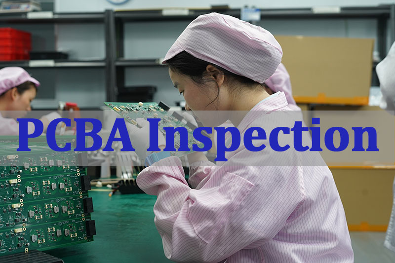
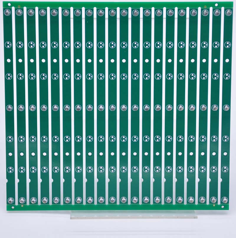
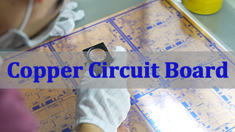
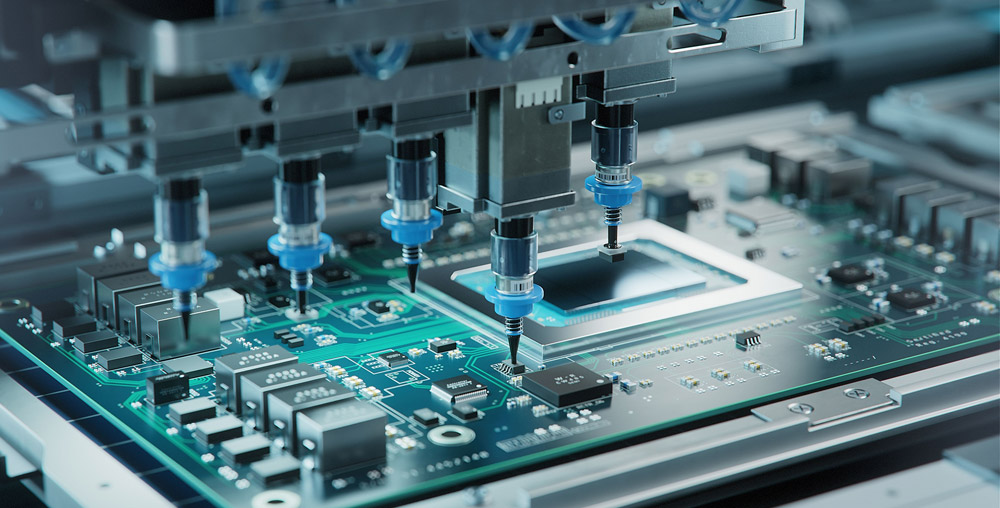
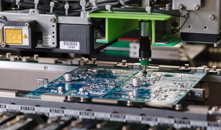
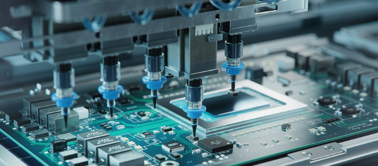
What Manufacturing Controls Ensure Consistent Quality In USB Charger PCBA Production?
Consistent quality in USB Charger PCBA production doesn’t happen by accident; it is the result of a controlled, multi-layered manufacturing process. For an OEM wireless charger PCBA manufacturer, these controls are non-negotiable to ensure every unit performs identically and safely.
Key controls include:
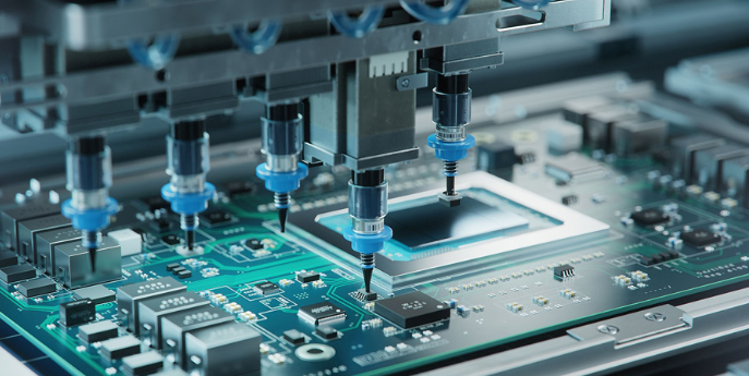
- DFM/DFA Analysis: Design for Manufacturability/Assembly reviews catch potential issues (component spacing, thermal pads) before production begins.
- Automated Optical Inspection (AOI): Post-solder, AOI machines use cameras to detect soldering defects, missing components, or misalignment.
- In-Circuit Testing (ICT): Electrical probes test individual components and circuit connections on the PCB for shorts, opens, and correct values.
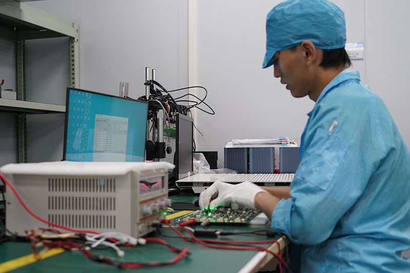
- Functional & Load Testing: Every PCBA is powered and subjected to simulated operational tests, including output voltage/current accuracy under load and protocol handshakes (for PD/QC boards).
- Safety Compliance Testing (Sampling/Audit): Regular rigorous tests—hi-pot (dielectric withstand), over-current, over-temperature—are performed to validate safety design.
- Traceability Systems: Barcodes or serial numbers track each batch’s component sources, production date, and test results for accountability.
These systematic checks at critical stages form a quality net, ensuring that only PCBAs meeting all specifications proceed, delivering the consistency promised by a true charger PCBA manufacturer with consistent quality.
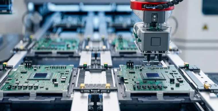
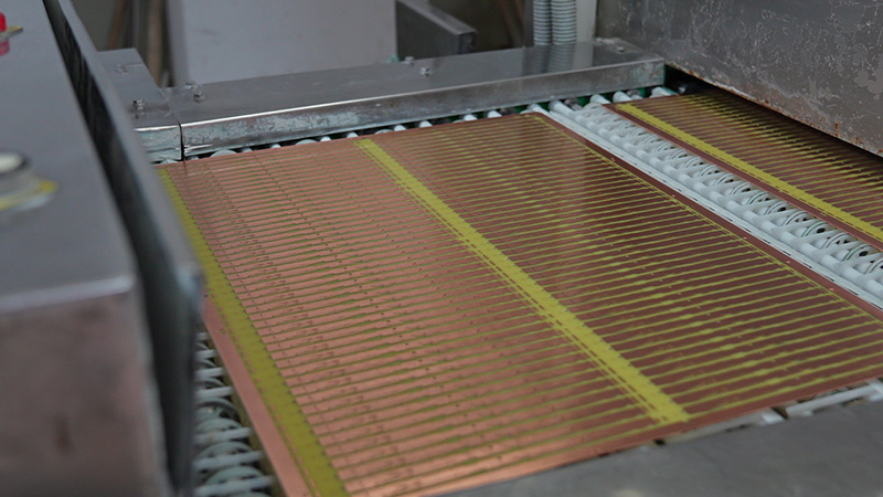
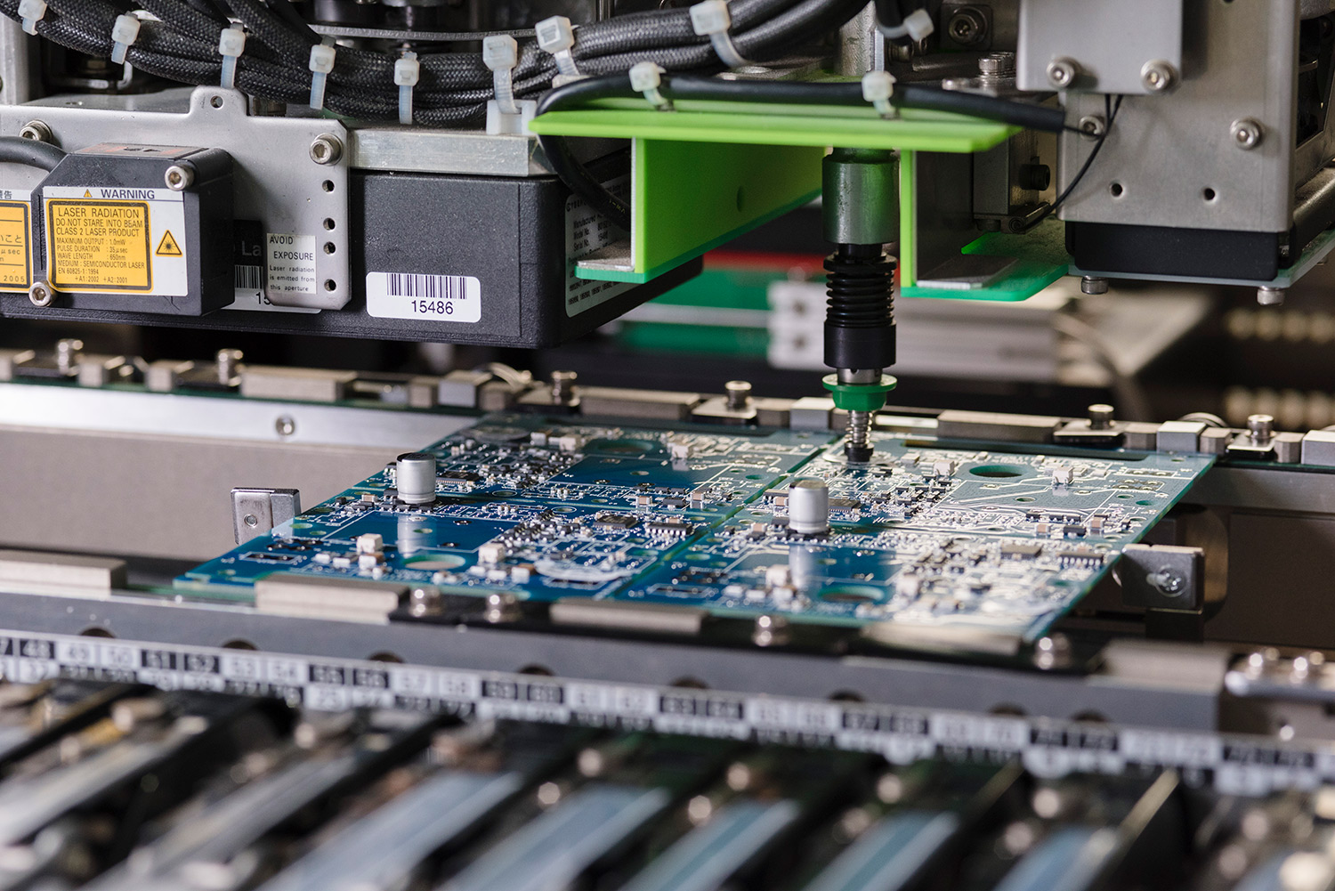
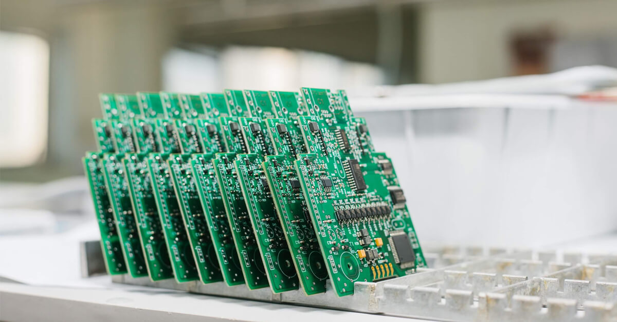
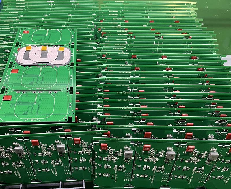
What Capabilities Should A Charger PCBA Factory Provide For Mass Production?
A charger PCBA factory aiming for successful mass production must move beyond basic assembly. It needs integrated capabilities that ensure scalability, quality, and efficiency.
Essential capabilities include:
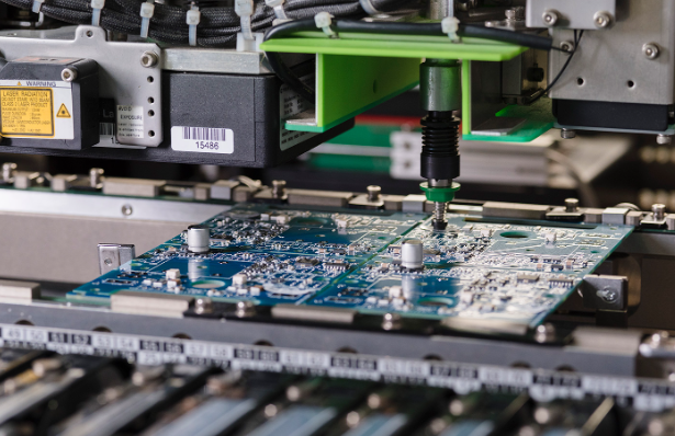
- High-Volume SMT Lines: Automated pick-and-place machines, multi-zone reflow ovens, and conveyor systems for fast, precise assembly.
- Advanced Testing Infrastructure: In-house AOI, ICT, and functional testers for 100% board verification, not just sampling.
- Supply Chain Management: Strong relationships with component distributors and ability to manage long-lead items and buffer stock.
- Engineering Support (NPI): Dedicated New Product Introduction teams to smoothly transition prototypes into mass production.
- Scalable Logistics & Packaging: Efficient warehousing, kitting, and customized packaging solutions for direct shipping.
This combination of technical infrastructure and process expertise allows a factory to reliably turn your OEM Charger PCBA Manufacturing in China project into pallets of finished, tested products ready for the global market.
What Factors Influence Charger PCBA Quotes In OEM Manufacturing Projects?
When requesting charger pcba quotes, it is important to understand that pricing reflects a combination of manufacturing variables rather than a single cost item.
Each factor below directly impacts production efficiency, material usage, and process control requirements.
Key Cost Drivers In Charger PCBA Quotes
| Factor | Cost Impact | Key Consideration |
|---|---|---|
| Order Volume | High | Setup amortization and material scale |
| PCB Complexity | High | Layers, materials, and trace density |
| Component Selection | High | IC type, availability, and sourcing |
| Testing Requirements | Medium | Functional vs. compliance-level testing |
| Assembly Complexity | Medium | Process steps and labor intensity |
Order volume has the strongest influence on unit pricing, as higher quantities spread tooling, setup, and engineering costs across more boards.
PCB complexity and component selection further affect fabrication difficulty and sourcing stability, particularly in power and fast-charging designs.
Testing and assembly requirements determine how much production time, equipment, and manual intervention are required, directly influencing overall manufacturing cost.
A professional charger PCBA manufacturer will clearly break down these factors in the quotation, helping OEM customers balance cost targets with reliability and performance expectations.
Why Choose EBest Circuit (Best Technology) As Your OEM Wireless Charger PCBA Manufacturer In China?
Selecting EBest Circuit (Best Technology) means partnering with a specialist focused on quality, speed, and execution reliability in OEM wireless charger PCBA manufacturing.
Our advantage lies in a well-coordinated, end-to-end manufacturing system designed to support engineering teams from prototype to mass production.
- End-to-End Manufacturing Control: We manage PCB fabrication, component sourcing, SMT assembly, and testing under one integrated manufacturing framework. This minimizes handoff risks, shortens response time, and ensures accountability across every production stage.
- Fast PCBA Turnaround Within 1.5 Weeks: For charger and wireless charger PCBA projects, speed is critical. Our streamlined planning and in-house process control enable PCBA quick-turn delivery in as fast as 1.5 weeks, accelerating validation cycles and reducing time-to-market.
- Quality-First Manufacturing Discipline: We invest in AOI, ICT, and full functional testing to ensure every Qi Wireless Charger PCBA and Fast / PD Charger PCBA meets electrical, thermal, and safety specifications before shipment. Quality is built into the process, not inspected at the end.
- 1 + 3 Engineering Support Model: Each project is supported by one dedicated project engineer plus three specialized technical roles covering DFM review, process engineering, and quality assurance. This structure ensures fast, accurate responses to engineering requirements throughout the full lifecycle.
- Engineering Partnership, Not Just Assembly: We provide actionable DFM feedback to optimize layout, component selection, and thermal design, helping customers achieve stable, cost-effective mass production without repeated redesign.
- Proven Scalability For OEM Programs: Our SMT lines and testing infrastructure are built for volume, supporting consistent quality from pilot builds to millions of units without yield instability or process drift.
- Transparent Communication And Quotation: We provide clear charger PCBA quotes, regular production updates, and dedicated project management, so customers always understand cost structure, production status, and risk control.
All in all, charger PCBA is the critical, engineered core that defines the safety, efficiency, and reliability of modern charging solutions. From understanding the technical nuances of wired versus wireless designs to recognizing the manufacturing controls that ensure quality, selecting the right production partner is the most crucial decision.
For brands seeking a charger PCBA manufacturer with consistent quality, EBest Circuit (Best Technology) offers the technical expertise, rigorous process controls, and scalable production capabilities to bring your projects to market with quick delivery. Pls feel free to contact us anytime for a detailed consultation and quote via sales@bestpcbs.com.
FAQs about Charger PCBA
What Is A PCB Charger?
- A PCB charger is a charger PCBA that handles power conversion, regulation, and protection inside a charging device.
- It is the functional core of USB, fast, and wireless chargers, determining performance, safety, and production consistency.
What Is PCB In Power Electronics?
- In power electronics, a PCB provides the platform for high-current and high-frequency power circuits.
- For charger PCBA manufacturing, PCB design directly impacts efficiency, thermal behavior, and long-term reliability.
Is Qi Wireless Charger PCBA The Same As A Standard Wireless Charger PCBA?
- No. Qi Wireless Charger PCBA is specifically designed to meet the Qi standard, including required communication, safety mechanisms, and system validation for commercial use.
Does PD Charger PCBA Automatically Mean Fast Charging And Mass Production Readiness?
- No. PD Charger PCBA supports the USB Power Delivery open standard, but stable mass production also depends on power topology, thermal design, PCB layout, and SMT process control.
- Unlike QC, which is a private protocol, PD requires consistent hardware execution to ensure reliable charger PCBA manufacturing.