

Wave soldering remains one of the most dependable soldering methods in PCB assembly, especially for through-hole and mixed-technology boards. While surface-mount reflow dominates modern electronics, wave soldering still plays a critical role in industrial control, power electronics, automotive modules, and cost-sensitive high-volume products. Its strength lies in consistency, mechanical robustness, and efficiency when properly controlled.
This guide explains wave soldering from an engineering and manufacturing perspective—how it works, when to use it, how to control defects, and how to select a capable wave soldering partner.
What Is Wave Soldering in PCB Assembly?
Wave soldering is a PCB assembly process where the bottom side of a populated board briefly contacts a controlled wave of molten solder to form solder joints on exposed metal areas, mainly through-hole leads. It is best suited for PCBs with many through-hole components, such as connectors, transformers, relays, and power devices. The process relies on flux activation, controlled preheating, and precise solder contact time to achieve proper wetting and hole fill.
In simple terms, wave soldering uses liquid solder instead of solder paste. This allows many joints to be formed at once, making it efficient and mechanically robust. However, because the entire board bottom passes over molten solder, the process requires careful design rules and parameter control.
Wave soldering is commonly used in industrial control boards, power supplies, automotive modules, and infrastructure electronics, where solder joint strength and consistency are more important than ultra-high component density.
How Does the Wave Soldering Process Work Step by Step?
The wave soldering process consists of four tightly linked stages: flux application, preheating, solder wave contact, and controlled cooling. If defects appear, the root cause almost always traces back to one of these stages being outside its proper process window.
1. Flux Application
Flux is applied to the PCB bottom side by spray or jet. Its job is to remove oxides and promote solder wetting.
- Too little flux → poor wetting, insufficient hole fill
- Too much flux → bridging, residues, solder balls
2. Preheating
Preheating gradually raises the PCB temperature. This activates the flux and reduces thermal shock when the board touches molten solder. Insufficient preheat is one of the most common causes of wave soldering defects.
3. Solder Wave Contact
The PCB passes over one or two solder waves:
- A turbulent wave helps solder penetrate plated through-holes
- A laminar wave smooths the solder fillets
Contact time is controlled by conveyor speed.
4. Cooling
Controlled cooling solidifies the solder joints and stabilizes intermetallic formation. Cooling that is too fast or uneven can affect long-term reliability.
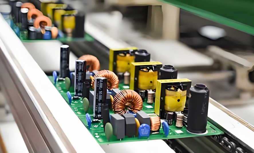
What Types of PCBs Are Best Suited for Wave Soldering?
Wave soldering works best for PCBs with a high proportion of through-hole components and limited bottom-side fine-pitch SMDs. It is especially suitable when mechanical strength and current-carrying capability are priorities.
Typical suitable boards include:
- Power supply PCBs
- Industrial control boards
- Automotive connector boards
- Motor drivers and inverter boards
- Mixed-technology boards with bottom-side protection
Boards that are densely populated with fine-pitch SMDs on the bottom side are usually poor candidates unless pallets or masking are used. From an engineering standpoint, the decision should be made during PCB layout, not after fabrication.
What Are the Key Parameters in Wave Soldering?
Wave soldering quality depends on controlling a group of interacting parameters, not a single setting. Changing one parameter without adjusting others often moves defects rather than eliminating them.
Key parameters include:
- Solder temperature (typically 245–260 °C for lead-free)
- Top-side preheat temperature (commonly 90–130 °C)
- Conveyor speed (controls solder contact time)
- Wave height and angle
- Flux type and application density
A practical rule for beginners:
First stabilize preheat and conveyor speed, then fine-tune flux and wave height.
What Is the Difference Between Wave Soldering and Reflow Soldering?
Wave soldering and reflow soldering serve different assembly needs and should not be treated as interchangeable processes.
Wave Soldering vs Reflow Soldering
| Aspect | Wave Soldering | Reflow Soldering | Engineering Guidance |
|---|---|---|---|
| Main application | Through-hole components | Surface-mount components | Choose based on component type |
| Solder form | Molten solder wave | Solder paste + heat | Fundamentally different |
| Joint strength | Very strong for THT | Optimized for SMD | Power and connectors favor wave |
| Process control focus | Flux, preheat, speed | Paste printing, thermal profile | Different failure modes |
| Typical defects | Bridging, icicles | Tombstoning, voids | Diagnosis differs |
| Cost efficiency | High for THT volume | High for dense SMD | Many products use both |
When Should You Choose Wave Soldering Instead of Selective Soldering?
Wave soldering is preferred when many through-hole joints can be soldered simultaneously without risking bottom-side SMD damage. Selective soldering is better when only a few through-hole components exist.
Wave Soldering vs Selective Soldering
| Factor | Wave Soldering | Selective Soldering | Selection Logic |
|---|---|---|---|
| Through-hole quantity | High | Low | Many joints → wave |
| Flexibility | Lower | Higher | Complex layouts → selective |
| Throughput | High | Medium | Volume favors wave |
| Tooling | Pallets may be needed | Minimal | Depends on layout |
| Cost per board | Lower at scale | Higher | Volume sensitive |
What Are the Advantages of Wave Soldering?
Wave soldering offers high efficiency, strong solder joints, and excellent through-hole fill when properly controlled. These advantages explain why it remains common in power and industrial electronics.
- High throughput for THT assemblies
- Strong mechanical solder joints
- Reliable hole fill on thick boards
- Lower unit cost at medium to high volume
- Proven long-term reliability
For applications exposed to vibration, current load, or thermal cycling, wave soldering remains a solid engineering choice.
What Are the Limitations of Wave Soldering?
The main limitation of wave soldering is its lack of selectivity. Because the entire board bottom contacts molten solder, fine-pitch bottom-side SMDs require protection.
- Higher bridging risk on dense layouts
- Need for pallets or masking in mixed assemblies
- Less flexibility than selective soldering
- Greater sensitivity to PCB layout rules
These limitations reinforce the importance of early DFM review.
What Are Common Wave Soldering Defects and Their Causes?
Most wave soldering defects result from imbalance between flux activity, preheating, and solder contact time. Understanding the cause-and-effect relationship is critical.
Common Defects, Causes, and Fixes
| Defect | Appearance | Root Cause | Primary Correction |
|---|---|---|---|
| Bridging | Adjacent joints connected | Excess solder, slow speed | Reduce wave height, increase speed |
| Icicles | Sharp solder spikes | Poor drainage | Adjust exit angle, improve preheat |
| Poor hole fill | Incomplete solder rise | Low preheat, weak flux | Increase preheat, adjust flux |
| Non-wetting | Dull or missing solder | Oxidation, contamination | Improve cleaning, flux activity |
How Can You Reduce Wave Soldering Defects?
Defect reduction starts at PCB design and is locked in during first-article setup. Most defects cannot be “fixed” later without redesign or process instability.
- Proper pad spacing and solder mask design
- Use of solder thieves where necessary
- Matching flux chemistry to PCB finish
- Stable preheat and conveyor speed
- First-article verification and SPC monitoring
From experience, investing time in setup saves far more time in rework.
How Much Does Wave Soldering Cost in PCB Assembly?
Wave soldering cost depends on board size, through-hole count, production volume, and tooling needs—not just the process itself.
Cost Structure Overview
| Cost Element | What Drives It | How to Optimize |
|---|---|---|
| Equipment & line time | Throughput, utilization | Efficient scheduling |
| Solder & flux | Alloy, consumption control | Proper maintenance |
| Tooling | Pallets, masking | DFM optimization |
| Labor & inspection | Yield, rework rate | Stable process |
| Defects & scrap | Process variation | Early validation |
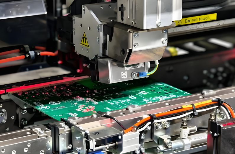
Why Choose EBest as Your Wave Soldering Manufacturer?
When selecting a wave soldering partner, the most important factor is process discipline, not equipment alone. An experienced manufacturer understands how layout, materials, and parameters interact.
Best Technology provides wave soldering services with strong engineering support, including:
- Dedicated wave and selective soldering lines
- Nitrogen-assisted wave soldering capability
- DFM feedback focused on defect prevention
- Experience with industrial, automotive, and power electronics
- Integrated PCB fabrication and PCBA production
This reduces risk and improves consistency from prototype to mass production.
EBest Circuit Wave Soldering Capabilities
| Item | EBest Capability Data |
| Soldering Process | Lead-free wave soldering |
| Supported Alloys | SAC305 / SAC405 |
| Solder Pot Temp. | 245–260 °C |
| Temp. Stability | ±2 °C |
| Conveyor Speed | 0.8–1.8 m/min |
| Speed Resolution | Fine adjustable |
| Preheat Zones | Multi-zone |
| Top-Side Preheat | 90–130 °C |
| Preheat Uniformity | Controlled |
| Wave Type | Dual wave |
| Turbulent Wave | Supported |
| Laminar Wave | Supported |
| Wave Height | Adjustable |
| Contact Time | Speed-controlled |
| Nitrogen Mode | Supported |
| O₂ Level (N₂) | Low-oxygen environment |
| Flux Type | No-clean / Water-soluble |
| Flux Method | Spray |
| Flux Volume | Adjustable |
| PCB Thickness (Min) | ~0.8 mm |
| PCB Thickness (Max) | ~3.2 mm |
| Copper Weight | Std / Heavy copper |
| Through-Hole Density | High pin-count |
| Lead Diameter | Thick leads supported |
| Hole Aspect Ratio | High AR supported |
| Hole Fill | High consistency |
| Bottom-Side SMD | Pallet / masking |
| Pallet Support | Custom pallets |
| PCB Surface Finish | HASL / ENIG / ENEPIG |
| Solder Mask | LPI |
| Board Size | Conveyor adjustable |
| First Article | Mandatory |
| Parameter Lock | After FA approval |
| Process Monitoring | In-line |
| Defect Focus | Bridging / Icicles / Hole fill |
| Rework | Manual / Selective |
| Production Volume | Prototype → Mass |
| Typical Applications | Power / Industrial / Automotive / Medical / Aerospace / Military |
FAQ — Common Questions About Wave Soldering
1. What is wave soldering used for in PCB assembly?
Wave soldering is mainly used for through-hole components that require strong mechanical joints, such as connectors and power devices.
2. What temperature is used for lead-free wave soldering?
Most lead-free wave soldering processes operate between 245 °C and 260 °C, depending on alloy and board design.
3. How do you prevent bridging in wave soldering?
Bridging is reduced by optimizing wave height, increasing conveyor speed, improving solder mask design, and controlling flux volume.
4. How can you improve through-hole fill in wave soldering?
Adequate preheating, active flux, and sufficient solder contact time are the most effective ways to improve hole fill.
5. What PCB thickness works best for wave soldering?
Most boards from 1.0 mm to 3.2 mm are suitable with proper preheat control.
6. Is wave soldering better than selective soldering for THT boards?
For boards with many through-hole joints, wave soldering is usually faster and more cost-effective.
7. Can wave soldering be used for mixed THT and SMD boards?
Yes, but bottom-side SMDs must be protected using pallets, masking, or adhesive methods.