

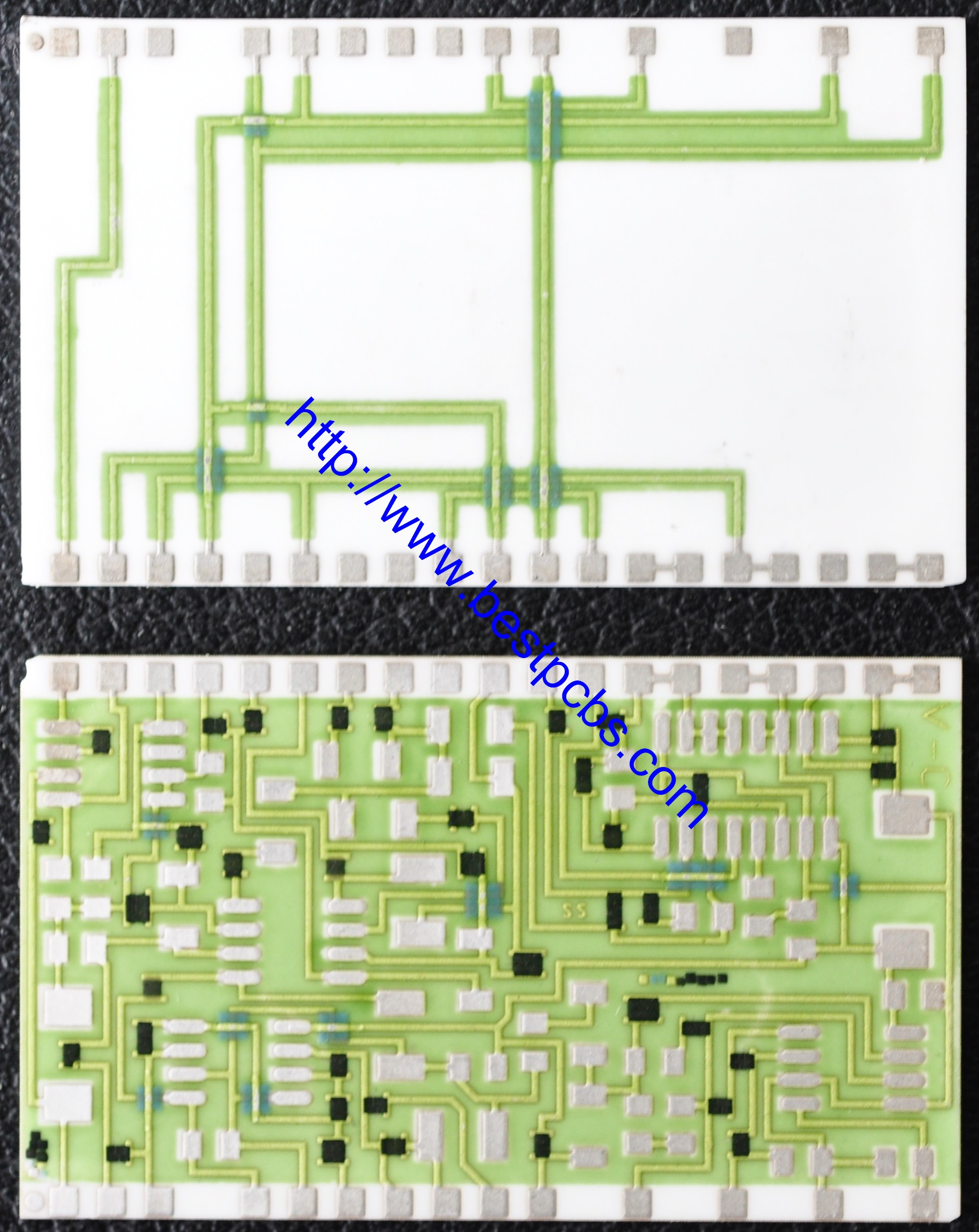
What Is a Thick Film Ceramic PCB?
A thick film ceramic PCB is made by screen-printing functional pastes onto a ceramic base and then sintering the printed layers at high temperature. After firing, the material forms durable conductive paths or functional structures on the ceramic surface. In simple terms, a thick film ceramic circuit board combines the stability of a ceramic base with printed electrical features that can support conductors, resistors, and other functional layers.
The term “thick film” refers to the thickness of the printed conductive or resistive layer. In most cases, the conductor thickness starts at around 10 μm and often falls in the 10 to 13 μm range, with some designs reaching 20 μm. This is thicker than the metallization used in thin-film ceramic technology, but still thinner than the copper structure commonly found in DCB ceramic boards or standard FR4 boards.
A thick film ceramic substrate can do more than carry conductor traces. It can also support:
- Conductors
- Printed resistors
- Dielectric layers
- Cross-over conductors
- Semiconductor-related functional structures
Because of this flexibility, thick film ceramic PCB is widely used in hybrid modules, sensor circuits, and compact control electronics.
Thick Film vs Thin Film Ceramic PCB
The comparison between thick film vs thin film ceramic PCB is one of the most common questions in ceramic electronics. Although both technologies use ceramic materials as the base, their process routes, cost structures, and application focus are quite different.
| Item | Thick Film Ceramic PCB | Thin Film Ceramic PCB |
| Main Process | Screen printing + firing | Vacuum deposition or sputtering |
| Typical Conductor Thickness | 10–20 μm | Much thinner |
| Cost Position | More economical for many industrial uses | Usually higher |
| Printed Resistor Integration | Easy | Less common |
| Fine-Line Capability | Moderate | Higher |
| Typical Use | Hybrid circuits, sensors, power-related modules | Precision circuits and ultra-fine patterns |
In practical use, thick film ceramic PCB is often selected when the design needs better functional integration, a stable ceramic base, and a more workable cost. Thin film ceramic PCB is more suitable when very fine line resolution or higher pattern precision is the priority.
What Materials Are Used in an Alumina Ceramic Thick Film PCB?
An alumina ceramic thick film PCB is the most common version of this technology. The substrate is usually made from 96% or 98% alumina, because alumina offers a strong balance of electrical insulation, thermal resistance, and manufacturing practicality. For applications that require higher thermal conductivity, AlN is also a common choice. In some specialized cases, beryllium oxide may be used as well.
Common Substrate Materials
| Material | Typical Feature | Notes |
| 96% Alumina | Standard industrial choice | Good balance of cost, insulation, and manufacturability |
| 98% Alumina | Higher purity | Better stability for more demanding designs |
| AlN | High thermal conductivity | Often used in high-power modules and applications with strict heat dissipation needs |
| BeO | Excellent thermal conductivity | Used in specialized applications with stricter handling and safety requirements |
Common Substrate Thickness Options
- 0.25 mm
- 0.38 mm
- 0.50 mm
- 0.635 mm
- 0.76 mm
- 1.0 mm
- 1.6 mm or 2.0 mm as custom options
Common Conductor Materials
| Conductor Material | Typical Use |
| Silver-Palladium | Common and more cost-effective |
| Gold-Palladium | Premium applications and bonding-friendly designs |
| Mo/Mn + Ni | Certain special environments, including ozone-related use |
The choice of thick film ceramic substrate material affects both cost and performance. For example, gold-palladium is far more expensive than silver-palladium, so it is generally used only when the application truly needs its bonding or performance advantages.
What Are the Main Technical Parameters in Thick Film PCB Manufacturing?
When evaluating thick film PCB manufacturing capability, engineers usually focus on conductor thickness, minimum line width, resistor integration, and possible layer count. These factors directly affect whether the board can match the intended circuit design.
| Parameter | Typical Capability |
| Substrate Material | 96% / 98% Alumina, AlN, BeO |
| Conductor Thickness | ≥10 μm, up to 20 μm |
| Standard Trace/Space | 0.30 / 0.30 mm |
| Finer Production Capability | 0.20 / 0.20 mm with higher cost |
| Prototype Fine Line | 0.15 / 0.20 mm in limited cases |
| Final Trace Layout Tolerance | ±10% |
| Typical Layers | 1L and 2L |
| Maximum Layers | Up to 10L |
| PTH | Available for selected multilayer or double-sided designs |
| Solder Mask | Optional |
| Solder Mask Color | Semi-transparent |
| Solder Mask Heat Resistance | Above 500°C |
These parameters show why thick film PCB manufacturing is well suited to many industrial, automotive, lighting, and sensor-related designs. It is not aimed at ultra-fine microelectronic geometry, but it offers very good process stability for a broad range of practical applications.
Can a Thick Film Printed Resistor Ceramic Board Integrate Different Resistor Values?
Yes. One of the strongest advantages of a thick film printed resistor ceramic board is that resistor elements can be integrated directly onto the ceramic surface. This means one substrate can carry conductors and resistors together, reducing the need for extra discrete components in some designs.
A thick film printed resistor ceramic board can include:
- A single resistor value across the entire design
- Different resistor values in different circuit areas
- Combined conductor and resistor functions on one substrate
That is why thick film ceramic PCB is often used in resistor cards, hybrid circuits, analog control modules, and sensor products. At the same time, resistor complexity affects cost. In general, the more resistor values placed on one board, the more difficult the process becomes, and the higher the price is likely to be.
Can Thick Film Ceramic PCB Support Wire Bonding?
Yes, thick film ceramic PCB can support wire bonding, but the requirement should be defined early. Both gold-palladium and selected silver-palladium conductor systems can support gold wire bonding, although not every standard conductor paste is equally suitable for that purpose.
If wire bonding is required, the supplier should know this during quotation and engineering review. That early confirmation helps with:
- Correct conductor system selection
- Better process compatibility
- Improved bonding reliability in production
For bonding-related projects, early material matching is always more effective than changing the design later.
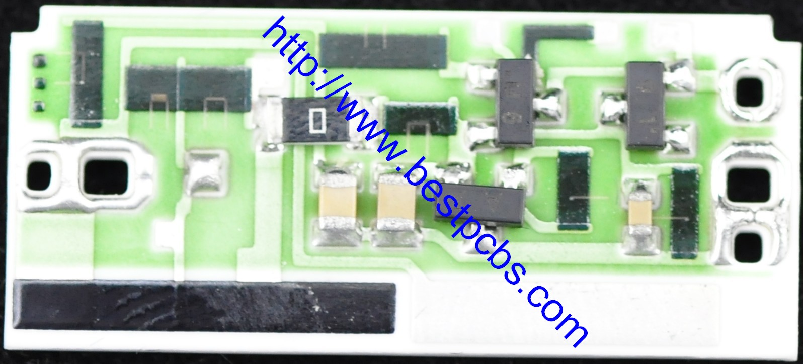
What Board Structures Are Available for a Thick Film Hybrid Circuit Board?
A thick film hybrid circuit board is most commonly produced as a 1-layer or 2-layer design, but multilayer structures are also possible for more complex projects. Because a ceramic thick film circuit can integrate conductors and resistor functions on the same substrate, it is often chosen for compact modules that need both electrical function and dimensional stability.
Common Build Styles
- Single-sided thick film hybrid circuit board
- Double-sided thick film ceramic PCB
- Multilayer ceramic thick film circuit structures
- PTH-supported designs for selected projects
- Optional solder mask upon request
Shape and Delivery Notes
- Rectangular boards are the most common format
- Boards can be shipped as single pieces
- Boards can also be delivered in panel form
For standard production, rectangular shapes are usually the easiest to process, inspect, and ship. In most cases, they also provide the best balance between manufacturing efficiency and handling convenience.
What Are the Most Common Thick Film Ceramic PCB Applications?
Thick film ceramic PCB applications are broad, especially in products that need heat resistance, electrical stability, and compact function integration. Because the ceramic base can remain stable under demanding conditions, this technology is widely used across industrial and automotive sectors.
Typical Applications
- High-power LED
- Street light
- High-brightness lighting
- Automotive light systems
- Hybrid integrated circuits for automotive
- Fuel sender resistor card
- Injection systems
- Anti-lock braking systems
- High-power semiconductor modules
- Electric power transmitter modules
- Semiconductor process equipment
- Solar cell applications
- Sensors
- Telecommunication devices
- Chip and wafer-related electronic applications
What Affects the Cost of Thick Film Ceramic PCB?
The cost of thick film ceramic PCB depends on material selection, conductor system, resistor design, and processing difficulty. Even when two projects look similar on the surface, their price can change noticeably if the conductor material, resistor count, or line definition is different.
Main Cost Factors
- Gold-palladium is much more expensive than silver-palladium
- More resistor values on the same board increase cost
- Finer trace and spacing increase process difficulty
- More layers add complexity
- Special substrate thickness adds cost
- Bonding-compatible conductor systems may require special materials
- Small prototype runs with fine features often cost more per piece
For many engineers, thick film ceramic PCB offers a useful performance upgrade over standard boards without reaching the cost level of DCB in many practical use cases.
What Should Buyers Confirm Before Ordering?
A clear design review before production helps avoid rework, shorten communication time, and improve quotation accuracy. This is especially important for ceramic projects, where material and conductor choices directly affect the process route.
Buyer Checklist
- Substrate material
- Ceramic purity
- Substrate thickness
- Conductor material
- Conductor thickness requirement
- Minimum trace and spacing
- Number of resistor values
- Whether wire bonding is required
- Whether PTH is needed
- Layer count
- Solder mask requirement
- Single-piece or panel delivery
If you are interested in thick film ceramic PCB, please contact us today for more information about Thick Film Ceramic circuit board.