

RF antenna PCB technology has become a fundamental component in modern wireless electronics. From IoT modules and smart devices to automotive radar and satellite communication systems, engineers increasingly rely on PCB-integrated antennas to reduce system size, improve signal efficiency, and simplify hardware integration.
However, designing and manufacturing RF antenna PCBs presents unique engineering challenges. Common engineering challenges include:
- Signal loss at GHz frequencies
- Impedance mismatch causing reflection
- Antenna tuning instability
- Limited board space for antenna structures
- Inconsistent RF performance during production
Matching Solutions
- Controlled impedance stack-up design
- RF simulation during PCB layout
- Dedicated antenna tuning zones
- Low-loss RF laminate materials
- Precision manufacturing processes
EBest Circuit (Best Technology) is an engineering-driven PCB and PCBA manufacturer with extensive experience in RF PCB fabrication and antenna integration. Our engineering team collaborates closely with product designers to optimize antenna layout, impedance control, and RF signal routing before production begins.
We support prototype, small-volume production, and scalable manufacturing for wireless communication devices. With in-house PCB fabrication and assembly capability, we ensure consistent RF performance from design verification to mass production. Our engineers assist with RF stack-up design, impedance simulation, and antenna performance optimization to reduce development risks and shorten product launch cycles. For RF antenna PCB manufacturing support, pls feel free to contact us at sales@bestpcbs.com.
What Is RF Antenna PCB And Why Is It Critical In Modern Wireless Systems?
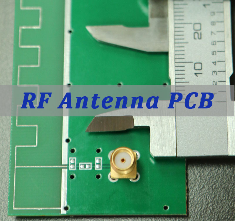
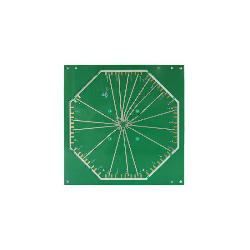
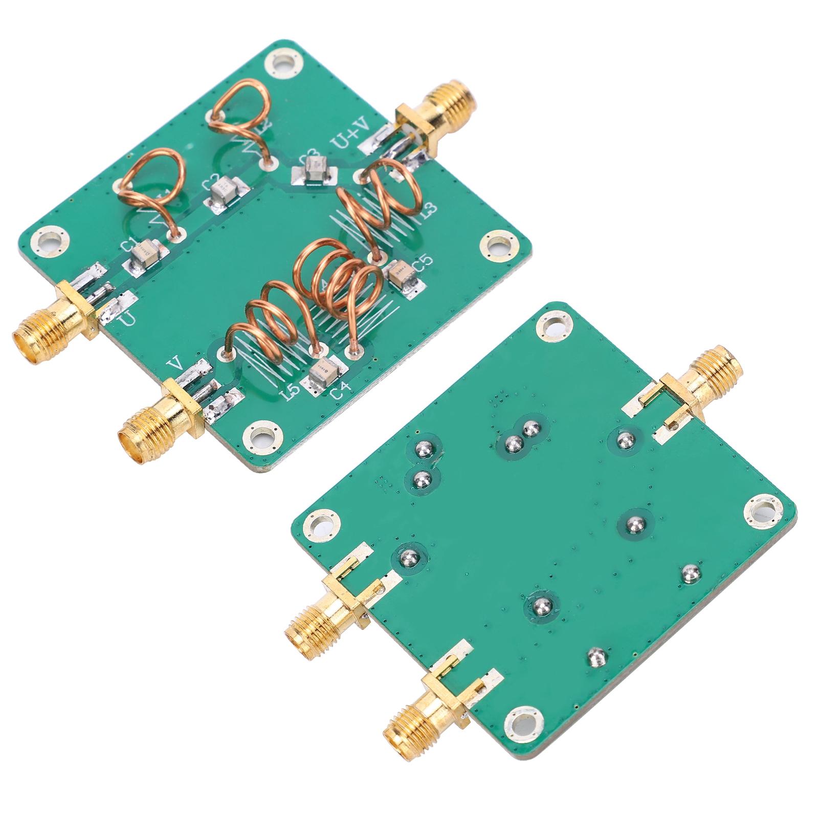
An RF antenna PCB integrates the antenna structure directly onto a printed circuit board rather than using external antenna components. This allows wireless devices to achieve compact design, reduced assembly complexity, and improved electromagnetic compatibility.
RF antenna PCBs operate at high frequencies such as 2.4 GHz, 5 GHz, or even millimeter-wave bands. At these frequencies, even small variations in trace geometry or dielectric properties can significantly affect signal performance.
Typical RF antenna PCB applications include:
- IoT communication modules
- Bluetooth devices
- WiFi routers and gateways
- automotive radar sensors
- wireless medical equipment
From an engineering perspective, integrating the antenna onto the PCB reduces connector losses and ensures better system integration. With this in mind, understanding how PCB antennas actually function helps engineers design more efficient RF circuits.
How Does A PCB RF Antenna Work In Wireless Communication Circuits?
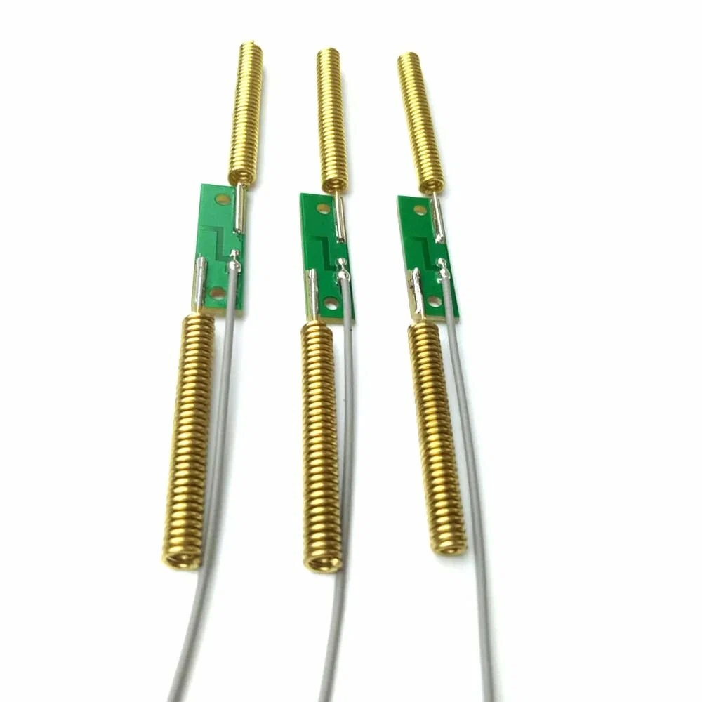
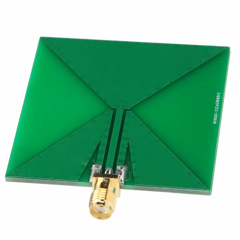
A PCB RF antenna converts electrical RF signals into electromagnetic waves that propagate through space. The antenna geometry determines radiation pattern, gain, and frequency bandwidth.
Common PCB antenna structures include:
| Antenna Type | Typical Application |
|---|---|
| Inverted-F antenna (IFA) | Smartphones and IoT |
| Meander antenna | Compact wearable devices |
| Patch antenna | GPS and satellite systems |
| Monopole antenna | Wireless modules |
These antennas rely on carefully tuned trace lengths and ground reference planes to achieve resonance at target frequencies.
Design considerations include:
- Trace length relative to wavelength
- Ground plane size
- dielectric constant of PCB material
- impedance matching networks
Under real manufacturing conditions, small geometry changes may affect antenna resonance frequency. As a result, understanding antenna structure differences becomes critical for RF PCB design.
What Are The Key Differences Between RF PCB Antenna And Traditional Antennas?
An RF PCB antenna differs from traditional metal antennas because it is fabricated directly on the PCB copper layer. This integration significantly reduces system complexity.
Key comparison:
| Feature | PCB Antenna | Traditional Antenna |
|---|---|---|
| Integration | Built into PCB | External component |
| Size | Compact | Larger |
| Assembly | Simplified | Requires connectors |
| Cost | Lower in mass production | Higher |
However, PCB antennas require precise design and simulation to ensure correct radiation performance.
Engineers must also consider:
- substrate dielectric constant
- copper thickness
- antenna clearance area
- ground isolation
In practice, antenna performance depends heavily on PCB layout decisions. That said, antenna design on PCB requires specialized RF design methodologies.
Why Do Engineers Focus On RF Antenna Design On PCB During Product Development?
RF antenna design on PCB directly determines wireless performance and signal reliability. Poor antenna design may lead to low transmission range or unstable connectivity.
Key engineering objectives include:
- Achieving correct resonance frequency
- Maintaining impedance matching (50Ω)
- Optimizing radiation efficiency
- Minimizing signal reflection
Design engineers typically perform:
- electromagnetic simulation
- antenna tuning
- impedance matching network design
- prototype validation testing
These steps ensure the antenna performs consistently in the final product environment. From an engineering perspective, the next step is understanding the detailed design factors influencing RF antenna performance.
What Are The Most Important Factors In RF PCB Antenna Design?
RF PCB antenna design requires careful attention to both electrical and physical design parameters.
Important design variables include:
PCB Material
- FR4 for cost-sensitive designs
- Rogers materials for high-frequency performance
Trace Geometry
- Antenna length must match resonance frequency
- Smooth trace edges reduce signal loss
Ground Clearance
- Adequate spacing prevents signal interference
Matching Network
- Used to optimize antenna impedance
Engineering simulations often validate these parameters before prototype production. More importantly, stable manufacturing processes are required to maintain these design parameters during production.
Why Choose A PCB RF Antenna Manufacturer For Stable Production?
A professional pcb rf antenna manufacturer ensures that RF design parameters remain consistent across production batches.
Key manufacturing capabilities include:
- controlled impedance fabrication
- high-precision PCB etching
- RF laminate processing
- impedance testing and verification
Manufacturers also monitor critical variables:
| Parameter | Importance |
|---|---|
| dielectric thickness | controls impedance |
| copper thickness | affects RF loss |
| trace accuracy | ensures antenna resonance |
Under real manufacturing conditions, these parameters must remain tightly controlled. In contrast, supplier capability becomes equally important when scaling production volumes.
What Should You Expect From A PCB RF Antenna Supplier For Industrial Projects?
A reliable pcb rf antenna supplier provides more than fabrication services. Engineering collaboration is essential for successful RF product development.
Typical supplier capabilities include:
- DFM analysis for RF circuits
- impedance stack-up design
- antenna layout optimization
- prototype validation
A good RF PCB supplier should also provide:
- RF material sourcing
- quick prototype turnaround
- stable production quality
Ultimately, engineering support reduces product development risk and improves wireless performance. Ultimately, many companies evaluate global manufacturing options for RF PCB production.
Why Are Many OEMs Working With A China PCB RF Antenna Manufacturer?
A china pcb rf antenna manufacturer offers competitive advantages in both engineering capability and manufacturing scalability.
Many OEMs choose Chinese manufacturers for:
- advanced PCB fabrication equipment
- competitive production costs
- experienced RF manufacturing teams
- flexible prototype services
China’s PCB industry also benefits from mature supply chains for:
- RF laminate materials
- precision PCB fabrication
- high-volume assembly services
These factors allow companies to accelerate product development cycles while controlling production costs. All things considered, choosing the right manufacturing partner ultimately determines RF PCB project success.
How Can EBest Deliver Reliable RF Antenna PCB Manufacturing Services?
EBest Circuit provides specialized rf antenna pcb manufacturing for wireless communication applications. Our engineering team supports RF design optimization, prototype validation, and stable production.
Key advantages include:
- integrated PCB fabrication and assembly
- RF material processing capability
- engineering-led manufacturing support
- strict quality control systems
Our engineers collaborate with customers to refine antenna layout and impedance matching before production begins. This approach improves signal reliability and reduces product development risk.
In summary, RF antenna PCB manufacturing requires close cooperation between design engineers and experienced PCB manufacturers.
To summarize, rf antenna pcb design and manufacturing play a critical role in modern wireless communication devices.
Careful antenna layout, impedance control, and RF material selection ensure stable signal performance.
Working with an experienced RF PCB manufacturer reduces development risks and improves production reliability.
For RF antenna PCB manufacturing support, contact sales@bestpcbs.com.
FAQs About RF Antenna PCB
What frequency ranges are commonly used for RF antenna PCB designs?
Most RF antenna PCBs operate at 2.4 GHz, 5 GHz, 900 MHz, and sub-GHz bands depending on application requirements such as WiFi, Bluetooth, or IoT connectivity.
Which PCB materials are best for RF antenna PCB manufacturing?
FR4 can be used for low-cost designs, but Rogers, Taconic, or PTFE materials provide better performance for high-frequency RF circuits.
How is RF antenna performance tested on a PCB?
Engineers typically use vector network analyzers (VNA) to measure impedance matching, return loss, and antenna efficiency.
Can RF antenna PCBs be produced in small batches?
Yes. Many manufacturers support RF PCB prototyping and small-volume production, allowing engineers to validate antenna designs before mass production.