PCB manufacturing PCB manufacturing
Home > Blog

Posts Tagged ‘microwave pcb material’

What Does DK Mean in RF PCB Material? How to Choose it?
Wednesday, December 10th, 2025

In RF and microwave PCB materials, DK means Dielectric Constant, also known as relative permittivity (εr).

Designing an RF or microwave PCB involves far more than routing traces—you must understand how materials behave at high frequencies. One of the most critical parameters is DK. Whether you are building a 1 GHz RF amplifier, a 10 GHz radar board, or a 77 GHz millimeter-wave automotive sensor, DK directly affects signal integrity, impedance, and loss.

This guide covers what DK means, why it matters, how it affects impedance, common RF PCB materials and their DK values, and how to choose the right laminate for RF, microwave, and mmWave designs.

What Does DK Mean in RF PCB Material? How to Choose it?

What Does DK Mean in RF PCB Material?

DK = Dielectric Constant = Relative Permittivity (εr)

It describes how much an RF signal slows down as it passes through the PCB substrate.

  • Air has DK ≈ 1
  • FR-4 has DK ≈ 4.2–4.8
  • RF materials like Rogers typically have DK ≈ 2.2–3.5

In RF engineering, DK affects:

  • signal speed
  • impedance
  • wavelength
  • phase stability
  • overall RF performance

Lower DK materials allow signals to travel faster and lose less energy, which is why they are widely used in RF, microwave, 5G, and mmWave designs.

Importance of DK in Impedance Control

Controlled impedance is required for RF transmission lines such as microstrip, stripline, and CPW structures.

DK directly affects characteristic impedance (Z₀), because:

Importance of DK in Impedance Control

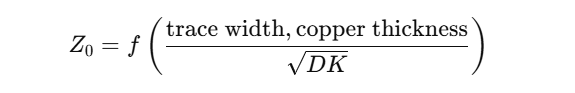
If the DK varies, impedance varies—and this creates reflection, mismatch, and signal loss.

This means:

  • If DK increases → impedance decreases
  • If DK decreases → impedance increases

Consistency is everything. Even a 1–2% DK variation can shift the impedance by noticeable amounts, leading to:

  • signal reflections
  • poor return loss
  • increased insertion loss
  • degraded power transfer

Therefore, RF PCB materials must have tight DK tolerance, usually around ±0.04 or better.

How Does DK Affect Impedance Control in RF PCBs?

Understanding DK helps engineers design stable, predictable transmission lines.

1. Impedance Matching

Lower DK requires wider traces to maintain 50Ω impedance. Higher DK requires narrower traces, which increases fabrication difficulty.

2. Phase Velocity & Delay

Signal speed is inversely related to DK:

How Does DK Affect Impedance Control in RF PCBs?

Lower DK → faster signal → better phase performance.

This matters in:

  • phased-array antennas
  • differential pair timing
  • radar systems
  • power dividers & couplers

3. Dielectric Loss

While DF (dissipation factor) is the main loss-related parameter, DK influences how the electromagnetic field interacts with the substrate.

Higher DK = more energy trapped in substrate = higher loss at microwave frequencies.

4. Manufacturing Tolerances

Low DK materials allow wider traces, which reduces:

  • etching variation
  • copper width tolerance
  • impedance deviation between batches

This makes low-DK materials more manufacturable for high-volume RF boards.

Common Types of RF PCB Materials

Below are the most widely used material categories for RF, microwave, and mmWave PCBs.

1. FR-4 (Limited RF Use)

  • DK = 4.2–4.8
  • Usable for ≤ 1 GHz
  • High loss, unstable DK, poor high-frequency performance

Not suitable for microwave or 5G boards.

2. Hydrocarbon Ceramic Laminates (Rogers RO4000 Series)

Examples: RO4003C, RO4350B, RO4835

  • DK ≈ 3.27–3.48
  • Low loss
  • Stable DK across frequency
  • Compatible with FR-4 manufacturing

Ideal for: WiFi antennas, RF amplifiers, 10–20 GHz radar, high-power RF designs.

3. PTFE-Based RF Materials

Examples: RT/duroid 5880, RT/duroid 6002, RO3000 series

  • DK = 2.17–3.0
  • Very low loss
  • Best for 24–80 GHz mmWave
  • Requires specialized processing

Used in: ADAS 77 GHz radar, satellite RF modules, high-end filters, mmWave front-end designs.

4. Ceramic-Filled PTFE & Hybrid Laminates

Used in ultra-high-frequency and high-reliability applications:

  • stable DK
  • low CTE
  • excellent thermal stability

Applications: Space, military RF systems, phased-array radar.

Here is a summarized RF material parameter:

Material CategoryTypical DKFrequency UseNotes
FR-44.2–4.8<1 GHzHigh loss, unsuitable for RF/microwave
Rogers RO4000 Series3.27–3.551–20 GHzCost-effective, stable DK
Rogers RO3000 Series3.0, 3.3810–40 GHzLow loss, mmWave-ready
PTFE (Teflon) laminates2.17–2.6up to 60 GHz+Very low loss, used for 5G & radar
Ceramic-filled laminates2.2–6.0up to 77 GHzGood CTE, stable DK

Typical DK Values of Popular RF PCB Materials

Rogers RO3000 Series

MaterialDK @ 10 GHzNotes
RO30033.00 ± 0.04Excellent for mmWave, 5G, radar
RO30066.15Compact RF components
RO301010.2Miniaturized RF circuits

Rogers RO4000 Series

MaterialDKNotes
RO4003C3.38Low-loss, cost-effective
RO4350B3.48High-power RF, stable performance
RO48353.48High reliability, PIM stability

PTFE (Duroid) Materials

MaterialDKNotes
RT/duroid 58802.20Super low DK, radar & aerospace
RT/duroid 58702.33Low loss for satellite comms

Why RT5880 is Important for High-Frequency Designs?

RT5880 is especially favored for:

  • 77 GHz automotive radar
  • Ka-band satellite communications
  • High-end phased-array antennas
  • Microwave lenses & radomes
  • Low-loss RF feed networks

Its ultra-low DK and extremely low loss tangent make it one of the best choices for millimeter-wave and low-loss RF applications.

RF PCB

RF PCB Design

PCB Material Selection for RF, Microwave & Millimeter-Wave Designs

Choosing the right PCB material is one of the most important steps in designing an RF, microwave, or millimeter-wave circuit. At high frequencies, the dielectric constant (DK), dissipation factor (DF), copper type, and thermal stability directly affect signal loss, impedance, and long-term reliability. Below is a practical guide to help you choose the most suitable RF PCB laminate for your frequency and performance requirements.

1. DK Stability Over Frequency and Temperature

In RF systems, DK accuracy and stability are more important than the DK number itself. Materials with unstable DK can cause:

  • impedance drift
  • phase delay variation
  • poor antenna radiation efficiency
  • frequency shifting in filters and resonators

Choose materials with:

  • tight DK tolerance (±0.02–±0.04)
  • low TCDk (temperature coefficient of dielectric constant)
  • stable DK from 1 GHz up to 40+ GHz

Best choices: Rogers RO3003, RO4350B, RT/Duroid 5880.

2. Loss Performance (Dissipation Factor / DF)

Loss increases rapidly as frequency goes higher. A low DF is essential for maintaining signal integrity at:

  • microwave bands (6–30 GHz)
  • millimeter-wave bands (24–80 GHz)

General guidance:

  • DF ≤ 0.0010 → Required for 24–80 GHz mmWave
  • DF 0.002–0.004 → Suitable for 1–20 GHz microwave
  • DF > 0.010 → Not suitable for RF (typical FR-4)

Low-loss materials: RT/duroid 5880, RO3003, RO4835.

3. Copper Roughness (Conductor Loss)

At high frequencies, current flows mostly on the copper surface (skin effect). Rough copper dramatically increases loss.

Prefer:

  • rolled annealed (RA) copper for mmWave
  • reverse-treated copper for reduced roughness
  • low-profile copper foils for minimized loss

Materials like RT/duroid 5880 and RO3003 can be purchased with ultra-smooth copper.

4. Thermal Stability (CTE & Tg)

RF circuits that handle high power—such as power amplifiers and automotive radar—need laminates with:

  • low Z-axis CTE
  • high glass-transition temperature (Tg)
  • stable thermal conductivity

Why this matters:

  • prevents via cracking
  • improves solder joint reliability
  • minimizes dimensional changes during reflow
  • reduces drift in circuit performance over temperature

Strong performers: RO4350B, RO4835, RO4003C.

5. Frequency Range Compatibility

The best material changes depending on the target operating frequency.

Frequency RangeRecommended RF PCB Materials
1–6 GHz (RF)RO4003C, RO4350B, Taconic RF-35
6–24 GHz (Microwave)RO4835, RO3003, RO3006
24–80 GHz (Millimeter-Wave)RT/duroid 5880, RO3003, ultra-smooth copper laminates

Using the right material ensures correct impedance, low loss, and predictable electrical behavior.

So in summary:

To choose the ideal RF PCB substrate, evaluate:

  • DK accuracy & stability
  • DF (loss)
  • copper roughness
  • CTE & thermal performance
  • fabrication difficulty
  • operating frequency
  • your budget vs performance

For most RF applications (1–20 GHz), RO4003C / RO4350B provide the best balance. For millimeter-wave (24–80 GHz), RT/duroid 5880 or RO3003 deliver superior performance with extremely low loss.

Why Best Technology Supports RF PCB Projects Well?

Best Technology provides strong support for RF, microwave, and millimeter-wave PCB production. Our team works with Rogers, Taconic, PTFE, ceramic-filled PTFE, hydrocarbon laminates, and hybrid stack-ups.

Customers value our service because:

  • We hold ISO9001, ISO13485 for medical, IATF16949 for automotive, and AS9100D for aerospace
  • We manage full production through MES systems to keep real-time traceability
  • We support impedance control with stable processes
  • We produce many RF board types, including RO3003, RO4003C, RO4350B, and RT5880
  • Our engineers review stack-ups and provide DFM to reduce risk
  • We offer competitive pricing with consistent quality

Best Technology works closely with RF designers worldwide. We help convert a concept into a stable, manufacturable board. For teams that need stable performance, reliable impedance control, and smooth communication, Best Technology provides a trusted path for RF PCB manufacturing.

FAQs

1. What DK value works well for millimeter-wave PCB design?

Materials like RO3003 or RT/duroid 5880 work well because they keep a steady DK and low loss at high frequencies, which helps the circuit stay stable.

2. Does DK affect RF and microwave filter design?

Yes, DK affects impedance and phase along the line, so a small DK shift can change a filter’s response. A stable DK keeps the filter closer to its intended shape.

3. Why do many antennas use low-DK materials?

Low-DK materials spread the field more evenly and support wider bandwidth, which helps antennas keep stable resonance and steady radiation patterns.

4. Can FR4 work for RF designs?

FR4 can support low-frequency RF work, but its DK drifts with temperature and humidity. Higher-frequency circuits need RF laminates with better DK stability.

5. How does DK influence microstrip impedance?

DK shapes how fast signals move and how fields sit in the dielectric, so higher DK lowers impedance and lower DK raises it. Designers adjust trace width based on this behavior.

Related Post:

1. Rogers RO4350B Datasheet & Material Guide for RF PCB

2. High Frequency Rogers RO5880 PCB Manufacturer

3. Why Choose RO4350B Material for High Frequency PCB?

4. What is Radio Frequency PCB? RF PCB Design Guidelines

Common Microwave PCB FAQs, RF Microwave PCB Solutions
Wednesday, December 3rd, 2025

Microwave PCBs are the foundation of today’s radar sensors, satellite communication modules, 5G mmWave devices, and high-frequency RF front-end systems. Operating between 300 MHz and 300 GHz, microwave circuits require extremely low signal loss, minimal phase distortion, and precise impedance control. Because of these challenges, engineers and buyers often have many questions when choosing materials, designing stack-ups, or selecting a reliable microwave PCB manufacturer.

This article compiles the common Microwave PCB FAQs, covering materials, stack-ups, design rules, testing, troubleshooting, and how to choose a UL/CE certified microwave PCB manufacturer. Let’s dive in.

Common Microwave PCB FAQs, RF Microwave PCB Solutions

1. What is the difference between RF PCB and microwave PCB?

RF PCBs typically operate below 6 GHz, while microwave PCBs are engineered for 6–100+ GHz applications. Microwave boards require lower-loss materials, tighter impedance control, and more precise manufacturing.

2. Can FR4 be used for microwave PCBs?

Generally no. FR4 has high dielectric loss (Df) and unstable Dk at high frequencies, causing significant signal degradation above ~3–4 GHz. Microwave designs typically use PTFE, ceramic-filled PTFE, hydrocarbon ceramics, or hybrid stackups.

3. What materials are best for microwave PCBs?

Common high-performance materials include:

  • Rogers RO4003C / RO4350B
  • Rogers RT/duroid 5880, 6002, 6035HTC
  • Taconic TLY, RF-35
  • Arlon CLTE-XT, IsoClad
  • Hybrid FR4 + Rogers constructions

These materials provide low loss, stable dielectric constants, and excellent high-frequency performance.

4. Why is impedance control critical for microwave circuits?

At microwave frequencies, PCB traces behave like transmission lines. Even a 5–10% impedance error can cause:

  • Higher insertion loss
  • Return loss and reflection
  • Phase distortion
  • Reduced antenna efficiency

Therefore, maintaining a precise 50Ω or 75Ω impedance is mandatory.

5. What is a grounded coplanar waveguide (GCPW) and why is it used?

GCPW is a transmission line structure where the RF trace is flanked by ground on both sides with a ground plane below.

It is preferred for microwave PCBs because it offers:

  • Excellent isolation
  • Consistent impedance
  • Low radiation loss
  • Compact routing for dense layouts

This makes it ideal for RF microwave PCB solutions in 5G and radar applications.

6. Do microwave PCBs require special surface finishes?

Yes. Surface finishes impact insertion loss and skin effect at GHz frequencies.

Recommended finishes:

  • Immersion Silver (IAg) → lowest loss
  • ENEPIG → stable & reliable for wire bonding
  • ENIG → commonly used but slightly higher loss

Avoid heavy plating thicknesses that increase skin resistance.

7. Does the thickness of a microwave PCB affect performance?

Absolutely. PCB thickness affects:

  • Impedance
  • Loss tangent
  • Coupling
  • Antenna bandwidth
  • Propagation delay

Thinner boards generally provide better high-frequency performance and smaller trace widths.

8. How small can a microwave PCB be?

Microwave PCBs can be extremely compact (millimeter scale), but size is often dictated by:

  • Antenna requirements
  • Transmission line spacing
  • Ground via placement
  • Heat management

For mmWave modules (24–80 GHz), PCBs are often less than 20 × 20 mm.

9. Can microwave PCBs support high power?

Some can, but it depends on the material.

Ceramic-filled PTFE laminates like RO3006/3010 support higher power due to:

  • Better thermal stability
  • Lower expansion
  • Higher breakdown voltage

Always calculate thermal dissipation for PA circuits.

10. How do you test a microwave PCB?

Common testing methods include:

  • Time Domain Reflectometry (TDR) – impedance
  • Vector Network Analyzer (VNA) – S-parameters
  • Insertion loss and return loss measurement
  • Phase stability tests
  • Thermal cycling / reliability testing

Certified manufacturers provide full RF test reports.

11. What causes failure in a microwave control board?

Typical failure points include:

  • Overheating of high-power components
  • Delamination of PTFE materials
  • Dielectric breakdown
  • Trace burns or micro-cracking
  • Faulty solder joints
  • Moisture absorption in high-frequency laminates

Environmental stress factors accelerate failures at GHz speeds.

12. How long does it take to manufacture a microwave PCB?

Lead times depend on stackup complexity:

  • Simple 2–4 layer microwave PCB: 7–10 days
  • Hybrid PTFE/FR4 stackups: 10–15 days
  • Advanced mmWave designs (20–80 GHz): 15–25 days

Prototype + testing may take longer.

13. Are microwave PCBs expensive?

Yes, they cost more than standard FR4 because materials like Rogers/PTFE have higher prices and require specialized equipment.

Cost is influenced by:

  • Material grade
  • Layer count
  • Precision machining
  • Tight impedance tolerance
  • Surface finish

Large-scale production reduces cost significantly.

14. How do I source microwave PCBs with UL/CE certification?

Choose a manufacturer that specializes in RF & microwave PCB solutions and provides:

  • UL-recognized laminates
  • CE-compliant process control
  • Rogers, Taconic, and Arlon material handling
  • Impedance test reports
  • Cleanroom lamination for hybrid constructions

15. Can microwave PCBs be multilayer?

Yes. Many microwave designs use 4–12 layer stackups, with PTFE or hydrocarbon layers sandwiched between FR4.

Common structures include:

  • PTFE outer layers + FR4 inner layers
  • Full PTFE stack for ultra-low-loss radar systems
  • PTFE + ceramic for mmWave phased arrays

16. What is the maximum frequency a PCB can support?

It depends on the laminate.

Typical limits:

  • FR-4: < 6 GHz (with losses)
  • Rogers 4000 series: ~20–40 GHz
  • PTFE-based materials: 40–110 GHz
  • Ceramic-filled materials: up to 110+ GHz and mmWave bands

For 5G, radar, and satellite systems, PTFE or ceramic laminates are recommended.

17. Do microwave PCBs require controlled dielectric thickness?

Yes. Dielectric thickness tolerance is critical because it directly affects:

  • Impedance accuracy
  • Coupling and isolation
  • Phase delay
  • Overall microwave matching performance

High-frequency PCB fabricators must maintain ±10% or even ±5% dielectric thickness tolerance for mission-critical use.

18. Why is copper roughness important in microwave PCBs?

At microwave and mmWave frequencies, skin depth becomes extremely small.
Rough copper dramatically increases:

  • Conductor loss
  • Insertion loss
  • Heating

Many designers specify rolled annealed (RA) copper or low-profile copper (VLP/LP) to keep losses under control.

19. Can microwave PCBs be made flexible (RF flex circuits)?

Yes—flexible microwave PCBs use materials like:

  • Rogers 3000 series flexible laminates
  • Polyimide-based low-Dk materials

Applications include antennas, phased arrays, and wearable radar sensors.

20. What is the expected lifetime of a microwave PCB?

With proper material selection and thermal design:

  • Consumer microwave PCBs: 5–10 years
  • Automotive radar PCBs: 10–15 years
  • Aerospace/military microwave PCBs: 20+ years

Failure is usually caused by thermal cycling, moisture absorption, or RF overstress.

21. How long does it take to manufacture microwave PCBs?

Typical lead times:

  • Standard microwave PCB: 10–15 days
  • Complex multilayer microwave PCB: 15–25 days
  • Hybrid stack-up with PTFE: 20–30 days

Fast-turn service (5–7 days) is possible but more expensive.

22. What Is the Typical Thickness of a Microwave PCB?

Dielectric layers:

  • 0.127 mm
  • 0.254 mm
  • 0.508 mm
  • 0.8 mm

Final PCB thickness:

0.4–1.6 mm depending on application.

23. What Are the Main Applications of Microwave PCBs?

Microwave PCBs are used in:

  • 24/60/77 GHz automotive radar
  • 5G mmWave radio units
  • Microwave antennas
  • Satellite transceivers
  • PA/LNA modules
  • RF filters and couplers
  • Medical microwave imaging
  • Wireless base stations
  • Military radar systems

Above are the common questions that we faced during working, if you have any other questions about microwave PCBs or radio frequency PCBs, just feel free to contact us.

What is a Microwave PCB? An Ultimate Guide 2026
Wednesday, December 3rd, 2025

A microwave PCB handles signals that run at very high frequencies, and these boards support systems that need clean, stable performance. You will find a microwave PCB in equipment such as radar modules, satellite links, high-speed wireless platforms, and precision test devices. As industries push toward higher data rates and smaller RF systems, the need for dependable microwave boards grows quickly.

Today, many engineers search for rf microwave PCB options that keep loss low and impedance steady. Others look for complete rf & microwave PCB solutions that simplify material choice, stack-up planning, and manufacturing. If you’re evaluating RF microwave PCB materials or sourcing RF & microwave PCB solutions, this article will give you a complete understanding.

What is a Microwave PCB? An Ultimate Guide 2026

What Is a Microwave PCB?

A microwave PCB is a printed circuit board designed to operate at extremely high frequencies, typically:

  • Microwave band: 300 MHz – 30 GHz
  • Millimeter-wave (mmWave): 30 – 100+ GHz

At these frequencies, PCB traces behave like transmission lines, and even tiny layout variations can impact signal loss, phase accuracy, antenna performance, and overall system reliability.

Microwave PCBs are commonly used in radar systems, satellite communication, aerospace navigation, and 5G mmWave modules. Compared with standard RF boards, microwave PCBs demand more precise materials, controlled impedance, and stricter fabrication tolerances.

What Materials Are Used for Microwave PCBs?

Material choice is one of the most important decisions in microwave design. Standard FR-4 cannot support microwave frequencies due to high loss and unstable dielectric properties. Instead, microwave PCBs use advanced materials engineered for low loss and tight dielectric tolerances.

Here are the materials most commonly used:

Material TypeExamplesFeaturesBest Use Case
PTFE (Teflon)RT/duroid 5880, Taconic TLYExtremely low loss, stable Dk, best for high GHzRadar, mmWave, satellites
Hydrocarbon CeramicsRogers RO4350B, RO4003CLow loss, easy to manufacture, cost-effective1–20 GHz microwave circuits
Ceramic-Filled PTFERogers RO3006/3010Ultra-stable Dk, low thermal expansionHigh-power microwave and phased arrays
Hybrid StackupsFR4 + RogersPerformance + lower costMixed-signal RF/microwave designs

The best material depends on target frequency, environmental exposure, and mechanical requirements. Each laminate affects loss, phase stability, and long-term reliability.

Key Design Rules and Layout for Microwave PCB Design

Designing a microwave PCB is very different from routing a standard digital or low-frequency board. At microwave frequencies, each copper trace behaves like a transmission line. Small changes in width, dielectric height, copper roughness, or via structure can shift impedance and alter the entire RF chain. Because of that, layout and stack-up design must follow strict engineering rules to keep signal quality stable.

Key Design Rules and Layout for Microwave PCB Design

Below are the core principles used by RF engineers when building reliable microwave layouts.

1. Maintain Tight Impedance Control

Stable impedance is the foundation of microwave design. Even small dimensional changes can introduce reflections or distort the waveform.

Key requirements:

  • Define target impedance early (commonly 50Ω or 75Ω).
  • Choose the correct structure: microstrip, stripline, or grounded coplanar waveguide (GCPW).
  • Keep trace width consistent along the entire path.
  • Maintain stable dielectric thickness and copper thickness.
  • Use field-solver tools (ADS, HFSS, CST, Polar SI, or Altium impedance calculator).
  • Keep differential pairs phase-matched if used in RF mixers or high-frequency paths.

GCPW is widely used for microwave PCB design because it offers strong field confinement and supports compact layouts.

2. Use Smooth Routing Instead of Sharp Corners

High-frequency energy does not like sudden changes. Sharp corners cause impedance shifts and increase local reflections.

Preferred routing practices:

  • Avoid 90° turns.
  • Use gradual curves (arc routing) for cleaner field transitions.
  • Use mitered 45° bends if space is limited.
  • Keep sensitive paths straight and short whenever possible.

Smooth routing helps preserve phase stability and reduces insertion loss.

3. Keep the Ground Plane Continuous

A microwave signal needs a clean, uninterrupted return path. Gaps in the ground plane cause radiation, coupling, and impedance drift.

Ground plane guidelines:

  • Maintain a solid ground layer directly under RF traces.
  • Avoid splits, voids, or cutouts beneath the signal path.
  • Do not place digital return paths through RF areas.
  • Add stitching vias around RF traces to create a “via fence” barrier.

A well-designed ground structure stabilizes the electromagnetic field and reduces unwanted emissions.

4. Manage Vias Carefully

A via is not just a hole at microwave frequencies—it’s a small inductor. Too much via inductance can degrade signal quality.

Best practices for vias:

  • Avoid unnecessary layer jumps.
  • Use multiple parallel vias to lower effective inductance.
  • Keep via barrels short when possible.
  • Add grounding vias around pads and connectors to improve shielding.
  • Avoid routing RF traces directly over via fields or ground voids.

Good via strategy can significantly improve stability in PA, LNA, and filter sections.

5. Select the Right Transmission Line Structure

Different RF paths require different structures depending on frequency, isolation, and mechanical constraints.

Common options:

  • Microstrip – simple, ideal for top-layer routing.
  • Stripline – fully shielded, good for noise-sensitive circuits.
  • Grounded coplanar waveguide (GCPW) – excellent isolation, compact layout, and easy impedance tuning.
  • Wide microstrip – lower conductor loss, suitable for power amplifiers.

GCPW has become the most popular for microwave work due to its predictable behavior and high routing density.

6. Align Components with the Signal Flow

Component orientation affects load matching and return loss.

Component placement guidelines:

  • Place RF blocks (filter, LNA, PA, mixer) in the order of the signal chain.
  • Keep matching networks close to device pins.
  • Avoid unnecessary gaps between RF parts.
  • Place RF connectors, such as SMA or SMP, near the board edge for clean transitions.

When Should You Choose Microwave PCB vs. RF PCB?

Many engineers compare microwave PCBs with standard RF boards because both handle high-frequency signals. But the decision depends on frequency, performance targets, and loss tolerance.

TechnologyFrequency RangeBest For
RF PCBUp to ~6 GHzBluetooth, Wi-Fi, sub-6 GHz communication
Microwave PCB6–100+ GHz5G mmWave, radar, satellite, high-precision sensing

Choose an RF PCB when:

  • Frequencies are below 6 GHz
  • Cost is a major concern
  • FR-4 or mixed-material stackups are acceptable

Choose a Microwave PCB when:

  • You operate above 6 GHz
  • You require ultra-low loss
  • Your system needs stable phase and predictable impedance
  • Applications involve radar, mmWave, or satellite links

In short, microwave PCBs suit high-precision projects where even small layout or material changes can affect real performance. They are the preferred choice for radar, satellite links, and advanced communications.

Microwave PCBs Applications & Industries

Microwave PCBs appear in many sectors because they support stable, low-loss transmission for sensitive circuits. You’ll often see them in systems that require fast data, long-range signal paths, or precise sensing.

Common applications include:

  • 5G and 6G wireless infrastructure
  • Satellite communication systems (SATCOM)
  • Automotive radar (24 GHz, 77 GHz)
  • Military and commercial radar platforms
  • Microwave filters, couplers, and antennas
  • High-frequency power amplifiers
  • Navigation and guidance systems
  • Medical imaging devices such as MRI coils
  • Instrumentation and RF test equipment
  • Industrial microwave heating and sensing

These industries rely on microwave boards because small performance shifts can affect overall system behavior. Stable materials and predictable routing keep these systems accurate and responsive.

Microwave PCBs Applications & Industries

Does Size of a Microwave PCB Affect Its Application?

Yes, board size can influence performance because microwave signals respond to physical dimensions. At these frequencies, even a few millimeters can change how energy travels.

Board size affects:

  • Impedance stability:Longer traces add more loss and potential phase distortion.
  • Resonance behavior:Larger boards can introduce unwanted resonances.
  • Shielding structure:Compact layouts may need tighter via fences.
  • Thermal changes:Bigger boards may expand more under heat, shifting dielectric spacing.
  • Antenna performance:Antenna length and board shape affect radiation patterns.

Small boards require sharper tolerance control. Large boards demand stronger handling of expansion and material stability. The ideal size depends on whether the circuit is an antenna, filter, amplifier, or sensor.

How to Tell If a Microwave Control Board Is Bad?

Many users ask this because microwave ovens and industrial microwave systems depend on small control boards. Failures are often easy to spot once you know what to check. Common signs of a bad microwave control board include:

  • No power, no response, or blank display
  • Buttons that fail to react
  • Burning smell or visible damage
  • Unusual noises or sparking
  • Microwave stops heating while lights and fan still work
  • Random behavior such as auto-starting or shutting off
  • Relays that click repeatedly without function

If above signs occur, you can perform below visual checks safely:

  • Scorch marks or dark spots
  • Swollen capacitors
  • Cracked solder joints
  • Damaged connectors
  • Loose ribbon cables

These symptoms point to circuitry or relay failure. For home microwaves, technicians often replace the entire board rather than repair individual components.

How Much Does It Cost to Repair a Microwave Circuit Board?

Repair cost depends on equipment type, part availability, and labor requirements.

Typical consumer microwave repair ranges:

  • Basic repair: USD 80–120
  • Control board replacement: USD 120–250
  • High-end or built-in models: USD 180–350

Industrial microwave equipment repair ranges:

  • Board-level component repair: USD 250–600
  • Full board replacement: USD 400–1,200+ depending on complexity

Factors that influence cost include:

  • Part scarcity
  • Board size and layer count
  • Number of relays, sensors, or high-voltage circuits
  • Whether the board is conformal-coated
  • Testing and calibration requirements

Consumer microwaves are often cheaper to replace than repair, but industrial microwave systems usually justify board-level repair. Best Technology can repair the microwave circuit board for free if your PCB are ordered from our company.

Where to Get RF Microwave PCB Boards with UL/CE Certification?

Many companies need microwave PCBs that meet safety and compliance standards, especially when the final product enters global markets. UL and CE certifications help confirm material reliability and safety. When sourcing certified microwave boards, a good supplier should provide:

  • UL-certified laminates (Rogers, Taconic, Arlon, Panasonic)
  • CE-compliant production and testing
  • Rogers/PTFE/ceramic microwave PCB fabrication
  • Controlled impedance testing reports
  • Hybrid laminations and multi-layer microwave stackups
  • RF & microwave PCB solutions for 1–100 GHz

Best Technology is a strong option for RF and microwave PCB production because the company offers:

  • UL-approved material systems
  • Stable performance with PTFE, Rogers, and ceramic-filled substrates
  • Tight impedance control for microwave designs
  • Complete CE-related documentation support
  • Strong engineering assistance during stack-up and DFM review
  • Consistent production with IPC standards
  • Fast global delivery for prototypes and batches

If you are preparing a new microwave PCB or RF hardware program, welcome to contact us at sales@bestpcbs.com, our team is 24/7 hours online for you!