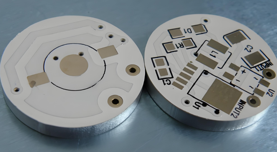
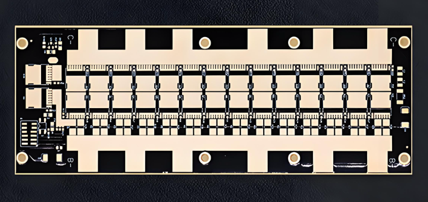
Looking for a metal core PCB design for manufacturability guide? This guide covers material selection, stackup, routing and wiring techniques, pads and solder mask, silkscreen and marking design consideration for metal core PCB production.
Are you troubled with these issues?
- How to solve device overheating when thermal efficiency is compromised?
- Who ensures the right choice of aluminum or copper core to avoid doubled costs from material mismatch?
- Who safeguards mass production timelines when lead times are repeatedly delayed?
As a professional metal core PCB manufacturer, EBest Circuit (Best Technology) can provide you service and solutions:
- Thermal Path Customization: Based on 3000+ case databases, precisely match core thickness and copper foil layers to ensure ≤45°C temperature rise at 1W power, boosting thermal efficiency by over 40%.
- Material Adaptation Expert Team: Our 20-year experienced engineers manually review and provide optimal aluminum/copper core solutions based on power density, weight constraints, and cost budgets, eliminating material selection errors and saving 15%-30% in costs.
- 7-Day Rapid Delivery Promise: Full-process green channels with pre-laminate + precision drilling technology, reducing standard board lead times to 7 days and complex multi-layer boards to ≤14 days, with real-time progress tracking.
Welcome to contact us if you have any request for metal core PCB: sales@bestpcbs.com.
Metal Core PCB Material Selection Guide: Aluminum Core vs Copper Core
A Detailed Selection Guide to Metal Core PCB Material:
1. Aluminum PCB Features and Suitable Scenarios
- Thermal Conductivity: Typically 1–2 W/m·K, meeting most medium-to-low power heat dissipation needs.
- Cost Advantage: Low raw material prices and mature processing technology, resulting in overall manufacturing costs 30%–50% lower than copper PCBs.
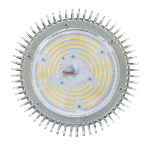
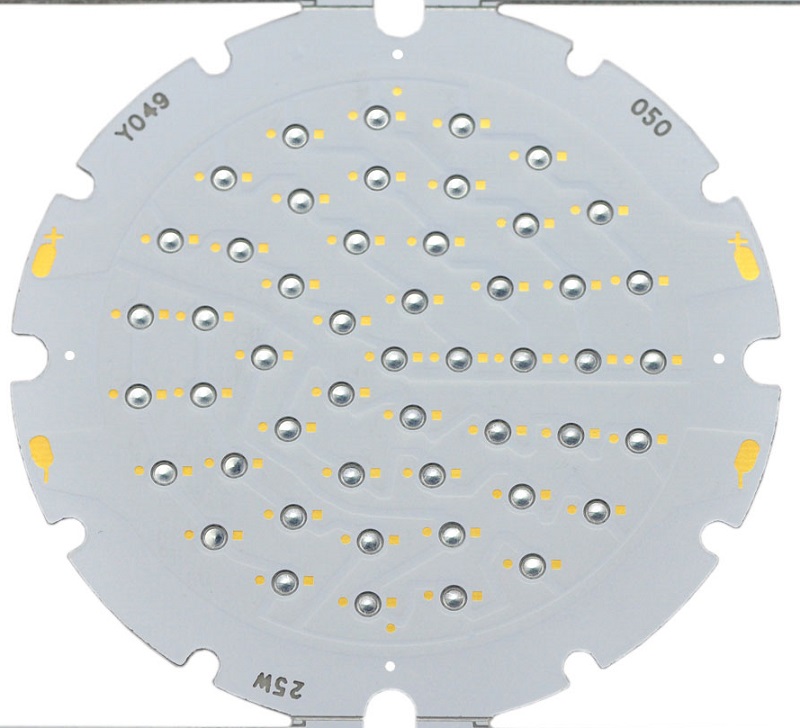
- Weight and Processing: Low density (≈2.7 g/cm³), easy to cut and punch, suitable for large-area or weight-sensitive devices (e.g., LED light panels, automotive displays).
2. Copper PCB Features and Suitable Scenarios
- Thermal Performance: Thermal conductivity up to 3–4 W/m·K, providing excellent heat paths for high-power density devices (e.g., power modules, laser drivers).
- Mechanical and Electrical Performance: High strength and better current-carrying capacity, but heavier (≈8.9 g/cm³) and significantly more expensive than aluminum PCBs.
- Typical Applications: High-frequency power supplies, military electronics, server motherboards, and other scenarios with extremely strict heat dissipation requirements.
3. Insulation Layer Selection Key Points
- The thermal insulation layer should use materials with thermal conductivity of 1–3 W/m·K and dielectric strength >2 kV (e.g., epoxy-based or ceramic-filled materials) to ensure reliable heat transfer and electrical isolation.
4. Copper Foil Thickness Selection Guide
- Conventional Scenarios: 1 oz (35 μm) copper foil meets most routing needs.
- High Current/High Power Scenarios: Increase to 2–4 oz (70–140 μm) to reduce line resistance and temperature rise.
5. Comprehensive Comparison Table: Aluminum vs Copper Core
| Item | Aluminum PCB | Copper PCB |
| Thermal Conductivity (W/m·K) | 1–2 | 3–4 |
| Cost | Low | High (Approx. 2–3 Times) |
| Weight | Light | Heavy |
| Processing Difficulty | Easy | Difficult (Requires Special Tooling) |
| Suitable Power | Medium-to-Low | High |
How to Choose the Right Metal Core PCBs Stackup and Thickness?
A Comprehensive Selection Guide to Metal Core PCB Stackup and Thickness:
1. Clarify Application Scenarios and Core Requirements
- For thermal management priority scenarios (e.g., LED lighting, power modules), choose aluminum/copper substrates with high thermal conductivity (thermal conductivity ≥1W/(m·K)). Adopt a sandwich structure of “metal substrate + insulating layer + copper foil” with insulating layer thickness controlled at 50-200μm to balance thermal resistance and electrical performance.
- For high-frequency signal scenarios (e.g., 5G RF modules), use low-loss insulating materials (e.g., PTFE, ceramic-filled epoxy resin). Stack-up design focuses on impedance matching, with copper foil thickness recommended at ≥35μm to reduce signal loss.
- For mechanical strength demand scenarios (e.g., automotive electronics, industrial control), select copper substrates (CTE close to silicon chips) or aluminum substrates (lightweight). Substrate thickness must be ≥1.5mm to resist vibration and impact.
2. Golden Rules for Stack-up Structure Design
- Single-layer MCPCB: Suitable for simple circuits, low cost but with a single heat dissipation path. Ensure heat-generating components are in direct contact with the metal substrate.
- Double-layer/multi-layer MCPCB: Adopt a structure of “metal substrate + multi-layer insulating layers + multi-layer copper foils” with vertical interconnection via buried/blind vias, ideal for complex circuit designs. Note that interlayer insulating materials must be compatible with high-temperature soldering (Tg ≥170°C).
- Hybrid stack-up design: Embed copper blocks or heat pipes locally into the metal substrate to form “active heat dissipation zones” for localized hot spot cooling needs.
3. Refined Strategies for Thickness Selection
- Substrate thickness: Aluminum substrate thickness ranges from 0.8mm to 3.2mm, copper substrate thickness from 0.5mm to 2.0mm. Select based on balancing thermal dissipation and mechanical strength. For example, high-power LED modules commonly use 1.6mm aluminum substrates, while aerospace-grade equipment may use 0.8mm copper substrates for weight reduction.
- Copper foil thickness: Standard choices are 35μm (1oz) and 70μm (2oz). For high-current scenarios, use ≥105μm (3oz) copper foil. Note that thicker copper foil increases cost and processing difficulty.
- Insulating layer thickness: Must pass dual verification via thermal resistance calculation and electrical breakdown testing. For instance, a 100μm insulating layer must meet 500MΩ insulation resistance requirements under 2000V voltage.
4. Synergistic Optimization of Key Process Parameters
- Thermal expansion coefficient (CTE) matching: The CTE of the metal substrate must be close to that of chips/devices (e.g., silicon CTE is 2.6ppm/°C) to avoid solder joint cracking due to thermal cycling. Copper substrates (17ppm/°C) are closer to silicon, while aluminum substrates (22ppm/°C) require process optimization to compensate for differences.
- Surface treatment processes: Electroless Nickel Immersion Gold (ENIG) is suitable for fine-pitch pads, while Hot Air Solder Leveling (HASL) is suitable for high-current paths. Choose based on soldering processes.
- Design for Manufacturability (DFM): Evaluate parameters such as drilling accuracy (minimum hole size 0.2mm), trace width/spacing (minimum 3mil), and solder mask coverage in advance to ensure design manufacturability.
5. Closed-Loop Management of Verification and Testing
- Thermal simulation verification: Use tools like ANSYS to simulate temperature distribution and ensure maximum junction temperature stays below chip specification limits (typically ≤125°C).
- Electrical performance testing: Include real-world verification of dielectric constant (Dk) and loss tangent (Df), with a focus on high-frequency scenarios.
- Reliability testing: After completing thermal shock (e.g., -40°C~125°C for 1000 cycles) and vibration tests (e.g., random vibration at 5g RMS), perform X-ray inspection to check solder joint integrity.
Best Practice for Metal Core PCB Layout & Routing
1. Thermal Management-Driven Layout Strategies
- Concentrated Layout of Heat-Generating Components: Place high-power devices (e.g., power transistors, LED chips) at the center of the metal substrate to leverage its high thermal conductivity for rapid lateral heat diffusion, avoiding local hot spots.
- Direct Heat Dissipation Path Design: Ensure direct contact between heat-generating components and the metal substrate. Minimize insulation layer thickness or use thermal via arrays (e.g., 1.0mm pitch) to enhance thermal conduction efficiency.
- Thermal Isolation Zoning: Physically separate sensitive components (e.g., analog circuits, high-frequency modules) from heat-generating components using etched grooves or insulation barriers on the metal substrate to prevent thermal interference-induced performance drift.
2. Signal Integrity and Routing Optimization
- High-Frequency Signal Routing Rules: For 5G/RF high-frequency scenarios, adopt “short and straight” routing to avoid bends or crossings. Use differential pair routing (strictly matched trace width/spacing) to control impedance (e.g., 50Ω microstrip lines) and reduce signal reflection/crosstalk.
- High-Current Path Optimization: Design high-current paths (e.g., power rails) with “thick copper + wide traces” (copper thickness ≥105μm, trace width ≥200mil). Embed copper bars or metal busbars to enhance current-carrying capacity, leveraging the metal substrate’s low impedance.
- Grounding and Shielding Design: Utilize the metal substrate as a natural ground plane. Implement star grounding to minimize ground bounce noise. For high-frequency sensitive circuits, use ground via arrays to form Faraday cages, suppressing EMI.
3. Mechanical Strength and Assembly Compatibility
- Component Layout Stress Balancing: Position heavy components (e.g., inductors, transformers) near the substrate center or support structures to avoid edge stress concentration. Validate deformation within safety thresholds via FEA under vibration/impact.
- Assembly Process Adaptation: Account for soldering/press-fit assembly requirements. Ensure SMD pads maintain ≥0.2mm clearance from the metal substrate. Reserve mechanical allowances for through-hole components to prevent drilling deviations affecting electrical performance.
- Maintainability Design: Place critical test points (e.g., power/signal nodes) at substrate edges or accessible areas for ICT/fault diagnostics. Reserve adequate space in repair zones to avoid tool operation constraints.
4. Reliability Verification and Process Control
- Thermal Cycling Test Validation: Verify solder joint reliability via -40℃~125℃ thermal shock cycles (≥1000 cycles). Use X-ray/C-SAM scanning to detect voids/cracks.
- Electrical Performance Measurement: Conduct TDR testing on critical signal paths to ensure impedance matching. Measure S-parameters (e.g., S11/S21) in high-frequency bands to validate signal integrity.
- Process Window Control: Collaborate with PCB manufacturers to define metal substrate processing parameters (e.g., flatness ≤0.1mm, burr height ≤10μm) and surface finishes (e.g., ENIG/OSP) for mass production feasibility.
5. Thermal Management-Driven Layout Strategies
- IPC Standards Adherence: Reference IPC-4101B (substrate materials) and IPC-6012D (rigid PCB performance) to meet mechanical/electrical/thermal requirements.
- Industry Certification Alignment: For automotive/aerospace high-reliability sectors, comply with AEC-Q200 (passive components) and AS9100 (aerospace quality systems) for market access.
- Documentation and Traceability: Provide complete design documentation (Gerber/BOM), process specifications, and test reports to support customer audits/traceability, enhancing design transparency and trust.
Metal Core PCB Pads and Solder Mask Design Considerations
1. Pad Size and Heat Dissipation Path Optimization
- High-Power Device Pad Design: For power modules (e.g., MOSFET, IGBT), adopt “extended pad” structures by increasing pad area (≥200% of the device’s base area) to reduce thermal resistance. Combine with the metal substrate’s high thermal conductivity to form vertical heat dissipation channels. For example, LED package pads often use dual-zone designs (thermal pad + signal pad), where the thermal pad directly contacts the metal substrate to enhance heat diffusion efficiency.
- Thermal Via Array Configuration: Deploy high-density thermal vias (e.g., 0.3mm diameter, 1.0mm pitch) in the pad area. Fill vias with thermally conductive materials (e.g., silver paste) to boost heat conduction and prevent local hot spots from causing solder joint cracking.
- Insulation Isolation and Creepage Distance: Maintain ≥0.2mm insulation clearance between pads and the metal substrate. Use high-voltage-resistant insulation materials (e.g., PI tape, ceramic coatings) to meet safety creepage distance requirements (e.g., ≥2.5mm/kV) in high-voltage scenarios (e.g., power modules).
2. Pad Size and Heat Dissipation Path Optimization
- Solder Mask Thickness Control: Standard solder mask thickness should be 20-30μm; for high-abrasion scenarios (e.g., automotive electronics), increase to 50μm to enhance mechanical damage resistance. Balance thermal resistance and electrical performance to avoid excessive thickness impairing heat dissipation efficiency.
- Solder Mask Material Matching: Select high-temperature-resistant solder mask inks (Tg≥170℃) to withstand reflow soldering peak temperatures (260℃). Verify chemical corrosion resistance (e.g., flux residue cleaning) and UV aging resistance.
- Solder Mask Opening Optimization: Opening dimensions should exceed pad size by 0.1-0.2mm to accommodate solder paste printing tolerances. Avoid excessive proximity between opening edges and adjacent conductors to prevent short-circuit risks. For BGA devices, use “negative mold” designs to ensure accurate solder ball placement.
3. CTE Matching and Stress Management
- Pad Material Selection: Prioritize materials matching the metal substrate’s CTE (e.g., copper-based pads ≈17ppm/℃, aluminum-based pads ≈22ppm/℃) to minimize solder joint fatigue failure from thermal cycling.
- Stress Relief Structure Design: Deploy “stress relief grooves” or “flexible connection bands” around pads. Use localized substrate thinning or elastic buffer layers (e.g., silicone) to absorb thermal stress and improve soldering reliability.
- Solder Alloy Optimization: For high-reliability scenarios, recommend lead-free SAC305 (Sn96.5Ag3Cu0.5) solder with a melting point (217℃) compatible with the metal substrate’s thermal expansion characteristics, offering good mechanical strength and creep resistance.
4. Electrical Insulation and Breakdown Protection
- Insulation Layer Thickness Verification: Calculate minimum insulation layer thickness using the “voltage gradient method” (e.g., ≥100μm for 2000V scenarios) and validate via voltage withstand tests (e.g., AC 2500V/1min) to prevent arc breakdown from insufficient insulation.
- Edge Effect Protection: Use “rounded corner” designs on pad edges to reduce electric field concentration. Combine with solder mask coverage for dual insulation protection. For high-voltage scenarios, add “shielding ring” structures to disperse electric field intensity.
- Tracking Resistance Protection: Select solder mask materials with high CTI (Comparative Tracking Index) ≥600 and apply conformal coatings (e.g., acrylic, polyurethane) to enhance surface insulation resistance and prevent moisture-induced leakage failures.
5. Electrical Insulation and Breakdown Protection
- Pad Pitch and Solderability: Minimum pad pitch ≥0.2mm to align with SMT placement accuracy. Verify solder paste printing uniformity (e.g., 3D SPI inspection) and reflow peak temperature profiles (e.g., 245±5℃) for soldering quality.
- Surface Finish Adaptation: Choose surface finishes based on soldering processes—ENIG for fine-pitch pads (e.g., 0.4mm pitch BGA), HASL for high-current paths, OSP for cost-sensitive scenarios.
- Automated Assembly Compatibility: Designs must integrate with automated equipment (e.g., pick-and-place machines, AOI systems). Ensure pad dimensions match nozzle pickup ranges and solder mask openings avoid reflection interference for optical inspection.
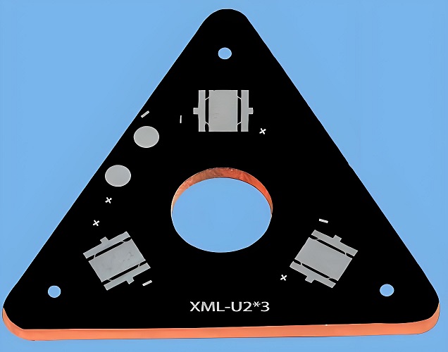
Metal Core PCB Silkscreen and Marking Design Specifications
| Design Element | Specification |
| Silkscreen Ink | High-temperature epoxy ink (≥280°C), UV ink prohibited |
| Character Size | Minimum height: 1.2mm, line width ≥0.15mm, aspect ratio 1:5 |
| Polarity Marking | symbol diameter ≥2mm, +/- symbols 20% bold, solid square for Pin1 |
| Thermal Zone Warning | lightning symbol + HIGH TEMP ZONE, text ≥0.5mm from copper foil |
| Barcode/QR Code | Minimum size 8x8mm, clearance ≥20% of code width, contrast >60% |
| Certification Marks | UL logo diameter 3±0.2mm, CE height ≥1.5mm, ≥2mm from board edge |
| Environmental Resistance | 3 validations: 85℃/85%RH 500h, 48h salt spray, 50x alcohol wipe |
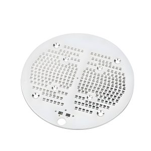
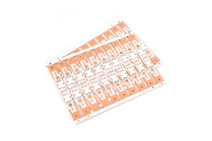
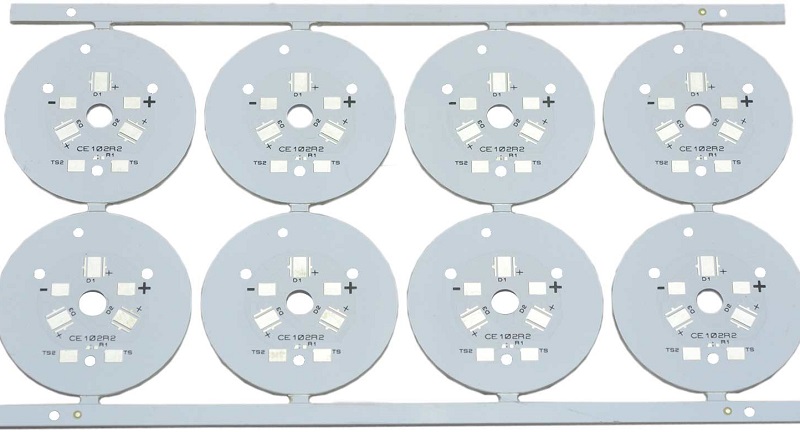
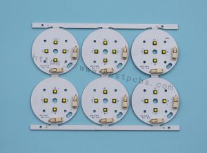
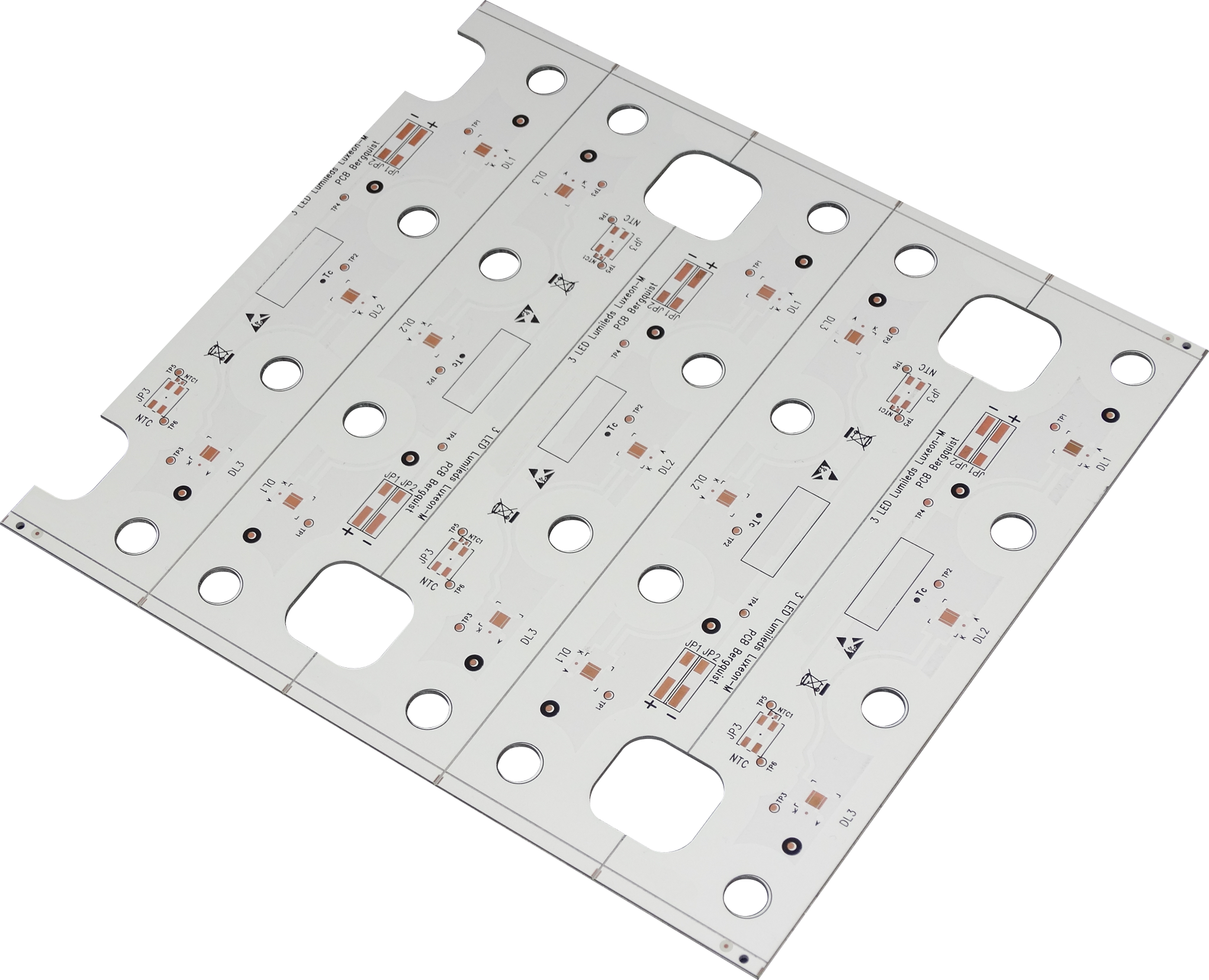
MCPCB Panelization and Process Edge Design Practical Guide
1. Panel Layout Optimization:
- Single board arrangement logic: Use matrix arrangement with ≥2.0mm spacing between boards, reserve connection bridges (width 1.5-2.0mm) to enhance mechanical strength. For large boards (≥50×50mm), adopt “Field” shaped symmetric layout to reduce thermal stress concentration during soldering.
- Depanelizing method selection: Prioritize V-cut scoring (depth controlled at 1/3 of board thickness) or laser scoring to avoid burrs from mechanical punching. Post-depaneling edge flatness must be verified (burr height ≤0.1mm).
- Panel size compatibility: Panel outer frame dimensions must align with customer SMT production line standard carriers (e.g., 330×250mm or 460×360mm). Edge process margins ≥5.0mm are required for clamping and conveyance.
2. Process Edge Functional Area Design
- Clamping and positioning zones: Set ≥8.0mm width clamping zones on all four edges. Use non-plated holes (diameter 3.0mm) or plated positioning holes (spacing 10.0mm) compatible with automated fixtures. Edge textures (depth 0.2mm) should be added to prevent slippage during assembly.
- Test point layout: Centralize ICT test points (spacing ≥2.5mm) on process edges with probe diameter ≥0.7mm and ≥70% contact area. High-voltage test points require red warning frames + lightning symbols per IEC 60664 safety standards.
- Identification and traceability zones: Fix QR codes/batch numbers (size ≥4×4mm) in edge zones via laser engraving with ≥30% error correction. Safety certification marks (CE, UL) must be placed in unobstructed areas with character height ≥1.0mm for 100% AOI recognition.
3. Thermal Management and Heat Dissipation Path Design
- Heat dissipation channel planning: Reserve thermal via arrays (spacing ≤1.0mm) in connection bridge areas with ≥25μm copper plating thickness. Direct heat paths from component pads to metal core should be ensured. For high-power components (e.g., MOSFETs), add solid copper blocks (area ≥120% of component projection).
- Edge heat dissipation design: Process edge zones require heat sink mounting positions (e.g., M3 screw holes) with ≥3.0mm distance from metal core edges to prevent thermal expansion-induced cracks. Anodized heat sinks are recommended for enhanced corrosion resistance.
4. Process Compatibility and Standardization
- Lamination process compatibility: Verify compatibility between metal substrates and PCB lamination processes to prevent blistering/delamination at lamination temperatures (180-200°C). Edge overflow grooves (width 0.5mm) should be added to prevent resin contamination on process edges.
- Eco-friendly ink selection: Screen printing inks must withstand ≥3 reflow cycles (260°C peak), 72h 5% NaCl salt spray corrosion, and comply with RoHS 2.0/REACH. UV-curable epoxy inks are recommended.
- Standardized file output: Provide Gerber panel layers (Panel Layer) and process edge layers (Process Edge Layer) for global supply chain consistency. Designs must comply with IPC-SM-840C silkscreen standards with ≥0.25mm character spacing and no connected strokes.
5. Assembly and Testing Friendliness
- Component marking clarity: Component markings must be ≥0.5mm from pads to prevent AOI misjudgment during SMT. Polarity symbols (+, -) require ≥0.2mm line width to avoid blurring at high temperatures.
- Mistake-proofing design: Add mistake-proofing grooves (depth 0.5mm) or shaped holes in critical edge zones to prevent orientation errors. High-voltage zones need red warning frames + lightning symbols to reduce mis-touch risks during maintenance.
- Test point accessibility: Test points must avoid burr areas at metal core edges with ≥70% probe contact area. ICT fixtures must align with panel dimensions for precise positioning and reduced false touches.
Metal Core PCB Design for DFM Checklist
1. Substrate Selection and Compatibility Verification
- Prioritize high-thermal-conductivity aluminum/copper/iron-based composite materials; verify CTE match with component packages to prevent thermal stress-induced delamination.
- Substrate thickness must meet thermal dissipation requirements (e.g., ≥1.0mm aluminum for high-power LED modules) and maintain dimensional stability under peak reflow temperature (260°C).
2. Thermal Management Design Compliance
- Critical heat-generating components (e.g., MOSFETs, ICs) must be directly mounted on the metal core; thermal paths should be short and direct, avoiding thermal resistance ≥5°C/W.
- Thermal via arrays must be uniformly distributed (spacing ≤1.0mm) with copper plating thickness ≥25μm for efficient heat conduction.
- Surface heat sink/mounting positions require pre-set alignment holes and anti-slip textures to accommodate automated assembly lines.
3. Screen Printing and Marking Optimization
- Component markings use high-contrast colors (e.g., white/black on aluminum substrate); character height ≥0.8mm, polarity symbols (+, -) line width ≥0.2mm.
- Safety certification marks (CE, UL) and high-voltage warning symbols must be placed in fixed board-edge areas to avoid shielding by heat sinks.
- Batch numbers/QR codes use laser engraving; size ≥3×3mm, error correction rate ≥30% for traceability after transport wear.
4. Process Compatibility Verification
- Verify compatibility between metal substrates and PCB lamination processes to prevent blistering/delamination at lamination temperatures (180-200°C).
- Solder pad design must suit lead-free solder (e.g., SAC305); pad spacing ≥0.5mm to prevent solder bridging.
- Test points (e.g., ICT probe points) must avoid burr areas at metal substrate edges; probe diameter ≥0.7mm for reliable contact.
5. Environmental Adaptability Design
- Inks must withstand ≥3 reflow cycles (260°C peak), 72h 5% NaCl salt spray corrosion, and solvent resistance (e.g., flux cleaning).
- Comply with RoHS 2.0/REACH; prohibit heavy metals (Pb/Cd); use UV-curable eco-inks.
- ESD markings use yellow background with black text; high-voltage areas use red warning frames + lightning symbols per IEC 60664.
6. Standardization and Traceability
- Follow IPC-SM-840C screen printing standards; character spacing ≥0.25mm, avoid connected strokes.
- Provide Gerber silkscreen layers (GTO/GBO) for global supply chain design consistency.
- Implement batch/QR code lifecycle traceability to meet ISO 13485 (medical) certification.
7. Assembly and Testing Friendliness
- Component markings ≥0.5mm from pads to prevent AOI misjudgment during SMT.
- Critical markings in fixed board-edge areas optimize DFA (Design for Assembly).
- Test point layout compatible with customer ICT/FCT fixtures; probe contact area ≥70% to reduce false touches.
Please feel free to contact us if you have any request for metal core PCB: sales@bestpcbs.com.