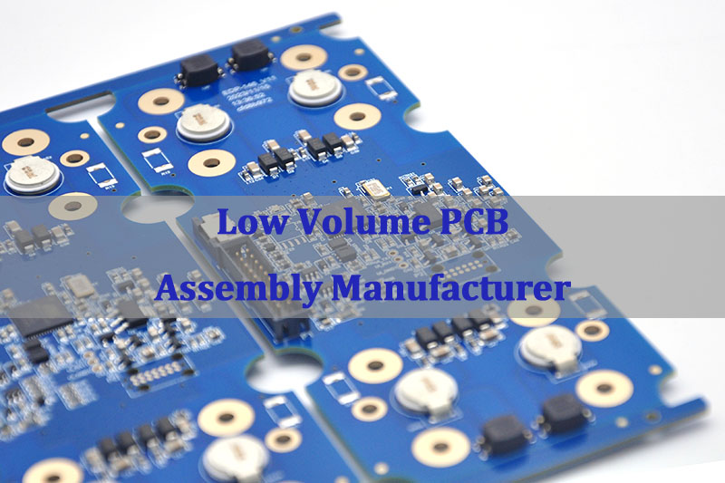
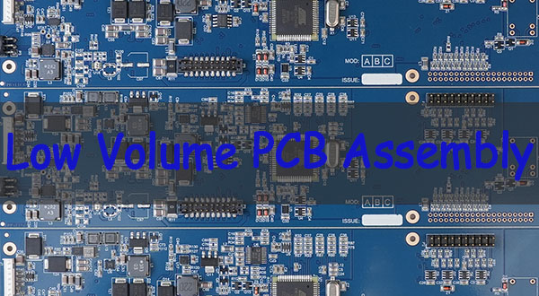
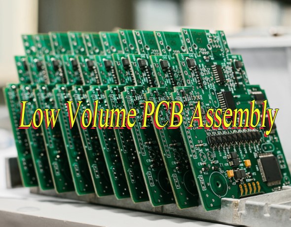
Struggling to find reliable low volume PCB assembly for small-batch projects? For teams navigating small-batch electronic production, consistent, high-quality low volume PCB assembly is often the biggest roadblock between prototype testing and full market launch.
EBest Technology delivers targeted low volume PCB assembly solutions to eliminate this gap entirely, with zero compromise on quality or speed. As a China-based professional manufacturer with 19+ years of dedicated PCBA expertise, we specialize in small-volume, prototype-focused assembly that skips strict mass-production minimums. We maintain strict quality controls and support fast turnaround for critical projects across medical, aerospace, and industrial equipment sectors. And we cut unnecessary delays and hidden costs, focusing on functional, compliant small-batch PCBA that meets global industry standards reliably.
What Are Low Volume PCB Assembly Services?
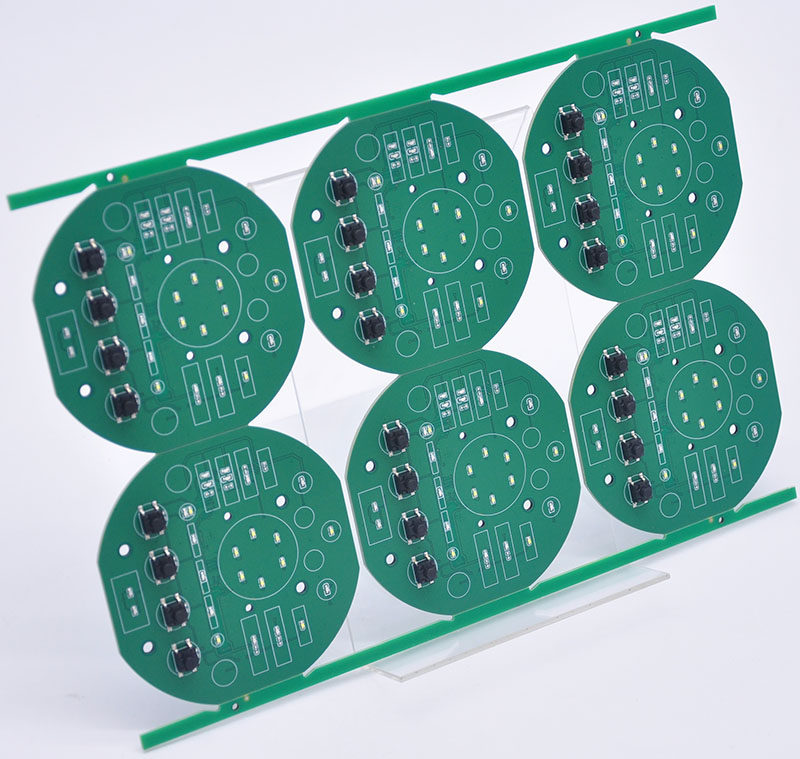
Low volume PCB assembly refers to specialized printed circuit board assembly services designed for small production runs, typically ranging from single prototype units to low thousands of finished boards, filling the critical gap between initial prototype development and full-scale mass manufacturing. Unlike mass production facilities that enforce high minimum order quantities (MOQs) and prioritize large-batch efficiency, this service caters to niche product testing, custom industrial equipment builds, medical device validation, aerospace component prototyping, and small-market product launches.
This targeted assembly model supports flexible order sizes, personalized production adjustments, and rigorous quality checks for every unit, making it ideal for projects that require precision, compliance, and speed without the expense of large-scale production. Every long tail keyword tied to small-batch assembly aligns with this core definition, including prototype PCB assembly services low volume and small volume PCB assembly.
Stuck Between Prototype and Mass Production? Our Services Are the Solution.
Finding reliable low volume PCB assembly is critical for bridging prototype and mass production. EBest provides targeted solutions for small-batch projects, with no high MOQs, strict quality controls, and fast turnaround. We serve medical, aerospace, and industrial equipment sectors, ensuring compliant, high-quality boards without unnecessary delays or hidden costs. Our in-house fabrication and component sourcing eliminate external supply chain risks, supporting seamless scaling from validation to limited production runs.
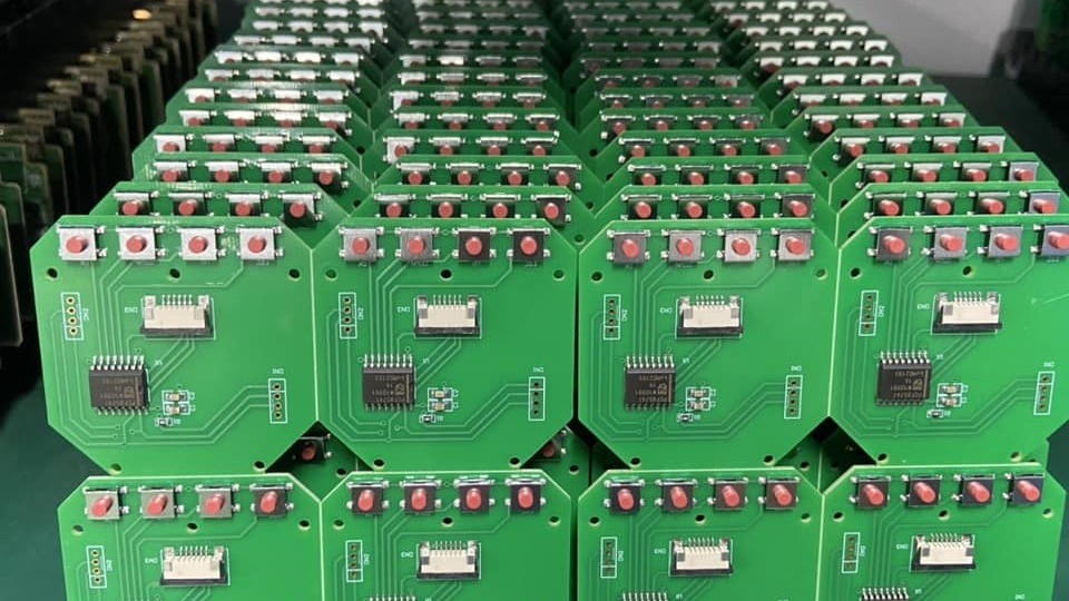
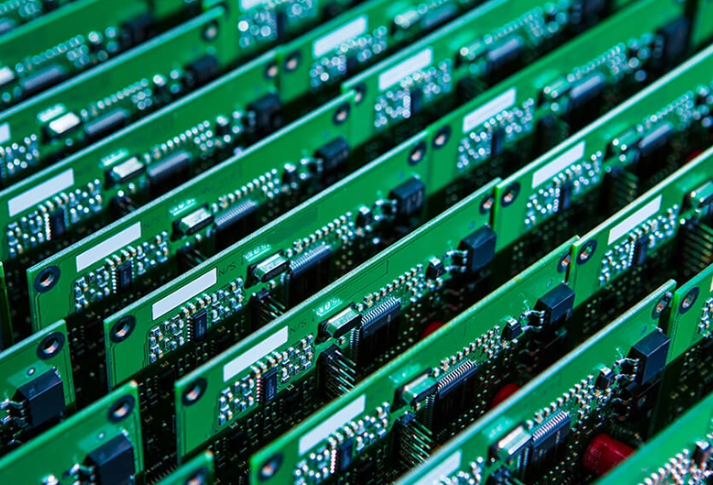
As a leading low volume PCB assembly manufacturer in China, EBest stands out with 19+ years of expertise, global certifications (ISO 13485, AS9100D, IATF 16949) and advanced automation. We offer a full range of services: prototype assembly, quick-turn solutions, full turnkey support, precision BGA, through-hole, flex/rigid-flex, and ceramic PCB assembly. Our capabilities include 13.2 million chips daily placement, 1-5 day standard lead times, and 24-hour rush service, with 100% full inspection before shipment. We also provide cost-saving strategies, such as consolidating small orders and using standard components, to optimize budgets without compromising quality.
Is Your Budget Tight? How to Save on Small Volume PCB Assembly?
Tight budgets often derail low volume circuit board assembly projects, from prototype validation to small-batch medical and industrial runs. Most teams overspend by 25%-35% on small orders, thanks to unoptimized workflows, hidden setup fees, and inflated middleman markups that punish low-quantity buyers.
Even small, one-off prototype batches face unfair premium pricing, and these extra costs quickly eat into project budgets and delay product development timelines for niche and specialized electronic builds.
As a professional China low volume PCB assembly factory, EBest cuts your total low volume PCB assembly costs by 20%-40% compared to standard manufacturers, with clear, actionable cost-saving methods. Our in-house PCB fabrication and direct component supply chain remove middleman fees entirely, slashing material and sourcing costs by 15%-20% for small batches.
We also optimize production setup and panelization for small orders, cutting per-unit setup and labor expenses by another 10%-20%, so you pay fair prices even for tiny batch sizes with no hidden charges.
We never sacrifice quality to lower costs, our streamlined small-batch workflows reduce waste and redundant steps, not performance. We offer free design-for-manufacturing (DFM) checks to avoid costly reworks, which can save you an extra 10%-15% on post-production fixes.
Our consistent, defect-controlled assembly also eliminates costly replacement orders, letting you stay within budget while getting reliable, production-ready boards for medical, aerospace, and industrial applications.
Does Low Volume Mean Lower Quality? Ensuring Excellence in Every Batch.
A common misconception about low volume PCB assembly services is that small batches mean lower quality standards, and this worry often stalls critical small-batch projects. At EBest, we eliminate this concern with strict, repeatable production controls and data-backed quality performance, tailored specifically for low volume and prototype orders.
We treat every small-batch order with the same rigorous process discipline as high-volume runs, with standardized operating procedures for every assembly step, no matter how small the order quantity. Our 19+ years of PCBA experience lets us lock in consistent quality without cutting corners or rushing production for quick turnaround.
We run full incoming material inspections for every batch, verifying raw PCB substrate quality and component authenticity before assembly starts. We only use A-grade, wear-resistant materials, and reject any subpar incoming parts to prevent defects early in the process.
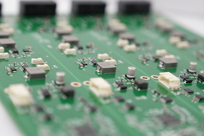
Our automated SMT placement equipment runs calibrated precision checks before each batch, maintaining consistent placement accuracy even for tiny 01005 SMD components and 0.25mm pitch BGA packages. This machine calibration eliminates human error and ensures uniform quality across every unit.
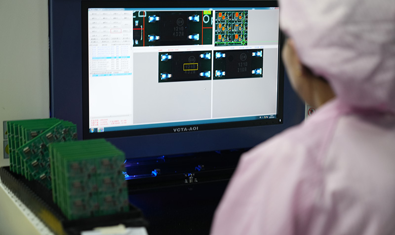
We enforce 100% full inspection on every assembled board before shipment, including automated optical inspection (AOI), soldering integrity checks, and functional performance testing where required. Our quality data confirms a defect rate of less than 0.3% for all low volume batches, matching the reliability of large-scale production.
Defective units are immediately isolated and reworked or scrapped, with zero substandard boards leaving our facility. We also conduct post-assembly stability checks for boards used in high-demand environments, ensuring long-term durability.
Our low volume assembly has been validated for real-world use across medical diagnostic tools, aerospace control components, and heavy-duty industrial equipment. These applications demand consistent, reliable performance, and our small-batch boards pass field testing and operational stress checks without quality gaps.
This track record proves low volume assembly never means lower quality, it simply means targeted, precise production that prioritizes consistency and reliability for your specialized, small-scale projects.
Urgent Need Assembled Boards? How We Accelerate Your Low Volume PCB Assembly
Missed deadlines for small-batch PCB orders can derail your entire project timeline, push back product launches, and even disrupt critical emergency operations. That’s why PCB assembly low volume orders need fast, dependable turnaround you can count on, not vague delivery promises.
EBest’s dedicated expedited production system delivers on urgent requests reliably: we can ship fully assembled, inspected boards within 24 hours for your most time-sensitive projects. Our in-house PCB fabrication and component sourcing teams cut out third-party delays entirely, and our automated assembly lines speed up processing without sacrificing placement precision or soldering quality.
For most standard low volume projects, our regular lead time is just 1–5 business days, far faster than industry averages for small-batch assembly. We’ve supported countless urgent requests: emergency medical device repairs, tight aerospace prototype testing windows, and last-minute industrial equipment replacement parts, helping clients hit critical deadlines without compromising on board quality.
Struggling with Parts? Our Component Sourcing for Circuit Board Assembly.
Few hurdles slow down low volume PCB assembly projects more than frustrating component sourcing struggles. Most buyers face endless hours hunting for small-batch parts, steep price markups for low-quantity orders, strict supplier MOQs that block small purchases, and constant fear of counterfeit or low-quality components derailing production entirely.
These roadblocks don’t just waste time, they push back project deadlines, inflate total costs, and create unnecessary stress for critical small-batch builds, from medical device prototypes to aerospace test components and industrial equipment replacements.
At EBest, we eliminate every one of these pain points with our dedicated, full-coverage component sourcing service, built exclusively to support low volume PCB assembly services and small-batch production needs. We take the entire parts procurement burden off your plate, so you can focus on project progress instead of supply chain headaches.
Our global, stable component supply chain covers every standard and specialty part you need, including SMD, BGA, QFN, QFP, and through-hole components, with no unfair small-order penalties. We vet every supplier rigorously to guarantee 100% authentic, high-quality components, eliminating counterfeit risks entirely for your sensitive industrial, medical, and aerospace projects.
We also leverage our 19+ years of industry partnerships to lock in competitive pricing for low-quantity parts, cutting your component costs by up to 20% compared to independent sourcing. No more haggling, no more delayed deliveries, and no more stalled production, just reliable, timely, cost-effective parts that keep your low volume PCB assembly project on track and on budget, from start to finish.
Why is a China-Based Factory Like EBest Your Best Choice?
Choosing a trusted low volume PCB assembly manufacturer in China means accessing cost efficiency, advanced technology, and global compliance, and EBest stands out as a leader with 19+ years of specialized experience. Below are the core advantages that make us the best partner for your small-batch PCBA needs:
- 19+ years of dedicated PCB and PCBA manufacturing expertise, serving global clients across medical, aerospace, and industrial sectors
- Full suite of global quality certifications (IATF 16949, ISO 9001, ISO 13485, AS9100D, RoHS, UL) for regulatory compliance.
- In-house PCB fabrication and component sourcing, offering full turnkey solutions to streamline production.
- No high MOQs, catering specifically to prototype, low volume, and small-batch assembly projects.
- Advanced automated assembly equipment with 13.2 million chips daily placement speed for precision and speed.
- 100% full inspection on every assembled board before shipment, zero quality shortcuts for small batches.
- Expedited 24-hour rush service for urgent low volume orders, with standard 1-5 day lead times.
- Monthly production capacity of 260,000 square feet, handling over 1,000 unique board designs monthly.
- Customizable substrate and material options for ceramic, flex, rigid-flex, and high-frequency PCBs.
- Dedicated personalized support team for every client, with end-to-end project tracking and transparency.
What Types of Low Volume PCB Assembly Services Does We Offer?
EBest offers a complete portfolio of low volume pcb assembly services to cover every small-batch and prototype need, with specialized support for unique board types and assembly requirements. Below are types of low volume PCB assembly services we offer you:
- Prototype PCB Assembly: Custom prototype builds for design validation, testing, and regulatory approval across medical and aerospace industries.
- Quick Turn PCB Assembly: Fast-turnaround small-batch assembly for urgent project deadlines and emergency replacement parts.
- Full Turnkey PCB Assembly: End-to-end service including PCB fabrication, component sourcing, assembly, and full inspection.
- BGA Assembly: Precision BGA assembly with 0.25mm minimum pitch, ideal for high-density industrial and aerospace electronics.
- Through-Hole Assembly: Reliable through-hole component assembly for rugged industrial equipment and high-durability applications.
- Flex & Rigid-Flex PCB Assembly: Specialized assembly for flexible circuit boards used in medical devices and compact aerospace components.
- Ceramic PCB Assembly: High-temperature ceramic PCB assembly for industrial and aerospace applications with extreme operating conditions.
- Box Assembly: Complete box build assembly with full automation and final inspection, ready for immediate deployment.
Our Low Volume Circuit Board Assembly Capabilities
| Capability Category | Detailed Specifications |
| Placement Speed | 13,200,000 chips per day (automated precision placement) |
| Bare Board Size Range | 0.2″ x 0.2″ to 22″ x 47.5″ |
| Minimum SMD Component | 01005 (ultra-small component support) |
| Minimum BGA Pitch | 0.25mm (high-density BGA assembly capability) |
| Max Component Size | 50mm x 150mm |
| Assembly Types | SMT, Through-Hole (THT), Mixed SMT+THT Assembly |
| Component Packaging | Reels, Cut Tape, Tube, Tray, Loose Parts |
| Standard Lead Time | 1-5 business days; 24-hour rush service available |
How to Get a Quote for Your Small Volume PCB Assembly Project?
Securing a customized quote for your low volume PCB assembly project is simple and fully transparent with EBest. We’ve built a streamlined 4-step process to deliver accurate, fast pricing with zero hidden fees, so you know exactly what to expect before starting production. Follow these clear steps to launch your project smoothly:
- Submit Project Details: Send your complete PCB design files, including Gerber files, BOM list, and assembly drawings. Be sure to note your target order quantity, required lead time, and any special needs like unique substrate materials or custom assembly specs.
- Project Review & Feasibility Check: Our experienced production team reviews your design thoroughly, verifies component availability, and spots potential optimizations to improve quality or cut extra costs —no extra charge for this pre-production check.
- Custom Quote Delivery: We send a detailed, fixed quote that covers every cost: PCB fabrication, component sourcing, assembly, full inspection, and shipping. There are no surprise fees or added charges later, keeping your budget on track.
- Confirm Order & Start Production: Once you approve the quote and confirm all details, we immediately start production with full transparency, sending regular progress updates so you stay informed every step of the way.
Ready to get a hassle-free, customized quote for your low volume PCB assembly project? Don’t let budget uncertainty or project delays hold you back. Send us your project details today at sales@bestpcbs.com, and our team will respond quickly with a fair, detailed quote tailored to your needs. Whether you need prototype assembly, small-batch production, or urgent quick-turn services, we’re here to help you save costs, hit deadlines, and get reliable, high-quality boards every time.
FAQs About Low Volume Circuit Board Assembly
Q1: What is the minimum order quantity for low volume PCB assembly at EBest?
A1: We accept single prototype units, small-batch runs of 10-50 units, and mid-range low-volume orders up to a few thousand units. We cater specifically to clients who need small quantities without the high MOQs required by mass production manufacturers, making us ideal for prototype testing and niche product builds.
Q2: Are low volume PCB assembly orders subject to the same quality checks as high-volume orders?
A2: Yes, every low volume PCB assembly order undergoes 100% full inspection before shipment, including automated optical inspection (AOI), soldering quality checks, and functional testing where required. We follow the same certified quality protocols for all orders, regardless of size, and hold global certifications to ensure compliance for medical, aerospace, and industrial projects.
Q3: How long does it take to complete a standard low volume PCB assembly order?
A3: Our standard lead time for low volume PCB assembly is 1-5 business days from order confirmation. For urgent, time-critical projects, we offer a 24-hour expedited service for qualified small-batch orders, ensuring you receive finished boards exactly when you need them for testing or deployment.
Q4: Can you handle specialized PCB materials for low volume assembly?
A4: Absolutely, we support a full range of specialized PCB substrates and materials for low volume assembly, including FR4, ceramic, flex, rigid-flex, metal-based (MCPCB), and high-frequency materials. We customize substrate selection to match your project’s application, whether it’s high-temperature industrial equipment, compact medical devices, or aerospace-grade electronics.
Q5: Do you provide component sourcing for low volume orders with hard-to-find parts?
A5: Yes, our dedicated component sourcing team has a global, stable supply chain to source standard, specialized, and hard-to-find electronic components for low volume orders. We avoid counterfeit parts, secure competitive pricing even for small component quantities, and eliminate the hassle of independent parts procurement for your team.