PCB manufacturing PCB manufacturing
Home > Blog

Posts Tagged ‘HDI PCB’

High Density Interconnect PCB: Everything You Should Know
Friday, September 27th, 2024

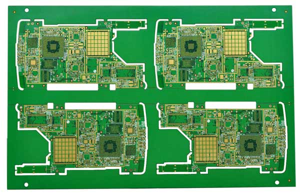
What is High Density Interconnect PCB?

High density Interconnect (HDI) PCB is a printed circuit board designed to meet the growing needs of modern electronic products. It allows for higher component density due to the use of thinner lines, smaller through-holes, and precise component placement. These boards are particularly popular in industries where miniaturization is key, such as smartphones, medical devices, and military equipment.

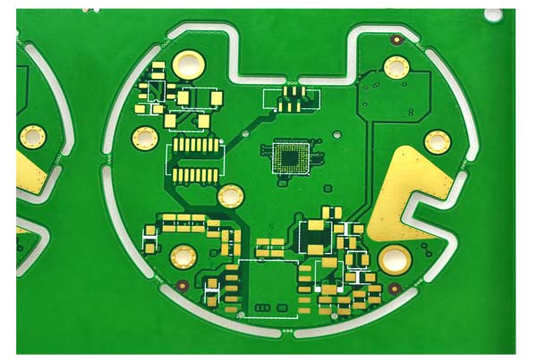
The HDI board uses the micro-blind hole technology to realize the circuit board design with high line distribution density, which is especially suitable for applications requiring high performance and high reliability. Compared with traditional PCBs, HDI boards have significant advantages in terms of volume, weight, wiring density and electrical performance, which can meet the electrical requirements of high-speed signals, provide impedance control of alternating current characteristics, high-frequency transmission capacity and reduce unnecessary radiation (EMI).

HDI PCBs use a combination of advanced technologies such as laser drilling and sequential lamination to enable denser wiring without compromising performance. By integrating smaller, more efficient through-holes, HDI boards offer greater functionality on a smaller footprint than traditional PCBs.

What is the Difference Between Connect and Interconnect?

The terms “connect” and “interconnect” may seem similar but serve distinct functions in electronics. “Connect” typically refers to the linking of two points, components, or circuits. This could be as simple as joining a wire to a terminal.

On the other hand, “interconnect” deals with more complex connections, usually involving the linking of multiple circuits or components within a system. In the context of HDI PCBs, interconnectivity is crucial because it defines how different layers and components of the board communicate. HDI technology optimizes these interconnections to make the board more efficient in terms of space and performance.

What is HDI PCB Stackup?

The stackup in HDI PCBs refers to how the multiple layers of the board are arranged. Stackups are critical in determining the board’s performance, particularly when it comes to signal integrity, power delivery, and heat dissipation. HDI stackups often involve intricate configurations that vary depending on the design’s complexity and purpose. Here are the most common types:
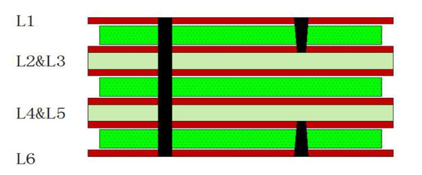
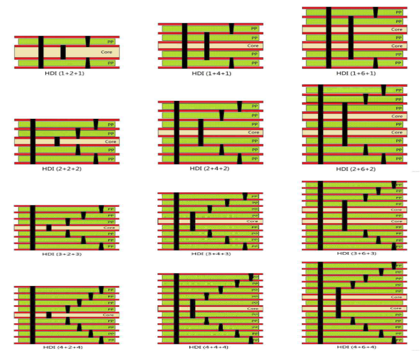
HDI PCB (1+N+1)

This is one of the simplest forms of HDI stackups, where “1+N+1” means there are two layers of high-density interconnect (one on each side) sandwiching N layers of traditional PCB. This structure is often used in applications where moderate complexity is required, providing a balance between performance and cost.
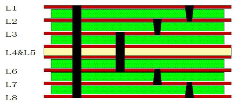
HDI PCB (2+N+2)

In this configuration, there are two HDI layers on each side of the N traditional layers. This setup allows for greater flexibility in routing, especially for complex designs requiring more components. The additional HDI layers enhance the board’s ability to manage signal transmission efficiently, making it suitable for high-performance applications.

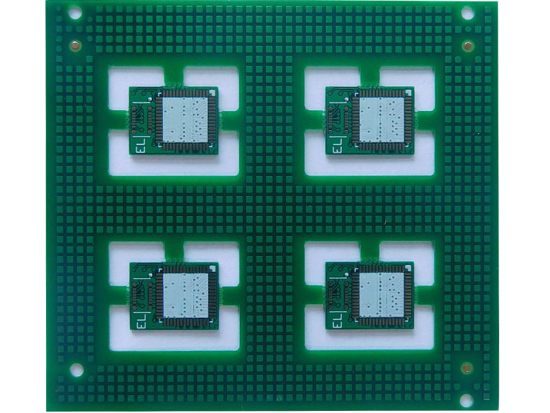
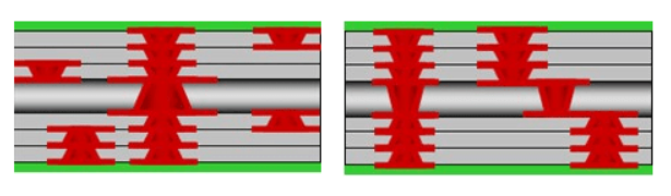
ELIC (Every Layer Interconnection): Most Complex HDI

ELIC takes HDI technology to the next level. In this configuration, every layer of the PCB can interconnect directly with any other layer. This is the most advanced form of HDI stackup, offering unparalleled design flexibility and performance. However, it is also the most complex and expensive option. ELIC is often used in cutting-edge technology applications such as aerospace and military equipment.

Other HDI Stackups

What are the Advantages of HDI PCB?

The main advantage of the HDI board is its high-density interconnect design, through the use of micro lines and highly compact layout, can achieve higher interconnection density, thereby accommodating more electronic components in a limited space, improving the performance and function of the board. This design makes HDI boards particularly suitable for applications requiring high performance and high functional density, such as high performance computing, data centers, and mobile communication equipment, to support high-speed data transmission and processing.

The design of the HDI board also focuses on improving the anti-interference ability and reliability of the circuit board, by using better signal integrity and power management technology, effectively reduce the impact of electromagnetic interference and power noise on the circuit.

However, HDI boards also have some limitations. First of all, compared with other advanced boards, the cost of HDI boards is usually lower, because HDI manufacturing technology helps to use advanced packaging technology, but its processing is more difficult, higher requirements for technology and equipment, which may increase a certain cost. In addition, the material choice of HDI board will also affect its performance and cost, such as FR4, PI and BT materials have advantages and disadvantages, need to be weighed according to the specific application needs.

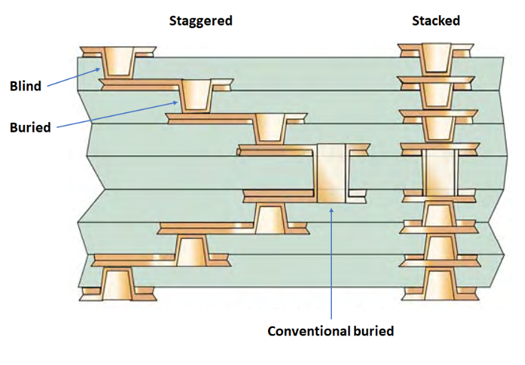
5 Types of Vias in HDI PCB

HDI PCBs rely on several types of vias to achieve their high-density interconnections. Each type of via has its specific role in the design and manufacturing process.
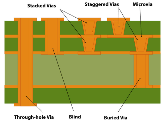
Blind Vias

Blind vias connect an outer layer of the PCB to one or more inner layers but do not extend through the entire board. These vias allow for complex routing without using unnecessary space on the PCB’s inner layers.

Buried Vias

Buried vias are located entirely within the board, connecting internal layers without appearing on the outer surfaces. This is ideal for designs where surface area needs to be preserved for components, while still allowing inter-layer connectivity.
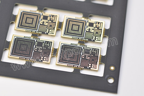
Microvias

Microvias are tiny vias, typically created using laser drilling, that connect adjacent layers of the PCB. These are essential for HDI designs as they save space while maintaining high-density connections. They can be used in stacked or staggered configurations to optimize space and signal flow.

Staggered Vias

Staggered vias are microvias that are offset from each other across layers. This design allows for more flexibility in routing and avoids overlapping, making it a popular choice for HDI PCBs that require complex routing.

Through Hole Vias

Though not exclusive to HDI designs, through-hole vias extend through the entire PCB, connecting all layers. While these vias occupy more space, they are sometimes necessary for power connections or when working with thicker boards.

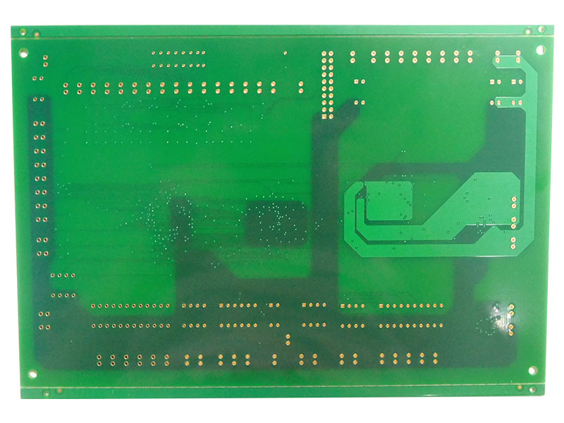
What is the Difference Between PCB and HDI PCB?

The key difference between a traditional PCB and an HDI PCB lies in the design and manufacturing process. Traditional PCBs use through-hole technology and thicker traces, limiting the board’s ability to accommodate high-density components. HDI PCBs, by contrast, use finer lines, smaller vias, and advanced interconnect techniques to maximize component density. Here are some key differences between them:

Manufacturing Processes

The embedded via and blind via technologies used in the manufacturing process of HDI (High-Density Interconnect) boards allow for the addition of more layers without increasing the thickness of the board, thereby improving space utilization. In contrast, the drilling process for standard PCBs is relatively simple, but as the number of layers increases, the board thickness also increases accordingly. This difference means that HDI boards require more advanced equipment and higher technical requirements during production.

Space Constraints

In space-constrained devices, such as smartphones and portable electronics, HDI boards are the ideal choice because they can integrate more functions within a smaller size. HDI boards can achieve a line width of 2/2 mil and a 10-layer board thickness of below 0.8mm. Standard PCBs, due to their larger size and lower integration, may not be suitable for these applications. The line width and spacing of regular PCBs are generally limited to 3/3 mil, and their thickness also has certain restrictions.

Performance Requirements

For high-end electronic products that require high-speed signal processing and complex circuit designs, HDI boards offer better performance. Due to their high density and efficiency, HDI boards can meet the high-performance demands of modern electronic devices. Standard PCBs, on the other hand, may not be suitable for these applications because of their lower signal transmission quality and higher latency.

Different Layering Methods

HDI boards are created through continuous stacking and lamination, resulting in advantages such as being “light, thin, short, and small.” Electrical interconnections between layers are achieved through conductive vias, embedded vias, and blind vias, making the structure different from standard multilayer boards. Most HDI boards are laminated two or more times (except for special structures), while standard boards are typically laminated once.

PTH vs. HDI PCB

Plated Through Hole (PTH) technology is commonly used in traditional PCBs and involves drilling holes through the entire board to connect different layers. This method, while reliable, is limited in terms of design flexibility and component density.

HDI PCBs, on the other hand, use smaller vias such as microvias, blind vias, and buried vias. These allow for more efficient use of space, making HDI technology the go-to solution for high-density, multi-layer designs.

High Density Interconnect PCB Applications

  • Communication equipment
  • Computers and servers
  • Automotive electronics
  • Medical equipment
  • Industrial control equipment
  • Consumer electronics
  • ADAS system
  • Wireless connection module
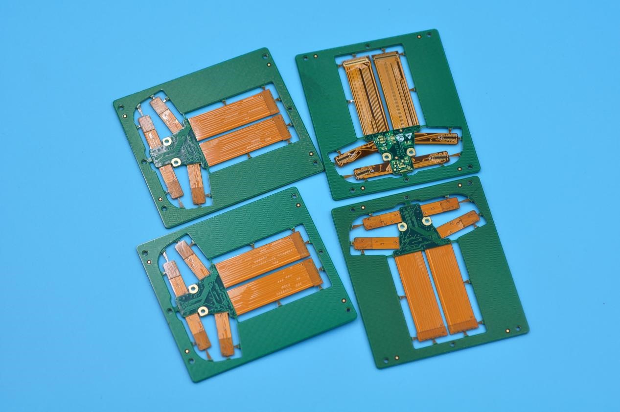
For nearly 20 years, Best Technology have always been committed to providing overseas customers High Mixed, Low Volume products with Reliable Quality and Quick Delivery, and are determined to become one of most trusted partners in the field of printed circuit boards and PCBA. As an expert of HDI PCB manufacturer, we are so confident that we can provide the highest quality product that highly meet your specifications.

hdi printed circuit board,hdi pcb manufacturer
Wednesday, August 14th, 2024

What is hdi pcb?

HDI stands for High Density Interconnect, which refers to high-density interconnect technology. HDI circuit board is a high-end printed circuit board with very high circuit density and complexity, which can achieve high-speed signal transmission and reliability design. The main features of HDI circuit board are multi-layer circuit, thin plate, small aperture, dense wiring and fine circuit. It is widely used in mobile phones, computers, network communications, automotive electronics and other fields. Bestpcb is a professional HDI manufacturer with 18 years of HDI manufacturing experience.

What are the advantages of hdi pcb

  1. Higher line density: HDI PCB can support more circuit tracks, arrange more electronic components in a limited space, and achieve high-density interconnection.
  2. Smaller device spacing: The micro-hole technology of HDI PCB allows smaller spacing between components, which is suitable for compact design.
  3. Improve signal integrity: The advanced stacking layer structure is adopted to provide better signal transmission quality and reduce signal interference.
  4. Improve reliability: The manufacturing process of HDI PCB improves the mechanical strength of the board, making it more durable and suitable for demanding application environments.
  5. Improve circuit integration: More line connections and component arrangements are achieved in a limited circuit board space to meet the needs of modern products that are thin and compact.
  6. Enhance signal transmission efficiency: The use of advanced wires and connection methods can increase the operating speed of electronic devices and reduce energy consumption.
  7. Support more complex system design: High-density connection capabilities provide support for complex system design and give full play to the performance of electronic devices. ‌
  8. Promote innovation in the electronics industry: The application of HDI technology has promoted the innovation and development of the electronics industry, making electronic equipment more intelligent and efficient. ‌
  9. Smaller size: It can complete a large number of circuit connections in a smaller space, meeting the needs of electronic products for lightness and portability. ‌
  10. Higher signal transmission speed: The high-density line design allows signals to be transmitted quickly in a short time, improving the system operation speed and response speed.

Why does HDI PCB need via filling and plating?

‌Via filling plating plays a vital role in ‌HDI PCB manufacturing, with the main purpose of improving ‌electrical performance, connection reliability, operating frequency, and avoiding electromagnetic interference. This technology fills the blind holes of HDI PCB with conductive materials through the electroplating process to form a conductive path, which improves the performance and reliability of electronic equipment.

  1. Improve electrical performance: Via filling plating can improve the electrical performance of HDI PCB, especially in high-frequency circuit board design, which is crucial for improving connection reliability, operating frequency and avoiding electromagnetic interference.
  2. Via plugging and electrical interconnection in one step: Via filling plating technology combines via plugging and electrical interconnection, avoiding the defects caused by resin via filling, and also avoiding the CTE difference caused by other materials via filling.
  3. Improve efficiency: Compared with resin via filling or other materials via filling, via filling plating has a simpler process and higher efficiency.
  4. Process flow and technical challenges of via filling plating
  5. Process flow: including steps such as tank preparation, setting of electroplating process control parameters, and analysis of potion addition.
  6. Technical challenges: including positioning accuracy issues and electroplating quality issues, which need to be solved by strictly controlling parameters such as electroplating time and current density.

Application scenarios of hole filling electroplating

First-order HDI: Suitable for electronic devices with less complex circuits.
Second-order and above blind hole electroplating copper filling: Suitable for more complex electronic devices, such as mobile phones, laptops, etc.
Comparison between hole filling electroplating and full-board electroplating
Full-board electroplating: Although it can provide a uniform surface copper thickness distribution, it may encounter the problem of residual dry film on the board surface or in the hole during pre-treatment, resulting in some areas unable to be plated with copper. In addition, the etching process after full-board electroplating may cause quality defects such as side etching and fine lines.
Hole filling electroplating: Compared with full-board electroplating, hole filling electroplating is more accurate in filling blind holes, avoiding the problems that may be encountered in full-board electroplating, while simplifying the process and improving efficiency.

Materials of HDI PCB

The materials of HDI PCB mainly include coated copper foil (RCC), prepreg, copper foil, etc.

Resin-coated copper foil (RCC): This is a material that coats a special resin film layer on electroplated copper foil, used for HDI insulation layer. The characteristics of RCC include no glass dielectric layer, easy laser and plasma micro-hole forming, extremely high peel strength and good toughness, suitable for micro-narrow line etching. Laser drilling is performed on RCC, and the aperture shape formed is an inverted trapezoid, and the general aperture size is 0.076-0.10 mm. The use of RCC makes HDI PCB more widely used in small portable products, such as mobile phones, digital cameras, laptops, etc.

Prepreg and copper foil: These are basic materials in HDI PCB manufacturing, there are no special requirements, and they are suitable for different types of HDI PCB structures. The inner layer circuits are generally 1 ounce copper thick, while the outer layer circuits are plated with half an ounce of base copper to 1 ounce of finished copper thickness. The thickness of the board is usually thinner to meet the miniaturization requirements of HDI PCB.

Other materials: In addition to the main materials mentioned above, the manufacture of HDI PCBs may also involve other materials, such as FR4, PI (polyimide), BT, etc. These materials are selected according to specific application requirements. For example, FR4 has good electrical and mechanical properties and is suitable for most general applications; PI has higher heat resistance and chemical corrosion resistance, and is suitable for high temperature, high humidity and strong acid and alkali environments, but it is more expensive and difficult to process; BT combines good electrical properties, mechanical properties and thermal stability, and is suitable for application scenarios that require higher heat resistance.

Classification of HDI circuit boards

HDI circuit boards are mainly divided into first-order, second-order, third-order, high-order (including fourth-order and above) and Anylayer HDI. ‌

  1. First-order HDI circuit boards mainly include single-sided or double-sided micro-hole processes, and the circuit layer has only one layer. ‌This type of HDI circuit board is suitable for applications with high requirements on cost and space, such as consumer electronics. ‌
  2. Second-order HDI circuit boards contain two circuit layers, which are more complex but also more powerful than first-order HDI circuit boards. They can handle higher signal frequencies and are suitable for applications that require high performance, such as high-end communication equipment and computer hardware. ‌
  3. Third-order HDI circuit boards contain three circuit layers. They are the most complex type at present. They can handle the highest signal frequency and the maximum data transmission rate. They are usually used in applications that require the highest performance, such as aerospace and military equipment. ‌
  4. High-order HDI (including fourth-order and above) The applications of third-order or fourth-order HDI in electronic terminal products are more, while those above fourth-order are mostly converted to Anylayer structure. ‌
  5. Anylayer HDI refers to HDI of any order/any layer. Compared with PCB boards with traditional lamination processes, HDI can reduce costs to a lower level when the stacking density exceeds eight layers. It also has higher electrical performance and signal accuracy, and significantly improves the performance of electromagnetic waves and radio frequency interference, electrostatic discharge and heat conduction in interconnection and relay transmission.

HDI PCB Process Flow

The process flow standards of HDI PCB mainly involve the application and processing technology of high-density interconnection technology (High Density Interconnection Technology, HDI for short), including first-order, second-order and third-order processes. Specifically, the HDI PCB process flow includes the following key steps and characteristics:

First-order process (1+N+1): This is a basic high-density interconnection technology that manufactures multi-layer boards through build-up and micro-blind via technology.

Second-order process (2+N+2): Further development on the basic technology, adding more layers and complexity.

Third-order process (3+N+3): Represents the highest stage of HDI technology, with extremely high layers and interconnection density

Differences between HDI PCB and ordinary PCBs

  1. Differences in circuit design:
    HDI PCB adopts a more sophisticated circuit design, with smaller line width and spacing, and smaller aperture, which can integrate more electronic components and realize more complex circuit functions. ‌
    The blind, buried and stacked hole designs of HDI PCB greatly improve the utilization rate and signal transmission performance of the circuit board.
  2. Differences in manufacturing process:
    The manufacturing process of HDI PCB is more complicated, requiring high-precision processes such as laser drilling technology, hole filling electroplating technology and photolithography technology.
    The manufacturing cost of HDI PCB is relatively high, but the performance and reliability are also higher. ‌
  3. Differences in application:
    Due to its high density and high performance, HDI PCB is widely used in high-end electronic products, such as smartphones, tablets, high-end communication equipment, etc.
    Ordinary PCB is mainly used in low-end electronic products and general electronic equipment.
  4. Characteristics and application scenarios of HDI PCB:
    HDI PCB has high-density wiring, multi-layer structure, high-precision manufacturing process and excellent electrical performance, which can meet the extremely high requirements of high-end electronic products for size, weight, performance and reliability.
    HDI PCB is widely used in smart phones, tablet computers, high-end communication equipment and other fields, promoting the continuous development and upgrading of electronic products.

Application of HDI PCB

HDI PCB (High Density Interconnection Printed Circuit Board) is widely used in multiple industries, including medical equipment, mobile phones, laptops, automotive electronics, computer industry, and future 5G technology fields

  1. Medical equipment: The application of HDI PCB in medical equipment, such as sphygmomanometers and ultrasonic imaging systems, achieves accurate measurement of blood pressure and high-definition imaging of the internal structure of the body, providing patients with timely and accurate diagnosis and treatment information. ‌
  2. Mobile phone industry: With the increasingly miniaturized design of mobile phones, HDI PCB is widely used in transceiver modules, motherboards, SIM card interfaces, fingerprint recognition modules and other parts of mobile phones due to its high density, high quality and high reliability. ‌
  3. Computer industry: In the computer industry, the application of HDI PCB improves the performance of computers, especially in the fields of high-speed algorithms and multimedia applications, and adapts to the miniaturization trend of computer equipment2. ‌
  4. Automotive electronics: HDI PCB has broad application prospects in the field of automotive electronics. In addition to the dominant mobile phone market, it also involves multiple fields such as automobiles, modules and artificial intelligence, demonstrating its key role in complex electronic systems. ‌
  5. Future development trends: With the advent of 5G technology, the demand for HDI PCB will continue to increase, requiring higher speeds and frequencies while adapting to smaller and thinner device designs. Research new micro HDI PCB boards to adapt to future development trends. ‌
Do You Know What Is HDI Board?
Thursday, August 10th, 2023

HDI boards are a type of printed circuit board (PCB) technology that enables higher circuit density and smaller form factors compared to traditional PCBs. HDI boards are commonly used in applications where space is limited, such as mobile devices, wearables, and aerospace systems.

Best Technology has rich experience in HDI rigid flex pcb manufacturing, below is one of our 7 layers HDI rigid flex pcb.

In Best Technology, our HDI board usually has the blind holes or buried holes, and the minimum hole size usually is 0.1mm. This board has the blind and buried holes, and the minimum hole size is 0.1mm. 100 ohm differential impedance control with 50 single ended impedance control. It’s surface finish is ENIG, 1oz copper for outer layers, 1/2oz copper for inner layers, green solder mask with white silkscreen. total thickness is 1.4mm.

Here are some key features and aspects of HDI boards:

  1. High Density: HDI boards are designed to accommodate a large number of densely packed components and interconnections. They typically have multiple layers with high routing density, allowing for more complex circuitry in a smaller footprint.
  • Microvias: HDI boards extensively use microvias, which are very small holes drilled into the board to create electrical connections between different layers. Microvias are smaller in size compared to traditional vias, allowing for increased routing density.
  • Staggered and Stacked Microvias: HDI boards employ different types of microvias, including staggered and stacked microvias. Staggered microvias connect adjacent layers, while stacked microvias connect non-adjacent layers, providing even higher routing density.

Blind and Buried Vias: HDI boards often utilize blind and buried vias, which are vias that do not extend through the entire board. Blind vias connect an outer layer with one or more inner layers, while buried vias connect inner layers only. These vias help optimize space and increase routing capabilities.

  • Fine Pitch Components: HDI boards support the use of fine pitch components, such as microcontrollers, ball grid array (BGA) packages, and small surface-mount devices (SMDs). The high routing density and smaller features of HDI boards make them suitable for accommodating these tiny components.
  • Increased Signal Integrity: HDI boards can provide improved signal integrity due to shorter trace lengths and reduced noise interference. The compact design minimizes signal loss and impedance mismatches, allowing for better performance in high-frequency applications.
  • Design Considerations: Designing HDI boards requires expertise in factors such as layer stacking, via types, trace widths, and clearances. Advanced design software and manufacturing techniques are often employed to ensure precise alignment and reliability of the intricate interconnections.
  • Manufacturing Challenges: HDI boards can be more challenging to manufacture compared to standard PCBs. The use of smaller features and complex layer structures requires specialized fabrication techniques, such as laser drilling, sequential lamination, and precise registration control.

HDI technology has become increasingly prevalent in the electronics industry, enabling the development of smaller, lighter, and more sophisticated devices. It offers enhanced electrical performance, improved reliability, and greater design flexibility. If you have any comments about the HDI board, please feel free to contact Best Technology Team e-mail: sales@bestfpc.com.

Do You Ever Know High Density Interconnect PCBs?
Tuesday, December 31st, 2019

HDI PCB (High Density Interconnector PCB), is a printed circuit board having a relatively high line distribution density using the micro-blind and buried hole technology.

It is a process that includes an inner layer line and an outer layer line, then uses a hole and a metallization in the hole to realize a joint function between the inner layers of each layer.

HDI PCB-1
HDI PCB-1

With the development of high-density, high-precision electronic products, the requirements of high-density and high precision are imposed on printed circuit boards. The most effective way to increase the density of pcb is to reduce the number of through holes, and to accurately set the blind holes and buried holes to achieve this requirement, thereby an HDI PCB came into being.

HDI PCBs are finding their way into a growing number of products:

Military communications devices and other strategic equipment

Aerospace – smaller space requirements and light weight are ideal for such applications

Computers and smartphones – phones and computers are taking full advantage of smaller profiles, reduced weight, and increased functionality, made possible through the integration of HDI circuits.

HDI PCB-2
HDI PCB-2

Medical equipment – diagnostic and monitoring equipment has become more reliable and expanded with technical features that aid medical teams with patient treatment, and all of this is powered by HDI PCBs and advanced software.

Benefits of HDI PCB

HDI PCB utilizes buried or blind vias, or a combination, and may also incorporate microvias with an incredibly small diameter. This facilitates the incorporation of more technology in less space, with fewer layers. Multi-layer HDI PCB are also in common use, with many layers being accommodated through various construction methods utilizing blind, buried, stacked, and staggered vias.

With smaller components and blind via in pad technology, components may be placed closer together, resulting in faster signal transmission rates while also reducing crossing delays and signal loss. These are key considerations that generate improved performance of HDI PCBs.

HDI PCBs are preferred for applications where space, performance, reliability, and weight are concerns. This makes them more suitable for nearly every application related to electronics, consumer products, computers, and aeronautics.

Multi-layer HDI PCB can provide strong interconnection of stacked vias, resulting in high levels of reliability, even in more extreme environments.

Considering this, do you ever think about choosing HDI PCB on your next project?