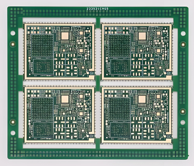
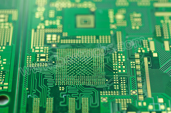
High Density Interconnect PCB refers to a multilayer structure that uses laser microvias, thin dielectric layers, and sequential lamination to increase routing density and improve electrical performance. Instead of routing signals through long mechanical vias, HDI stackup design focuses on short vertical transitions between adjacent layers. This reduces inductance, improves impedance control, and allows fine-pitch BGA escape without increasing board size.
Typical HDI electrical parameters used in engineering documentation include:
Line width / spacing: 60–75 µm (advanced builds may reach 40 µm)
HDI stackup design emphasizes signal-reference plane proximity. Short dielectric spacing lowers loop inductance and stabilizes return paths, which becomes critical in AI server and high-speed computing boards.
High Density Interconnect PCB
When Should You Choose an HDI PCB Instead of a Standard Multilayer PCB for AI Server or High-Speed Systems?
HDI becomes necessary when routing density or electrical requirements exceed conventional PCB capability. AI server motherboards, accelerator modules, and edge computing boards frequently adopt HDI because processor pin counts and high-speed channels increase dramatically.
Engineering decision indicators:
BGA pitch ≤ 0.5 mm
High-speed links above 10–25 Gbps
Large processor or FPGA packages exceeding 1000 pins
Board size constraints requiring compact layouts
Power delivery networks needing dense decoupling arrays
In AI server designs, HDI reduces via stubs and shortens differential pair transitions. This helps maintain insertion loss budgets and improves eye-diagram margins during high-frequency operation.
How Do 1+N+1 and 2+N+2 HDI Stackup Design Strategies Affect Routing Density and Manufacturing Risk?
More build-up layers increase routing flexibility but also introduce additional lamination cycles. Engineers often begin with 1+N+1 and evaluate whether further build-up layers are required based on BGA escape results.
HDI Microvia Engineering Parameter Table
Parameter
Recommended Range
Engineering Impact
Laser Via Diameter
75–100 µm
Routing density and plating reliability
Capture Pad Size
150–250 µm
Annular ring control
Aspect Ratio
≤ 0.8:1
Prevents plating voids
Via Structure
Staggered preferred
Improves thermal reliability
Copper Fill Thickness
15–25 µm cap
Required for via-in-pad
Microvia planning should begin during stackup definition because changing via structure later can require redesigning large portions of the layout.
When Does Via-in-Pad Become Mandatory in Fine-Pitch HDI PCB and AI Server BGA Fanout?
Via-in-pad is used when routing channels around BGA pads are insufficient. In AI server processors or high-density networking ASICs, pad pitch often forces vertical signal escape.
Dense decoupling networks under core voltage rails
VIP pads require copper filled microvias, planarization to maintain flatness, and careful solder mask design.
How Does HDI PCB Compare to Standard PCB in Signal Integrity, Size Reduction, and Layer Utilization?
Engineering Metric
HDI PCB
Standard PCB
Via Stub Length
Very Short
Long unless backdrilled
Routing Channel Density
High
Limited
Loop Inductance
Lower
Higher
Board Area
Reduced
Larger
Layer Efficiency
High utilization
Lower utilization
EMI Performance
Improved due to compact loops
Depends on layout strategy
Shorter vertical transitions in HDI improve signal eye margin in high-frequency environments such as AI servers.
What Is the Real HDI Fabrication Flow and Which Process Steps Affect Yield Most?
HDI Fabrication Process Table
Step
Key Parameter Control
Risk Area
Core Lamination
Thickness tolerance ±10 µm
Warpage
Build-Up Lamination
Resin flow uniformity
Void formation
Laser Drilling
Position accuracy ±20 µm
Via misalignment
Copper Plating
Current density control
Microvia reliability
Imaging & Etch
Line width tolerance ±10 µm
Signal impedance shift
Microvia plating uniformity and dielectric thickness control are major contributors to HDI manufacturing yield.
Which Materials Are Preferred for HDI Stackup Design in AI Server PCB and High-Speed Applications?
Material Category
Dk Range
Df Range
Typical Use
High Tg FR-4
3.8–4.2
0.015–0.018
General HDI boards
Low Loss Laminate
3.2–3.6
0.004–0.009
AI server and networking
RCC Thin Dielectric
~3.5
0.01
Build-up layers
Material selection should align with both electrical performance targets and thermal cycling conditions during assembly.
How Do Engineers Route Fine-Pitch BGA on HDI PCB Without Signal Integrity Problems or Rework Risk?
Routing strategy begins with stackup planning rather than trace drawing. Engineers typically follow a structured workflow:
Assign ground reference layers adjacent to signal layers
Escape first BGA rows using microvias to inner routing layers
Maintain differential pair spacing within controlled tolerance
Avoid excessive layer transitions that introduce impedance discontinuities
Typical HDI differential routing parameters used in AI server layouts:
Pair spacing: 100–150 µm
Trace width: 65–80 µm
Reference plane spacing: 60 µm
How Can You Improve HDI PCB Reliability Against CAF, Microvia Fatigue, and Warpage?
Failure Mechanism
Root Cause
Engineering Control
CAF Growth
Moisture + voltage bias
Increase conductor spacing
Microvia Fatigue
CTE mismatch
Use staggered microvias
Warpage
Copper imbalance
Symmetrical copper distribution
Balanced copper distribution across layers significantly improves long-term reliability in high-power computing environments.
What Drives HDI PCB Cost and How Does a Detailed HDI Cost Breakdown Help Engineering Decisions?
HDI Cost Breakdown Engineering Table
Cost Driver
Process Impact
Cost Influence
Sequential Lamination
Additional build-up layers
High
Laser Microvia Drilling
Equipment time
Medium-High
Copper Filled VIP
Extra plating steps
Medium
Fine Line Imaging
Tight tolerance control
Medium
Low Loss Material
Material premium
Variable
Understanding HDI cost breakdown allows engineers to optimize stackup design early and avoid unnecessary process steps.
Why Choose EBest as Your High Density Interconnect PCB Manufacturer?
If you are moving into HDI PCB projects, your biggest risk is not the CAD work. It is misalignment between design intent and fabrication reality. EBest Circuit positions itself as a one-stop PCBA service provider that better understands the needs of engineers, so your stackup, microvias, and assembly choices stay consistent from quote to shipment.
Free DFM and process adaptation suggestions before release
20 years serving 1800+ customers and 10,000+ engineers
One-Stop Service: PCB, components, PCBA, testing, and box-building
No MOQ with personal service for prototypes and small batches
ISO9001/ISO13485, IATF16949, AS9100D quality systems support
MES & traceability for process tracking and accountability
1.5-week rapid PCBA delivery options for urgent programs
Technical support before and after sales, with prompt feedback (often within 12 hours)
Prototype & small volume welcome, with quick turn-out and on-time delivery focus
High quality builds, special requests available, supported by a strong R&D team
FAQs
1. What BGA pitch usually requires HDI stackup design?
HDI stackup design is commonly selected when BGA pitch approaches 0.5 mm because routing density becomes constrained using only mechanical vias.
2. Is 2+N+2 always required for AI server HDI PCB?
Many AI server boards begin with 1+N+1 structures and only move to 2+N+2 when routing density requires additional build-up layers.
3. Are stacked microvias reliable for high-power systems?
Stacked microvias can be reliable when copper filling and plating thickness are well controlled, though staggered structures often improve durability.
4. Does HDI PCB always reduce total layer count?
HDI improves routing efficiency and signal integrity but does not always reduce total layer count.
5. How early should HDI stackup design be finalized?
Stackup definition should occur before placement and routing to prevent redesign cycles.
HDI printed circuit boards are advanced multilayer boards that utilize high-density interconnect technology to accommodate more components in a smaller area, enabling the miniaturization and enhanced performance of modern electronics. This comprehensive guide will explore the intricacies of HDI PCB technology, its manufacturing process, and the critical importance of choosing a partner with full turnkey capability for your project’s success.
Navigating the complex world of advanced PCB procurement can be fraught with challenges. Are you struggling to balance high performance with tight project constraints? Common pain points include:
Managing Sky-High Complexity: HDI designs with microvias and multiple lamination cycles introduce significant manufacturing and design validation hurdles.
Controlling Unpredictable Costs: Quotes that spiral due to unforeseen process steps, material waste, or yield issues with delicate HDI structures.
Suffering from Fragmented Supply Chains: Coordinating separately with design houses, board fabricators, and assembly shops leads to communication gaps, finger-pointing, and delayed timelines.
Ensuring Reliable Performance: Anxiety over signal integrity in dense layouts and the long-term reliability of microvias under thermal and mechanical stress.
Navigating Opaque Vendor Capabilities: Difficulty verifying if a supplier truly has the specialized equipment and expertise for your specific HDI level and technology needs.
The most effective path to mitigating these risks is partnering with a manufacturer that offers genuine full turnkey capability. This means:
Integrated Design Support: Expert HDI PCB design guidance from the start to prevent costly manufacturability issues.
Transparent Cost Engineering: Clear cost breakdowns and design-for-manufacturing (DFM) advice to optimize the HDI printed circuit boards price.
Seamless Process Ownership: A single point of accountability managing the entire flow from Gerber files to tested assemblies.
Advanced Process Validation: Rigorous testing protocols, including cross-sectioning and thermal cycling, for reliability assessment of microvias in HDI printed circuit boards.
Demonstrable Technical Expertise: Clear evidence of in-house advanced equipment and a proven track record with complex HDI builds.
At BEST Technology, we specialize in transforming these complex challenges into seamless solutions. As a professional HDI PCB manufacturer with robust full turnkey services, we own and manage the entire process—from design review and prototyping to sophisticated fabrication, precise assembly, and rigorous testing. Our expertise ensures your high-density interconnect projects are not only manufacturable but also optimized for performance, cost, and reliability. For your next project, pls feel free to contact our experts at sales@bestpcbs.com.
What are HDI Printed Circuit Boards?
HDI printed circuit boards are advanced PCBs designed for high wiring density and compact electronic systems. They rely on microvia technology, fine-line routing, and multilayer stackups to support complex interconnections within limited board space.
Key characteristics of HDI printed circuit boards include:
High wiring density Enables more signal routing and component placement in smaller board areas.
Microvia technology Uses laser-drilled blind and buried vias, typically ≤ 0.15 mm in diameter, to replace traditional mechanical through-holes.
Fine line width and spacing Supports ultra-fine traces and tight spacing for high-density component layouts.
Advanced multilayer stackups Incorporates sequential lamination and any-layer interconnect structures for greater design flexibility.
Improved signal integrity Shorter interconnect paths and optional low-Dk/Df materials help maintain performance in high-speed designs.
Specialized manufacturing processes Requires precision laser drilling, controlled lamination, and strict process control during the HDI PCB manufacturing process.
In summary, HDI printed circuit boards are not simply denser versions of standard PCBs. They represent a dedicated design and manufacturing approach that enables modern, high-performance electronic products with strict size and performance constraints.
What Makes HDI Circuit Boards Different From Standard Multilayer PCBs?
While both are multilayer structures, HDI PCBs are fundamentally different in their construction and capabilities. Standard multilayer PCBs use mechanical drilling for through-hole vias, which limits density. HDI circuit boards, however, are defined by their use of microvias (typically with a diameter of less than 150µm), which allow for direct interconnections between adjacent layers, unlocking new routing possibilities.
Feature
Standard Multilayer PCB
HDI PCB
Via Technology
Primarily through-hole vias
Microvias, blind/buried vias
Line Width/Space
Larger (e.g., ≥ 4 mil)
Finer (e.g., ≤ 3 mil)
Pad Density
Lower
Much Higher
Construction
Fewer lamination cycles
Multiple sequential laminations
Key Benefit
Cost-effective for simpler designs
Enables miniaturization & high-speed performance
The distinction lies in the high density interconnect approach, which provides superior electrical performance and design freedom, making it ideal for complex, space-constrained applications.
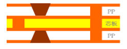
What Is the Structure of HDI Printed Circuit Boards?
The structure of HDI printed circuit boards is not defined by a single, fixed stackup or manufacturing flow. Instead, HDI construction is highly flexible and is determined primarily by via requirements, drilling methods, and interconnection density. The layer structure and production sequence are customized to meet specific routing and component layout demands.
At the core of HDI PCB structure is the combination of multiple via types, each serving a different interconnection purpose:
Laser-drilled blind vias These microvias connect an outer layer to one or more adjacent inner layers. They are a defining feature of HDI printed circuit boards and enable high routing density while minimizing signal path length.
Mechanically drilled buried vias Buried vias connect inner layers without reaching the outer surfaces. They support complex multilayer interconnections and help free surface area for fine-pitch components.
Mechanically drilled through holes Through holes extend from the top layer to the bottom layer and are typically used for power distribution, grounding, or components that require mechanical strength.
Because HDI printed circuit boards often rely on sequential lamination, the final structure may include multiple build-up layers, stacked or staggered microvias, and hybrid via combinations. As a result, each HDI design follows a drilling-driven structural logic, rather than a standardized process template.
In practice, the structure of HDI printed circuit boards is engineered around via architecture, layer interconnect strategy, and manufacturing feasibility, allowing designers to balance density, reliability, and performance in advanced electronic systems.
What Are the Blind Via Types in HDI Printed Circuit Boards?
In HDI printed circuit boards, blind vias are created primarily by laser drilling and are used to connect surface layers to inner layers without penetrating the entire board. Different blind via structures are selected based on layer count, routing density, and reliability requirements.
Common blind via types used in HDI printed circuit boards include:
Microvia hole Typically used in 1+N+1 HDI structures, microvias connect the outer layer to the adjacent inner layer. These vias are laser-drilled and are not copper-filled, making them suitable for simpler HDI designs with moderate density requirements.
Solid via hole (filled microvia) Also applied in 1+N+1 structures, solid vias are laser-drilled microvias that require copper filling. The filled structure provides a flat surface for component pads and supports higher reliability and finer pitch components.
Staggered via hole Used in second-order HDI, staggered vias consist of offset laser-drilled microvias on different layers. This structure reduces stress concentration and is commonly chosen for improved reliability in multilayer HDI designs.
Stacked via hole A key feature of high-density and any-layer HDI, stacked vias are vertically aligned laser-drilled microvias. These vias must be copper-filled to ensure mechanical strength and electrical continuity across multiple layers.
Skip via hole Skip vias are laser-drilled microvias that connect non-adjacent layers, such as from layer 1 directly to layer 3, bypassing layer 2. This structure increases routing flexibility while maintaining surface density.
Step via hole Step vias are co-located second-order laser vias that are not copper-filled. They are typically used in designs where surface planarity is less critical but routing density must still be increased.
How to distinguish blind via structures in HDI designs:
Whether the design is 1+N+1 This indicates the most basic HDI build-up structure, where laser-drilled blind vias connect the outer layers to the adjacent inner layers.
Whether the design is second-order HDI Second-order HDI involves connecting to deeper layers using two sequential microvias, typically requiring either staggered or stacked via structures.
Staggered vs. stacked vias The key distinction is whether the two microvias are vertically aligned.
Staggered vias are offset between layers.
Stacked vias are directly aligned on the same vertical axis.
Filled vs. non-filled vias
Designs using via-in-pad, requiring high surface planarity or higher long-term reliability, typically require copper-filled vias.
Vias that are not located in pads and are used in cost-sensitive designs may remain unfilled, depending on reliability requirements and manufacturing capability.
Each blind via type in HDI printed circuit boards serves a specific structural and electrical function. The selection depends on factors such as layer stackup, component pitch, signal integrity requirements, and manufacturing capability, making blind via design a critical part of HDI PCB engineering.
What Equipment Do HDI Printed Circuit Boards Factories Use for Microvias?
UV or CO₂ Laser Drilling Machines: For ablating precise, small-diameter microvias (as small as 50µm).
Advanced Direct Imaging (DI) Systems: To expose ultra-fine line traces and spaces with high accuracy.
Fully Automated Optical Inspection (AOI): To detect minute defects in traces, spaces, and via pads.
Electroless and Electrolytic Copper Plating Lines: For uniform copper deposition into high-aspect-ratio microvias.
Sequential Lamination Presses: To build the multilayer structure with precise layer-to-layer registration. This specialized toolset is non-negotiable for achieving the yields and quality required in the competitive HDI printed circuit board market.
How to Identify HDI Levels in HDI Printed Circuit Boards?
Identifying the HDI level of HDI printed circuit boards primarily depends on the via structure, rather than on trace etching or basic layer count. While routing processes for multilayer PCBs are largely similar to those used for single- or double-layer boards, the defining difference lies in how vias are formed and interconnected.
At a high level, PCB constructions can be classified into through-hole boards, first-order HDI, second-order HDI, and stacked HDI. Higher-order and any-layer HDI structures exist, but they are used far less frequently due to significantly higher cost and manufacturing complexity.
Through-Hole Boards (Non-HDI)
Through-hole boards use a single via type that runs from the top layer to the bottom layer. All interconnections—both outer and inner—are completed using mechanically drilled through holes that are subsequently copper plated.
The number of layers does not determine whether a board is HDI. A 2-layer PCB is typically a through-hole board, but many high-end products such as network switches or military electronics use 20-layer boards that are still entirely through-hole. Typical finished via diameters range from 0.2 mm to 0.3 mm, with smaller diameters increasing cost due to drill wear and slower drilling speeds.
First-Order HDI (1st-Order HDI)
A first-order HDI board is identified by the presence of one layer of laser-drilled microvias on each outer surface. These microvias usually have diameters around 0.1 mm and connect the outer layers to the adjacent inner layers.
Structurally, a common example is a 6-layer first-order HDI board, which can be viewed as a 4-layer through-hole core with one HDI build-up layer added to each side. The inner layers still rely on mechanical vias, while the outer layers use laser microvias.
Laser drilling only penetrates dielectric material and does not cut through copper, allowing precise via formation without damaging internal circuitry.
Second-Order HDI (2nd-Order HDI)
A second-order HDI board contains two layers of laser-drilled microvias on each side of the core. In practical applications, second-order HDI structures are most commonly found in 8-layer or higher designs, rather than in 6-layer boards.
There are two main second-order configurations:
Staggered vias The two layers of laser microvias are offset from each other. This approach is used because unfilled microvias cannot reliably support another laser via drilled directly on top. Staggered structures reduce process risk and are more cost-effective.
Stacked vias In stacked structures, the laser microvias are vertically aligned. To make this reliable, the lower microvia must be copper-filled before drilling the upper microvia. This process is more complex and significantly more expensive but enables tighter routing density.
In terms of structure:
A 6-layer second-order HDI board can be viewed as a 4-layer first-order board with an additional HDI build-up.
An 8-layer second-order HDI board is effectively a 6-layer first-order board with another build-up layer added.
Any-Layer HDI
Any-layer HDI represents the highest level of HDI technology. Every layer is interconnected using laser-drilled microvias, and any layer can connect directly to any other layer.
This structure offers maximum routing freedom and density, making layout significantly easier for engineers. However, the cost is extremely high—often more than ten times that of a standard through-hole board—so any-layer HDI is reserved for only the most compact and performance-critical designs.
In practice, HDI levels in HDI printed circuit boards are identified by answering three key questions:
Are laser-drilled microvias present? If not, the board is a through-hole design.
How many layers of microvias are used? One layer indicates first-order HDI; two layers indicate second-order HDI.
Are the microvias staggered or stacked? Staggered vias suggest cost-optimized second-order HDI, while stacked vias indicate higher-density, higher-cost designs.
By examining via type, drilling method, and build-up layer count, the HDI level of a printed circuit board can be accurately determined, independent of total layer count alone.
How Does HDI Technology in PCB Improve Signal Integrity?
HDI technology in PCB is a cornerstone for high-speed digital and RF applications because it inherently enhances signal integrity (SI).
Shorter Interconnect Paths: Microvias enable more direct routing, reducing signal path length and propagation delay.
Reduced Parasitics: Smaller via stubs and pads lower parasitic inductance (L) and capacitance (C), minimizing unwanted signal reflection and attenuation.
Better Impedance Control: Finer lines and consistent dielectric layers allow for more precise control over characteristic impedance.
Improved Power Integrity: Dense via-in-pad technology provides low-inductance paths for power delivery networks (PDNs), reducing switching noise.
Enhanced EMI/EMC Performance: Tighter component placement and optimized grounding via microvias help contain electromagnetic interference. These SI benefits make HDI printed circuit boards essential for 5G, high-performance computing, and advanced automotive electronics.
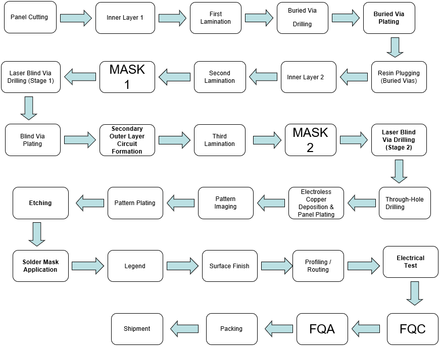
HDI PCB Manufacturing Process Explained Step by Step
In HDI production, the “step-by-step” flow changes with the stackup and via strategy.
Example 1: 1+4+1 (B) Process Flow
(Two lamination cycles, with inner mechanical drilling and plating performed before the second lamination, then laser microvias after the second lamination.)
Panel Cutting
Inner Layer Imaging & Etching
1st Lamination (First Press)
L2–L5 Mechanical Drilling
L2–L5 Copper Plating
L2–L5 Inner/Outer Layer Circuit Formation (for the sub-structure)
2nd Lamination (Second Press)
Laser Drilling (Microvias)
Mechanical Drilling (Through Holes / Tooling Holes as required)
Copper Plating (Via Metallization)
Outer Layer Imaging & Etching
Solder Mask Application
ENIG (Electroless Nickel Immersion Gold)
Legend / Silkscreen Printing
Profiling / Routing (Final Outline)
Electrical Test (E-test)
Final Inspection
OQC (Outgoing Quality Control)
Packing
Warehouse Receiving (Stock-in)
Example 2: 1+4+1 (A) Process Flow
(Single lamination cycle, then laser drilling and standard downstream flow.)
Panel Cutting
Inner Layer Imaging & Etching
Lamination (Pressing)
Laser Drilling (Microvias)
Mechanical Drilling (Through Holes / Tooling Holes as required)
Copper Plating (Via Metallization)
Outer Layer Imaging & Etching
Solder Mask Application
ENIG (Electroless Nickel Immersion Gold)
Legend / Silkscreen Printing
Profiling / Routing (Final Outline)
Electrical Test (E-test)
Final Inspection
OQC (Outgoing Quality Control)
Packing
Warehouse Receiving (Stock-in)
The practical difference between 1+4+1 (A) and 1+4+1 (B) is whether the build requires a staged sequence with an early drill-and-plate step before the second lamination. That staged approach adds process control points and complexity, which often affects lead time and cost.
Example 3: 1+1+8+1+1 Process Flow
Using a 12-layer, double-lamination first-order HDI structure (1+1+8+1+1) as an example, the following briefly outlines the standard manufacturing process commonly used in the industry.
What Applications Use HDI Circuit Boards Most Frequently?
HDI circuit boards are most widely used in applications that demand high signal density, compact form factors, and reliable high-speed performance. As electronic systems continue to evolve toward higher integration and smaller footprints, HDI technology has become a foundational solution across several major industries.
Consumer Electronics and Smartphones
Smartphones remain the largest application segment for HDI circuit boards, accounting for more than half of total HDI demand. Modern smartphone mainboards rely heavily on HDI structures to support high pin-count processors, dense memory interfaces, and multi-antenna RF layouts within extremely limited space.
HDI enables fine line routing, multi-layer interconnects, and compact board stacking, making it essential for slim device profiles and advanced functionality. Wearable electronics further extend this demand, using HDI and embedded via technologies to significantly reduce PCB area.
PC, Consumer Computing, and High-Performance Devices
PCs, tablets, and other consumer computing products represent a rapidly expanding HDI application area. As processors become more powerful and interfaces move toward higher speeds, HDI circuit boards are increasingly adopted to meet routing density and signal integrity requirements.
This segment has grown to roughly one-third of overall HDI demand, driven by compact laptops, high-performance computing modules, and emerging AI-enabled consumer devices.
Automotive Electronics and ADAS Systems
Automotive electronics, particularly ADAS and intelligent vehicle platforms, are a fast-growing HDI application. Vehicle systems require HDI circuit boards to support synchronized multi-sensor signal processing, high-speed data transmission, and stable operation under thermal stress and vibration.
HDI technology enables reliable high-density interconnects for camera modules, radar systems, and in-vehicle infotainment, making it a critical component in the transition toward autonomous and intelligent vehicles.
Communication Infrastructure and 5G Equipment
HDI circuit boards are widely used in 5G base stations and communication equipment, where high-frequency, low-loss signal transmission is essential. These systems require fine-line HDI layouts to support large antenna arrays, RF front-end integration, and high-speed signal processing.
The increasing complexity of 5G infrastructure continues to push higher layer counts and tighter precision requirements, accelerating HDI adoption in telecom applications.
Medical Electronics and Healthcare Devices
Medical electronics represent a smaller but high-value HDI segment. Advanced imaging systems, implantable medical devices, and portable diagnostic equipment rely on HDI circuit boards to achieve miniaturization, high reliability, and precise signal acquisition.
HDI flexible and rigid-flex structures are particularly important in medical applications where space constraints and signal accuracy are critical.
AI Servers and Emerging High-Growth Segments
AI servers and data-center hardware are emerging as one of the fastest-growing HDI application areas. The need for ultra-high interconnect density, high-speed signal integrity, and multilayer routing has made HDI circuit boards a key enabler for advanced computing platforms.
As AI workloads and server architectures continue to evolve, higher-order HDI and any-layer HDI solutions are increasingly replacing traditional PCB designs.
In summary, HDI circuit boards are most frequently used in:
Smartphones and consumer electronics
PCs, tablets, and high-performance consumer devices
Automotive electronics and ADAS systems
5G communication infrastructure
Medical and healthcare electronics
AI servers and advanced computing hardware
Across these applications, HDI technology plays a central role in enabling miniaturization, high-speed performance, and system-level integration, making it one of the most important PCB technologies in modern electronics manufacturing.
What Capabilities Should You Expect From an HDI PCB Manufacturer?
When selecting an HDI PCB manufacturer, particularly one claiming full turnkey capability, it’s crucial to understand the specific advanced technological competencies they must possess. A true specialist in high density interconnect must demonstrate proficiency far beyond standard PCB fabrication. Based on our internal process capabilities at BEST Technology, here are the definitive capabilities you should expect from a leading HDI PCB manufacturer.
An advanced HDI printed circuit board supplier must be able to deliver on the following key areas to ensure your HDI printed circuit boards meet the highest standards of performance, miniaturization, and reliability:
Laser Drilling Mastery: The capability to consistently drill microvias with diameters down to 0.070mm (limit) or 0.10mm (standard), a fundamental requirement for what is HDI PCB. This includes controlling the depth-to-diameter ratio precisely.
Complex Lamination Expertise: Proficiency in executing multi-stage sequential lamination processes (1+N+1, 2+N+2, etc.) with exceptional layer-to-layer registration (alignment tolerance ≤0.13mm standard, ≤0.10mm limit). This is critical for building reliable any-layer HDI printed circuit boards.
Ultra-Fine Line & Space Imaging:
Sub-4mil Resolution: The ability to reliably manufacture extremely fine traces and spaces. For outer layers, this means achieving 3.5/4mil (standard) or even 3/3mil (limit). On inner layers, capabilities extend to 3/3mil (standard) or 2.5/2.5mil (limit), which is essential for high density PCB designs requiring maximum component density.
Controlled Etching: Maintaining tight etch tolerances (e.g., ±1mil for lines ≤5mil) to ensure geometric accuracy and consistency.
Advanced Impedance Control:
Dielectric Management: Precise control over insulation layer thickness (minimum 0.076mm standard) and material properties to achieve consistent electrical characteristics.
Targeted Impedance Performance: Delivering specified impedance values (e.g., 50Ω, 100Ω differential) with tight tolerances (±5Ω for <50Ω impedance, standard), which is vital for maintaining signal integrity in high-speed HDI technology in PCB applications.
Broad Material & Surface Finish Portfolio:
High-Performance Substrates: Access to and proven experience with a wide variety of materials, including standard FR4 (normal, medium, and high TG), high CTI materials, and specialized high-frequency/low-loss laminates (e.g., Rogers, Taconic series), catering to demanding applications in the HDI printed circuit board market.
Diverse Surface Treatments: Offering a comprehensive range of surface finishes such as ENIG, Immersion Tin/Silver, OSP, Hard/Soft Gold, and ENEPIG to meet various assembly requirements and component specifications.
Integrated Full-Turnkey Services:
Proactive Design Support (DFM): Providing expert engineering feedback during the design phase to optimize for manufacturability, performance, and HDI printed circuit boards price considerations.
Seamless Fabrication-to-Assembly Flow: Managing the entire process under one roof, from HDI PCB manufacturing process execution to precision SMT/BGA assembly, ensuring quality, traceability, and faster time-to-market.
Rigorous Testing & Validation: Implementing thorough testing protocols, including electrical testing (flying probe, ICT), AOI, and functional testing, to guarantee the reliability of complex HDI assemblies.
In summary, a premier HDI printed circuit board supplier with full turnkey capability integrates these sophisticated technologies and services. BEST Technology’s detailed process capabilities, as reflected in our manufacturing specifications, underscore our commitment to delivering the highest quality HDI printed circuit boards for the most challenging applications. We possess the advanced infrastructure, technical expertise, and integrated services necessary to transform your complex HDI designs into successful, high-performance products.
How to Choose a Reliable HDI Printed Circuit Board Supplier?
Choosing the right HDI printed circuit board supplier is a strategic decision. Follow this checklist:
Audit Technical Certifications: Look for ISO 9001, IATF 16949 (automotive), and relevant industry-specific certifications.
Review Their Portfolio: Examine case studies or samples of similar complexity (HDI level, layer count, material).
Evaluate Communication: Assess their responsiveness, engineering support, and willingness to provide HDI printed circuit boards quotes with clear breakdowns.
Request a Facility Tour/Virtual Audit: Verify their equipment (laser drillers, DI machines) and process controls.
Check Supply Chain Stability: Ensure they have strong relationships with material suppliers to mitigate shortage risks.
Discuss Prototype & Volume Scalability: Confirm they can support both rapid prototyping and volume production. Thorough vetting separates true technical partners from basic board vendors.
HDI Printed Circuit Boards Price Factors and Cost Considerations
The HDI printed circuit boards price is influenced by multiple, often interrelated, factors. Understanding them helps in budget planning and design optimization.
Layer Count & Board Size: More layers and custom sizes use more material and process time.
Material Type: Standard FR-4 vs. high-speed/low-loss or halogen-free materials.
Minimum Feature Size: Tighter trace/space and smaller microvia diameters require more precise (and expensive) processes.
Surface Finish: ENIG, ENEPIG, or hard gold are costlier than HASL.
Quantity & Lead Time: Prototype quantities have higher unit costs; expedited turnarounds incur premiums. A trusted manufacturer will work with you to find the most cost-effective design path without compromising critical performance.
How Is the HDI Printed Circuit Board Market Evolving With AI and 5G?
The HDI printed circuit board market is undergoing a fundamental transformation, shifting from a cycle driven primarily by consumer electronics miniaturization to one powered by the high-performance demands of artificial intelligence (AI) and ubiquitous 5G connectivity. This evolution is not merely a growth in volume but a strategic upgrade in technology, value, and application focus, creating new high-growth segments and reshaping competitive dynamics.
1. Market Overview: From 5G Build-out to an AI-Powered Future
The market trajectory clearly illustrates this shift. In 2023, the global HDI board market, valued at approximately 8.5 billion with China accounting for4210 billion, growing at a rate of 9.2%, primarily fueled by AI servers and automotive electronics. This is moving the industry’s focus from volume to advanced capability, as seen in the rising proportion of Any-layer HDI, projected to reach 28% by 2025.
2. Primary Growth Drivers: A Confluence of Megatrends
The demand surge is coming from multiple, synergistic frontiers:
AI Server Demand Explosion: This is the most potent driver. AI training chips (e.g., NVIDIA H100) require HDI boards with 20+ layers, with per-unit value reaching 3-5 times that of traditional servers. The global market for HDI in AI servers is forecast to surpass $2.5 billion by 2025. This creates intense demand for boards that support heterogeneous integration technologies like 2.5D/3D packaging and can manage thermal loads from chips consuming over 1000W.
Automotive Electronics Penetration: Advanced Driver-Assistance Systems (ADAS) and smart cockpits are drastically increasing HDI content per vehicle from 1-2 pieces to 5-8 pieces. The automotive segment’s share of the HDI market is expected to rise from 15% to 25% by 2025, demanding ultra-high reliability.
Accelerated 5G & Data Center Infrastructure: The rollout of Massive MIMO antennas and the upgrade to 800G optical modules in data centers require high-frequency, high-speed HDI boards with extremely fine line widths/spaces (below 20µm) and ultra-low signal loss, pushing the limits of manufacturing processes like mSAP.
3. Application Shift: Beyond the Smartphone Core
While smartphones remain the dominant application, accounting for 58% of demand, the future growth engine is demonstrably elsewhere. The combined share of PC/consumer electronics (30%) and automotive electronics (7%) highlights HDI’s expanding role in computing and automotive intelligence. The 42% non-smartphone segment represents a vast technology substitution space, where high-end HDI is progressively replacing traditional PCBs, a process that will continue to deepen.
4. Technological and Supply Chain Transformation
The requirements of AI and 5G are forcing a comprehensive upgrade across the HDI PCB manufacturing ecosystem:
Technology Trends: Line/space is advancing toward 30/30µm, and the penetration of SLP (Substrate-Like PCB) technology is increasing.
New Capabilities Required: Manufacturers must master advanced thermal management (embedded copper blocks, metal cores), supply ultra-low-loss materials for high-frequency applications, and build full turnkey capabilities—from collaborative design and simulation to full-scale production and testing—to meet the stringent demands of clients like NVIDIA.
In summary, the HDI printed circuit board market is decisively evolving from enabling device miniaturization to becoming the critical backbone of the AI and 5G infrastructure. Growth is being driven by high-value, high-complexity applications in AI servers, autonomous vehicles, and advanced communications, which in turn are triggering a wave of technological innovation and supply chain restructuring. Manufacturers that can master advanced processes like Any-layer HDI, ultra-fine line imaging, and integrated thermal management, while providing comprehensive full turnkey solutions, are positioned to lead the next phase of the industry’s evolution.
In conclusion, HDI printed circuit boards are the foundational technology enabling the miniaturization, high speed, and reliability of today’s most advanced electronic devices. This guide has explored their design, manufacturing, applications, and the critical factors in selecting a manufacturing partner. Success in this complex domain hinges on collaboration with a supplier that offers genuine full turnkey capability—seamlessly integrating design support, advanced fabrication, precise assembly, and rigorous testing under one roof. BEST Technology is committed to being that partner, providing the expertise and end-to-end service to bring your most ambitious HDI projects to life with efficiency. For a consultation or quote, please contact us at sales@bestpcbs.com.
FAQs
What Are the Benefits of HDI PCB?
HDI PCBs offer significantly higher wiring density compared to traditional multilayer boards. By using microvias, fine line/space routing, and build-up layers, HDI technology enables smaller board size, lighter weight, and higher component integration. HDI PCBs also improve signal integrity by shortening interconnect paths and reducing parasitic effects, making them well suited for high-speed and high-frequency designs.
What Is Ultra HDI PCB?
Ultra HDI PCB refers to advanced, high-order HDI designs that go beyond standard first- or second-order HDI. These boards typically feature ultra-fine line widths, very small laser microvias, multiple build-up layers, and in many cases stacked or any-layer interconnect structures. Ultra HDI is commonly used in smartphones, AI hardware, and other applications where extreme miniaturization and routing density are required.
What Are the Four Tiers of HDI?
The four tiers of HDI are usually classified by the number of build-up layers and microvia levels:
Tier 1 (First-Order HDI) – One layer of laser microvias on each side of the core (e.g., 1+N+1).
Tier 2 (Second-Order HDI) – Two layers of microvias, using staggered or stacked via structures.
Tier 3 (Higher-Order HDI) – Three or more microvia layers, supporting much higher routing density.
Tier 4 (Any-Layer HDI) – Every layer can be interconnected with laser microvias, offering maximum design flexibility at the highest cost.
What Does 1 HDI Mean?
“1 HDI” typically means a first-order HDI PCB, which uses one build-up layer of laser-drilled microvias on each side of the core. This structure is commonly expressed as 1+N+1 and represents the entry level of HDI technology, balancing higher density with controlled manufacturing cost.
HDI PCB manufacturing is a specialized process that pushes the boundaries of electronics design. It allows for the creation of incredibly complex and powerful devices that fit in the palm of your hand. This blog explains the process, benefits, and how to choose the right manufacturer for your advanced projects.
Are you battling with signal integrity issues in your HDI PCB designs? Many engineers and product managers face these exact challenges when pushing their PCB HDI technology forward.
Difficulty achieving high component density in a limited board space.
Signal loss and interference in complex, high-speed designs.
Managing heat dissipation in increasingly powerful but compact devices.
Facing high costs and long lead times for sophisticated multi-layer boards.
Finding a manufacturer with the right expertise and technology to bring an advanced design to life.
The good news is that these challenges have right solutions. By partnering with a skilled manufacturer, you can overcome these obstacles. Here is how a professional HDI PCB manufacturer addresses these points:
Utilizing microvias and stacked vias to maximize routing density in a small area.
Implementing precise impedance control and advanced materials to ensure clean signal transmission.
Offering specialized materials and thermal management techniques to keep your device running cool.
Providing cost-effective manufacturing strategies and reliable quick-turn services to meet your timeline and budget.
Bringing years of specialized experience and state-of-the-art equipment like laser drilling machines to the table.
BEST Technology is a professional HDI PCB manufacturing factory focused on delivering high-quality, high-density interconnect solutions. Our team is dedicated to supporting your projects from the initial design review to final assembly. For a personal consultation, pls feel free to reach out to us at sales@bestpcbs.com.
What Is HDI PCB Manufacturing?
At its heart, HDI PCB manufacturing is all about packing more functionality into a smaller space. It’s the advanced process of creating printed circuit boards with a significantly higher wiring density per unit area than conventional PCBs. Think of it as the difference between a wide, sprawling suburban neighborhood and a dense, efficient city skyline—both serve a purpose, but one is built for maximum space efficiency and interconnection.
To truly grasp the HDI PCB meaning, it’s helpful to understand its key building blocks:
1. Microvias, Blind, Buried and Through Vias: These are the tiny, laser-drilled holes that make HDI possible.
Microvias are incredibly small holes, typically with a diameter of less than 0.15mm. They act as miniature tunnels connecting adjacent layers.
Blind Vias connect an outer layer to an inner layer, but don’t go all the way through the board.
Buried Vias connect inner layers only, remaining hidden within the board’s core.
Through-holes refer to a hole that is open on both outer layers of a PCB, thereby connecting the two sides. This term encompasses via holes, plated through-holes (PTH), and non-plated through-holes (NPTH).
Why they matter: By using these small, targeted vias instead of large through-holes, designers can save a tremendous amount of space. This freed-up real estate allows for more components and more complex routing.
2. The Evolution to UHDI (Ultra High Density Interconnect): As technology pushes for even greater miniaturization, UHDI represents the next frontier. It involves even finer lines, smaller vias, and more advanced materials. If HDI is a dense city, UHDI is a city of micro-skyscrapers.
3. The Role of a Specialized HDI PCB Manufacturer: Not every factory can produce these advanced boards. A specialized HDI PCB manufacturer invests in specific technology—like laser drilling systems—and cultivates the expertise needed to manage the complex, sequential lamination processes involved. Choosing the right partner is crucial for success.
To truly understand what HDI PCBs are, let’s look at their key characteristics:
Key Features of HDI Technology:
Uses laser drilling instead of mechanical drilling, with via diameters ≤0.15mm
Microvias with bottom pads smaller than 0.25mm (10mil)
Fine line width/spacing of 3/3mil or less
Requires copper plating thickness ≥15μm in laser vias
Aspect ratio (dielectric thickness to via diameter) ≤1:1
How HDI Differs from Standard PCBs:
Contains blind vias, buried vias, or both
Requires multiple lamination cycles (≥2 times)
Involves multiple drilling and plating processes
Features much denser routing on both inner and outer layers
Has more complex manufacturing process and longer production cycles
In short, HDI PCB manufacturing is the enabling technology behind the powerful, compact electronics we rely on every day.
What Are the Types of HDI PCB Manufacturing Products?
The world of HDI is diverse, offering solutions for many different applications. The types of products are primarily classified by their layer buildup structure, which refers to the number of sequential lamination cycles and the arrangement of microvias. Understanding these structures is key to selecting the right board for your project.
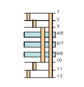
A crucial concept here is the “order” or “step” of an HDI board, often described by formulas like a+N+a or a+N+N+a.
a stands for the Build-up layer, which is formed using laser microvias. Each additional build-up layer on one side counts as one “step” or “order”.
N stands for the Core layer, which is a traditional multilayer PCB with through-holes or buried vias. The value of N indicates the number of conductive layers within the core. For example, a 4-layer core is N=2 (counting internal layers), and an 8-layer core is N=4. This explains why “N” is often an even number.
Here is a clear outline of common HDI structures, from simple to complex:
1. 1+N+1 (1-Step HDI)
This is the simplest form of HDI. It features a single build-up of high-density interconnection layers on both sides of a core. This is a cost-effective entry point for adding HDI features, allowing for finer lines and microvias while keeping the process relatively straightforward.
2. 2+N+2 (2-Step HDI)
This structure involves two sequential HDI build-ups on each side. This allows for the use of stacked microvias (microvias placed directly on top of each other) or staggered microvias. It is ideal for designs requiring higher pin-count components and much greater routing density.
3. 3+N+3 and Beyond (3-Step / Any-layer HDI)
These are the most complex and advanced boards. They feature three or more sequential laminations, enabling “any-layer” interconnection, where virtually any layer in the board can be interconnected with microvias. This enables incredibly high component density and is used in cutting-edge applications like flagship smartphones, network servers, and medical imaging equipment.
HDI vs. Mechanical Blind/Buried Vias
It’s important to distinguish between laser-drilled HDI microvias and mechanically drilled blind/buried vias, as they represent different product types with distinct cost and capability profiles.
HDI (Laser Drilled):
Microvia Aperture: ≤ 0.15mm.
Characteristics: Uses laser drilling for high positioning accuracy, enabling very small apertures. Employs RCC (Resin Coated Copper) or laser-specific prepreg as dielectric material.
Applications: High-end miniaturized products.
Mechanical Blind/Buried Vias:
Aperture: Typically ≥ 0.2mm.
Characteristics: Uses mechanical depth-controlled drilling. Generally more cost-effective for larger diameter holes or high-volume production. Filled with resin or copper paste.
Applications: Applications requiring inter-layer connections but not the ultimate density.
Complex Structural Variations
HDI technology allows for complex combinations to meet specific design needs, such as stacked microvias, staggered microvias, and mixed structures combining laser and mechanical vias. These advanced configurations provide maximum design flexibility for the most demanding applications.
Beyond the Layer Count: Other HDI Product Forms
Furthermore, HDI technology is applied across various product forms to meet specific application needs:
HDI Rigid-Flex PCB Boards: Combine the durability of rigid boards with the flexibility of flexible circuits, using HDI technology to maximize density in the rigid sections and interconnection points.
Specialized High-Frequency HDI Boards: Utilize advanced dielectric materials with low loss tangent, combined with HDI design rules, to ensure signal integrity in high-speed digital and RF applications.
The goal of all these HDI PCB manufacturing products is always the same: to pack more performance and functionality into a smaller, lighter, and more reliable package. Understanding these types and structures helps in selecting the optimal product for your project’s specific needs, balancing complexity, performance, and cost.
What Is the Process of HDI PCB Fabrication?
The fabrication process for HDI PCBs is a highly precise and sequential operation that involves multiple cycles of lamination, drilling, and plating. This complex manufacturing process requires strict process controls and advanced equipment to achieve the high density interconnections characteristic of HDI boards. Here is the detailed manufacturing process of 3-Step HDI PCB:
Stage 1: Core Layer Processing
The foundation of HDI PCB starts with the core layer processing, which establishes the basic interconnection framework:
Panel Cutting – The process begins with cutting the base copper-clad laminate to the required size for panel processing.
Inner Layer Imaging – The circuit pattern is transferred to the core using photolithography with a dry film resist.
AOI (Automated Optical Inspection) – The imaged inner layer circuits are automatically inspected for defects like opens, shorts, or pattern irregularities.
Lamination – Multiple inner layers are bonded together with prepreg under heat and pressure to form the core structure.
Copper Reduction – Excess copper is chemically etched away to define the precise circuit traces.
Laser Drilling – Microvias with diameters ≤0.15mm are ablated using a precision laser drill system.
Mechanical Drilling – Through-holes are drilled mechanically for layer-to-layer connections.
Electroless Copper Deposition – A thin conductive copper layer is chemically deposited onto the entire panel, including the walls of all drilled holes.
Via Filling – The vias are filled with conductive paste or resin to create a flat surface for subsequent layers.
Stage 2: First Build-Up Layer (2nd Lamination Cycle)
The first HDI build-up layer adds additional interconnection density:
Inner Layer Imaging – Circuit pattern imaging for the first build-up layer using LDI (Laser Direct Imaging) for higher precision.
AOI (Automated Optical Inspection) – Comprehensive inspection of the imaged layer to ensure pattern accuracy.
Lamination – The first build-up dielectric layer is laminated onto the core structure.
Copper Reduction – Copper is etched to define the fine-line circuits on this layer.
Laser Drilling – Second-level microvias are drilled for the first build-up layer interconnection.
Electroless Copper Deposition – Copper deposition ensures proper conductivity in the new microvias.
Via Filling – The newly drilled microvias are filled to maintain surface planarity.
Dielectric Thickness: Consistent dielectric layer thickness control for impedance management
This precise, multi-cycle manufacturing process enables the creation of sophisticated HDI PCBs that meet the demanding requirements of modern electronic devices, providing the high density interconnections necessary for advanced applications while maintaining reliability and performance standards.
Why Choose an HDI PCB Manufacturer in China?
Selecting a manufacturing partner is a strategic decision. For many global companies, partnering with a HDI PCB manufacturer in China offers a distinct competitive edge. This advantage stems from a powerful combination of factors:
Unmatched Supply Chain Ecosystem: China’s concentrated electronics industry means HDI PCB manufacturing suppliers have immediate access to high-quality raw materials and components, reducing logistics costs and delays.
Concentrated Expertise and Experience: The region has been at the forefront of PCB production for decades. Many HDI PCB manufacturing factories possess deep, practical knowledge gained from handling countless complex projects.
Significant Investment in Advanced Technology: To stay competitive, leading Chinese manufacturers heavily invest in state-of-the-art equipment, such as advanced laser drilling machines and automated inspection systems.
Excellent Cost-Effectiveness: The scale of manufacturing and efficient operations allows for competitive pricing without compromising on quality, offering outstanding value.
Integrated Services (One-Stop Shop): Many leading HDI PCB manufacturers in China offer integrated services, from HDI PCB fabrication to full HDI PCB assembly. This simplifies your supply chain and accelerates time-to-market.
EBest Circuit (Best Technology) is a leading specialist in manufacturing complex 3-Step HDI (High-Density Interconnect) PCBs. With over 19 years of industry experience and a monthly production capacity of 28,900 square meters, we have the expertise and scale to bring your most advanced electronic designs to life.
Our focus on precision engineering and rigorous quality control makes us the ideal partner for industries where miniaturization, high speed, and reliability are critical, including:
Advanced telecommunications
Medical electronics
High-performance computing
A 3-Step HDI process involves three sequential lamination cycles, enabling highly complex interconnect architectures essential for modern, compact, high-pin-count devices.
This advanced capability allows for:
Stacked or staggered microvias
Efficient routing under fine-pitch BGAs
Enhanced signal integrity
These features are crucial for designing boards that meet the demands of next-generation electronics. To ensure the highest quality, we utilize state-of-the-art equipment, including Automated Optical Inspection (AOI) and Laser Direct Imaging (LDI). These systems allow us to deliver 3-Step HDI PCBs that consistently meet the strictest performance standards.
Why Choose EBest Circuit (Best Technology) for HDI PCB Manufacturing?
Selecting the right manufacturing partner is crucial for the success of any HDI PCB project. It requires a blend of advanced technical capabilities, a commitment to quality, and a service-oriented approach. EBest Circuit (Best Technology) offers a compelling combination of these factors, providing a reliable and efficient manufacturing experience.
Here are the key reasons to partner with us for your HDI needs:
Full Turnkey Solution and Extensive Experience: We simplify your supply chain by offering a comprehensive one-stop service. From initial PCB design and DFM (Design for Manufacturability) advice to component sourcing, PCB assembly, and final box build, we manage the entire process. Founded in 2006, our 19 years of experience mean we have the expertise to anticipate challenges and ensure your project’s success from concept to completion.
Uncompromising Quality and Certifications: Quality is embedded in our operations. We hold internationally recognized certifications, including ISO9001:2015, IATF16949, and ISO13485:2016, which validate our commitment to consistent quality management systems. Our strict quality control procedures cover every stage of production, from raw material inspection to final electrical testing, ensuring every HDI board we deliver is reliable and high-performing.
Advanced Technical Capability and Engineering Support: Our technical capabilities, detailed in the section below, are tailored for advanced HDI manufacturing. Beyond machinery, we provide dedicated one-on-one engineering sales support. This service ensures that your design is optimized for manufacturability and cost-effectiveness before production begins, reducing time-to-market and avoiding potential issues.
On-Time Delivery: We are committed to offering high-quality PCB solutions through efficient production and cost management. Furthermore, we understand the importance of deadlines. Our streamlined processes and online WIP (Work In Progress) updates ensure 97% on-time delivery, allowing you to plan your projects with confidence.
To sum up, our blend of technical expertise, quality assurance, comprehensive service, and reliable delivery makes us the ideal choice for your demanding HDI PCB requirements.
Technical Capability for HDI PCB Design
To ensure the successful manufacture of your High-Density Interconnect (HDI) printed circuit boards, designing within specific technical parameters is crucial. The following details EBest Circuit (Best Technology)’s comprehensive manufacturing capabilities, which are designed to guide your design process effectively. The data presented reflects our standard production capabilities as well as our advanced limits for specialized or prototype projects.
1. Laser Drilling & Microvia Capability
The foundation of HDI technology lies in creating microvias. Our advanced laser drilling technology ensures high precision and reliability for the most demanding designs.
Laser Drill Minimum Diameter: Our standard capability is 0.10mm, with a limit of 0.070mm available for prototype orders.
Microvia Aspect Ratio: We support an aspect ratio of up to 1:1, which is essential for creating reliable, high-density interconnects.
Microvia Copper Thickness: We maintain a standard copper thickness of ≥ 15μm within microvias to ensure excellent electrical conductivity and long-term reliability.
2. Fine Line & Space Technology
HDI designs require dense routing to accommodate complex circuitry in a compact space. Our advanced imaging and etching processes support the following minimum trace and space widths (based on client original artwork):
Inner Layer (1/1 OZ base copper):
Standard Capability: 4/4.5 mil (line/space)
Limit Capability: 3.5/3.5 mil (line/space)
Outer Layer (1/1 OZ base copper):
Standard Capability: 3.5/4 mil (line/space)
Limit Capability: 3/3 mil (line/space)
3. Layer Stack-Up and Registration Accuracy
Managing complex layer structures with high precision is critical for multi-step HDI boards. Our capabilities ensure perfect alignment and integrity throughout the stack-up.
Maximum Manufacturing Layers: We routinely produce boards with up to 50 layers, and have the capability to support designs of up to 100 layers, subject to a technical review to ensure optimal quality.
Layer-to-Layer Registration Accuracy: We achieve a standard registration accuracy of ≤ 0.15mm, with a high-precision limit of ≤ 0.13mm. This exceptional alignment is critical for the success of complex 3-Step HDI designs with stacked or staggered microvias.
4. Material Expertise for HDI Applications
We are proficient in processing a wide range of high-performance materials to meet the electrical and thermal requirements of various HDI applications.
Standard & High-Tg FR4: We offer a range of materials suitable for general use and thermally demanding applications, ensuring board stability under high operating temperatures.
High-Speed/Low-Loss Materials: For designs where signal integrity is paramount, we work with leading material brands such as Rogers, Taconic, and Isola to minimize signal loss and maintain integrity in high-frequency applications.
All in all, by designing within these proven capabilities, you can ensure your HDI PCB is both highly manufacturable and reliable. Leveraging EBest Circuit (Best Technology)’s advanced engineering and production expertise allows you to push the boundaries of innovation while minimizing risk, ensuring your product achieves its full performance potential.
Laser Drilling Machine for HDI PCB Manufacturing in China
The microvia is the cornerstone of any HDI board. Creating these tiny, precise holes reliably and consistently requires one key piece of technology: an advanced laser drilling machine.
Here’s why this investment is critical for quality in HDI PCB manufacturing in China:
Precision at Micro-Scale: Our laser drilling systems can create microvias with diameters smaller than 100 microns (0.1mm) with exceptional accuracy. Mechanical drills simply cannot achieve this level of fineness.
Clean and Consistent Holes: The laser creates clean, ablated holes without causing excessive stress or tearing in the surrounding material. This consistency is vital for reliable plating and electrical connection.
Enabler for High Density: This precision is what makes the high wiring density of HDI boards possible. It allows for the dense arrays of blind and buried vias that define advanced PCB HDI technology.
Our commitment to maintaining state-of-the-art laser drilling machine for HDI PCB manufacturing is a direct investment in the quality and capability we can offer our customers.
What Certifications Should a Reliable HDI PCB Manufacturing Factory Have?
Trust must be verifiable. International certifications are the clearest proof of a factory’s commitment to quality and reliability. When auditing potential partners, look for these key certifications:
ISO 9001: This certifies the company has an effective Quality Management System in place. It’s the fundamental baseline for a reliable operation.
IATF 16949: Essential for supplying the automotive industry, this standard focuses on continuous improvement, defect prevention, and reducing variation in the supply chain. It indicates a very high level of process control.
ISO 13485: This is specific to medical devices. Certification demonstrates that the manufacturer meets the stringent quality and traceability requirements critical for healthcare applications.
UL Listing: Underwriters Laboratories (UL) is a leading safety certification. A UL listing means the PCB materials and construction meet specific safety standards, which is often a requirement for products sold in North America.
At BEST Technology, we maintain these certifications not as mere badges, but as the operational framework for everything we do. They provide you with confidence that your products are built to last.
Case of Quick-Turn Wholesale HDI PCB Manufacturing by EBest Circuit (Best Technology)
A client required a batch of 8-layer HDI PCBs for a new networking device. The project faced two major constraints:
Time: Extremely short time-to-market demanded a quick-turn production cycle.
Performance: The design required high-density interconnects (HDI), impedance control, and high-Tg materials for reliability.
Traditional manufacturers often force a compromise between speed and advanced capabilities. This case illustrates how EBest Circuit (Best Technology) delivers both.
We tackled the challenge with a streamlined, application-focused workflow:
Rapid DFM Analysis
Within hours of receiving the files, our engineering team performed a Design for Manufacturability (DFM) check.
This proactive step identified potential production issues related to trace spacing and via design, preventing costly delays.
Material & Process Optimization
Immediately allocated high-Tg FR4 materials from stock.
Flexible production lines were configured for HDI processes, enabling a seamless transition from prototyping to full production.
Critical Process Execution
Laser Drilling: Achieved precise 0.10mm laser microvias for dense interconnections.
Fine-Line Imaging: Maintained consistent 3/3 mil inner layer trace/space to meet strict impedance requirements.
Controlled Surface Finish: Applied ENIG (Immersion Gold) on pads for superior solderability and Hard Gold Plating on connectors for durability.
Guaranteed On-Time Delivery: Quality control (AOI, E-test) ensured 100% reliability despite the accelerated schedule.
The success of this quick-turn HDI project relied on the following capabilities:
Advanced Material Support: Immediate access to high-Tg (>180°C), halogen-free, high-speed materials (e.g., Rogers, Taconic).
HDI & Micro-Via Expertise: Laser-drilled blind vias as small as 0.10mm.
High-Layer-Count Manufacturing: Ability to produce up to 32-layer boards.
Fine-Line Precision: 3/3 mil trace/space for complex, high-speed designs.
High Aspect Ratio Support: Through-hole aspect ratios up to 10:1 for reliable plating in thick boards.
Comprehensive Surface Finishes: ENIG, ENEPIG, Immersion Silver, Hard Gold, and more.
Precision Mechanical Machining: Tight outline tolerances of ±4 mil and expert gold finger bevelling.
EBest Circuit (Best Technology) merges rapid prototyping workflows with sophisticated HDI manufacturing. We are not just a supplier but a strategic partner, enabling clients to accelerate development without compromising performance or quality.
In conclusion, HDI PCB manufacturing is the critical engine behind the continued miniaturization and performance gains we see in modern technology. This guide has explored its processes, benefits, and what to look for in a manufacturing partner.
For your most demanding projects, you need a partner with proven expertise, advanced technology, and a commitment to quality. BEST Technology is that partner. We specialize in complex HDI, including advanced 3-step constructions, and rigid-flex boards. Pls contact us today at sales@bestpcbs.com for a personal consultation and a quick quote.
HDI PCB manufacturer is the first thing that comes to mind when high performance meets compact electronic design. With rising demand for compact and reliable products, HDI technology plays a key role in modern electronics. But how does HDI differ from regular PCBs? What makes a good HDI PCB manufacturer? And why are so many companies turning to India, USA, China, or even Europe for fabrication? In this blog, you’ll get answers to those questions and more.
EBest Circuit (Best Technology) offers pioneering HDI PCB manufacturing solutions for Cell phones, UMPC, MP3 Players, PMP, GPS, and other applications. Our solutions integrate advanced signal integrity analysis and impedance control (±5%) to meet 5G/millimeter wave and high-speed computing requirements. HDI PCBs in EBest Circuit (Best Technology) include standard HDI PCB, HDI flex PCB, 2-16 layers HDI multi-layer PCB, any layer HDI PCB, and rigid-flexible PCBs to high-frequency PCBs. ISO 9001, IATF 16949, ISO13485 & AS9100D certified manufacturing processes ensure aerospace-grade reliability. If you have any questions about HDI PCB design, HDI PCB prototyping, or HDI PCB assembly, let us know via sales@bestpcbs.com.
What is HDI for PCB?
HDI stands for High Density Interconnect. It’s a type of printed circuit board that has a higher wiring density per unit area than standard boards. In simple terms, HDI PCBs are more compact, but they carry more connections. This is made possible with microvias, blind vias, and fine traces.
Compared to regular boards, HDI PCBs support tighter designs, faster signal transmission, and lower power usage. These qualities are essential in smartphones, medical equipment, automotive electronics, and wearable tech. If space is limited, HDI is the answer.
The HDI PCB definition includes features like:
Laser-drilled microvias
Multiple layers
Fine line width and spacing
Higher pin count in smaller space
Because of these features, HDI is becoming standard in advanced electronics.
What is the difference between HDI PCB and standard PCB?
Via Types: HDI boards use microvias, blind vias, and buried vias. Standard boards use only through-hole vias.
Layer Count: HDI can have more layers in a thinner stack-up.
Lamination: Stack multiple layers with insulating layers between.
Testing: Conduct electrical tests to ensure quality and reliability.
The HDI PCB fabrication process demands cleanrooms, skilled technicians, and controlled environments. This is why choosing the right HDI PCB manufacturer is vital. EBest Circuit (Best Technology) is an original HDI PCB factory, with a monthly capability of up to 260,000 square feet (28,900 square meters), and more than 1,000 different boards will be completed. Warm welcome to contact us at sales@bestpcbs.com to discuss the HDI technology solutions for your projects.
What is the application of HDI PCB?
HDI boards are popular in sectors that need compact, high-speed, and multi-functional electronics. The most common HDI PCB application includes:
Also, flex PCB application often overlaps with HDI for folding or wearable designs. With more features packed into less space, HDI PCBs support innovation across industries.
Who is the manufacturer of HDI PCB in China?
China leads the global PCB market, with many strong HDI PCB manufacturer options. Some top names include:
EBest Circuit (Best Technology) – Known for precision HDI, flex, and RF PCBs.
Shennan Circuits – Large-scale production with global clients.
Suntak Technology – Strong in multi-layer and HDI designs.
Victory Giant – Offers high-quality PCB fabrication at scale.
Most of these companies also serve as PCB manufacturer in China for global OEMs. They provide competitive pricing, fast lead times, and complete design-to-delivery support. With 24/7 rapid prototyping (24-hour turnaround) and an on-time delivery rate of 97% delivery time rate in mass production, EBest Circuit (Best Technology) empowers global customers to achieve smaller form factors, higher reliability, and 2-3 weeks faster time-to-market across consumer electronics, automotive ADAS, and IoT ecosystems. EBest Circuit (Best Technology) empowers global customers to achieve smaller form factors, higher reliability, and 2-3 weeks faster lead time across consumer electronics, automotive ADAS, and IoT ecosystems.
HDI PCB Manufacturer in USA
If you prefer local support and fast logistics, many HDI PCB manufacturer in USA offer reliable options. Leading suppliers include:
TTM Technologies – One of the biggest US-based HDI producers.
Advanced Circuits – Known for prototype to volume HDI boards.
Sanmina – Serves aerospace, defense, and medical sectors.
The PCB fabrication USA market focuses on quality, IP protection, and technical collaboration. If your design is sensitive or requires close engineering support, the USA is a strong choice.
HDI PCB Manufacturer in India
India is rapidly growing in the electronics space. Several HDI PCB manufacturer in India offer both quality and affordability. Top names include:
AT&S India – Specializes in high-end HDI and advanced multilayer PCBs.
Shogini Technoarts – Offers flexible, rigid-flex, and HDI solutions.
Genus Electrotech – Supports mass production of HDI for local and export markets.
India’s rising strength in HDI electronics is driven by local demand, government support, and skilled labor.
HDI PCB Manufacturer in Europe
European companies often prioritize environmental standards and high precision. Reliable HDI PCB manufacturer Europe list includes:
AT&S (Austria) – Strong in HDI and IC substrate solutions.
NCAB Group (Sweden) – Provides engineering-focused HDI support.
Würth Elektronik (Germany) – Offers HDI, RF, and advanced PCB types.
Europe may not match Asia in volume, but it leads in innovation and tight specs.
How to Choose an HDI PCB Manufacturer?
Finding the right HDI PCB manufacturer takes more than price comparison. Here are some key tips:
Experience: Check how long they’ve worked with HDI designs.
Certifications: Look for ISO, UL, RoHS, and IPC standards.
Capabilities: Ensure they can handle microvias, stacked vias, fine traces.
Prototyping: Choose someone who can support you from prototype to mass production.
Support: Good communication matters. Ask for an HDI PCB manufacturer address to know their actual site.
Documentation: A good partner can offer design tips or an HDI PCB design guide pdf.
Also, consider whether they offer other tech, like RF PCB manufacturing or flex PCB manufacturing services. It helps if they can grow with your needs.
In conclusion, choosing the right HDI PCB manufacturer affects the performance, cost, and speed of your project. With HDI technology, the margin for error is slim. Whether you’re working with a HDI PCB manufacturer in China, India, the USA, or Europe, the key is to find a trusted, experienced partner.
At EBest Circuit (Best Technology), we specialize in HDI boards, flexible circuits, RF PCBs, and complex stack-ups with tailored solutions. We support customers worldwide with professional engineering, fast prototyping, and reliable delivery. Reach out to EBest Circuit (Best Technology) at sales@bestpcbs.com to get a free quote for your next HDI PCB need. We’re always here to help.