PCB manufacturing PCB manufacturing
Home > Blog

Copper Grounding Bus Bar

How to Choose Reliable Copper Busbar Manufacturers: A Complete Guide
Friday, January 23rd, 2026

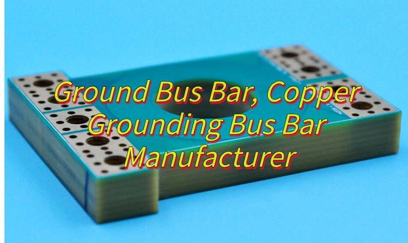
Selecting the right copper busbar manufacturers is critical for ensuring electrical system reliability and performance. High-quality copper busbar manufacturers adhere to strict material and process standards, while poor suppliers may cause energy loss, equipment failure, or project delays. This guide breaks down key factors to evaluate manufacturers and addresses common pain points in sourcing.

How to Select Reliable Copper Busbar Manufacturers?

Prioritize manufacturers with proven material quality, advanced processes, and industry certifications. Start by verifying copper purity (≄99.9% is ideal), checking customization capabilities, and confirming compliance with global standards like ASTM B187 and UL. Partnering with such manufacturers avoids mismatched specs and delivery risks.

Key Evaluation Criteria

  • Raw material sourcing: Ensure use of high-purity copper (C11000 ETP or C10200 OF grade)
  • Manufacturing equipment: CNC machining, automated bending, and precision stamping capabilities
  • Quality control: In-house testing for conductivity, mechanical strength, and corrosion resistance
  • Customer cases: Track record in EV charging, data centers, or renewable energy sectors

What Are the Core Quality Standards for Copper Busbar Manufacturers?

What Are the Core Quality Standards for Copper Busbar Manufacturers?

Top copper busbar manufacturers follow strict standards to guarantee product performance. The primary benchmark is ASTM B187/B187M, which defines dimensional, mechanical, and chemical requirements for copper busbars. Additional standards include RoHS for environmental compliance and ISO 9001 for quality management systems.

Must-Meet Standards

StandardKey Requirements
ASTM B187Copper purity, tensile strength, and dimensional accuracy
ULElectrical safety and fire resistance for industrial use
RoHSRestriction of hazardous substances in surface treatments

Why Material Purity Matters for Copper Busbar Manufacturers?

Copper purity directly impacts conductivity and durability. copper busbar manufacturers using 99.9%+ pure copper minimize energy loss (resistivity ≀1.7241 ΌΩ·cm) and reduce overheating risks. Low-purity copper with impurities degrades performance over time, leading to costly system failures.

Common Copper Grades for Busbars

  • C11000 (ETP): 99.93% pure, ideal for general industrial applications
  • C10200 (OF): 99.95% pure, superior conductivity for high-current scenarios
  • C12200 (DHP): For general-purpose applications requiring corrosion resistance

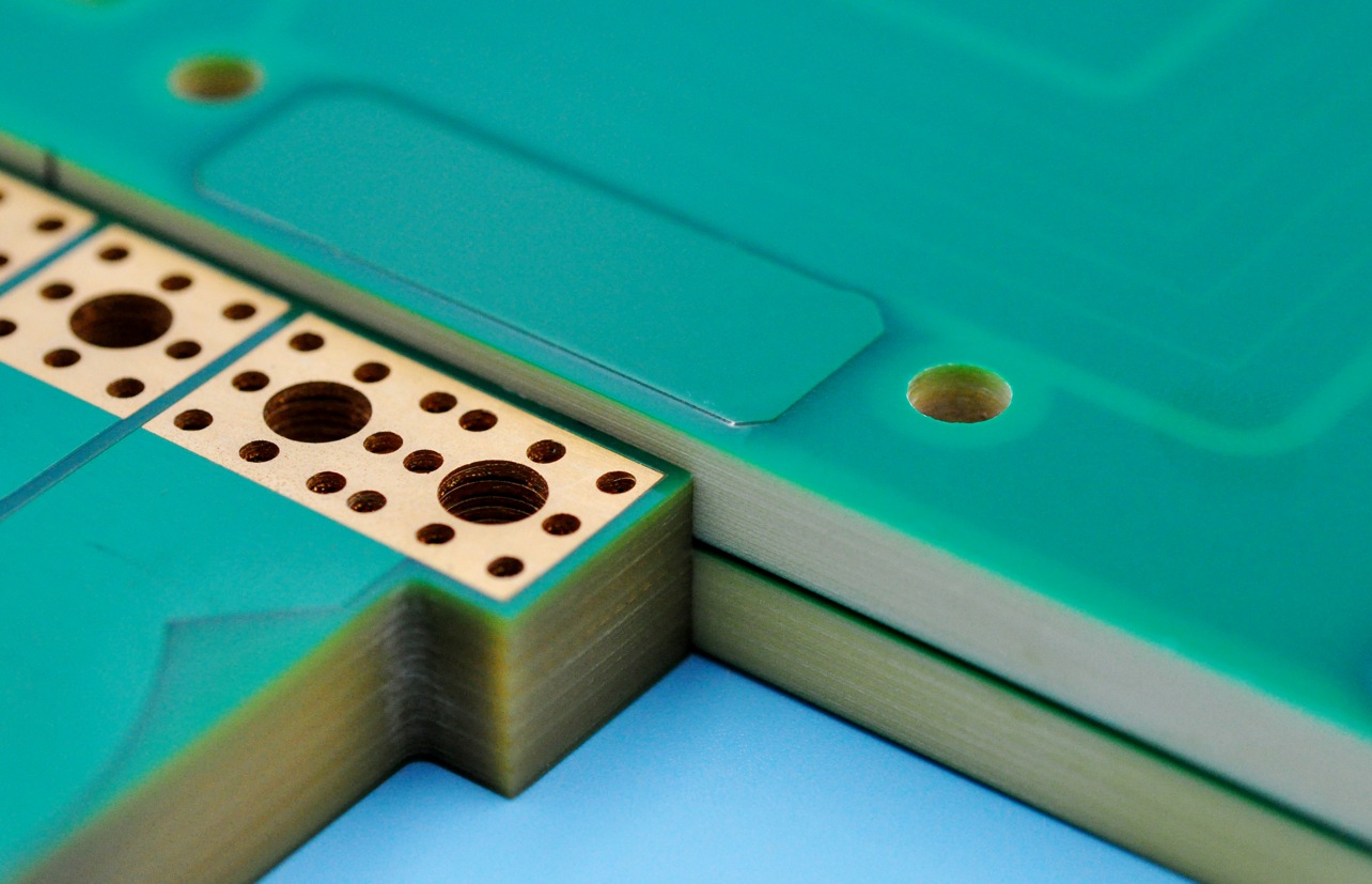
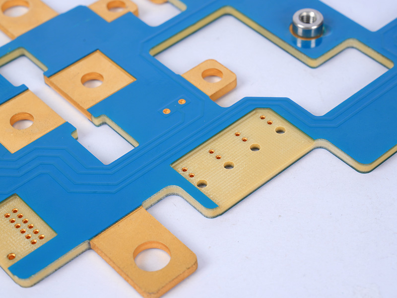
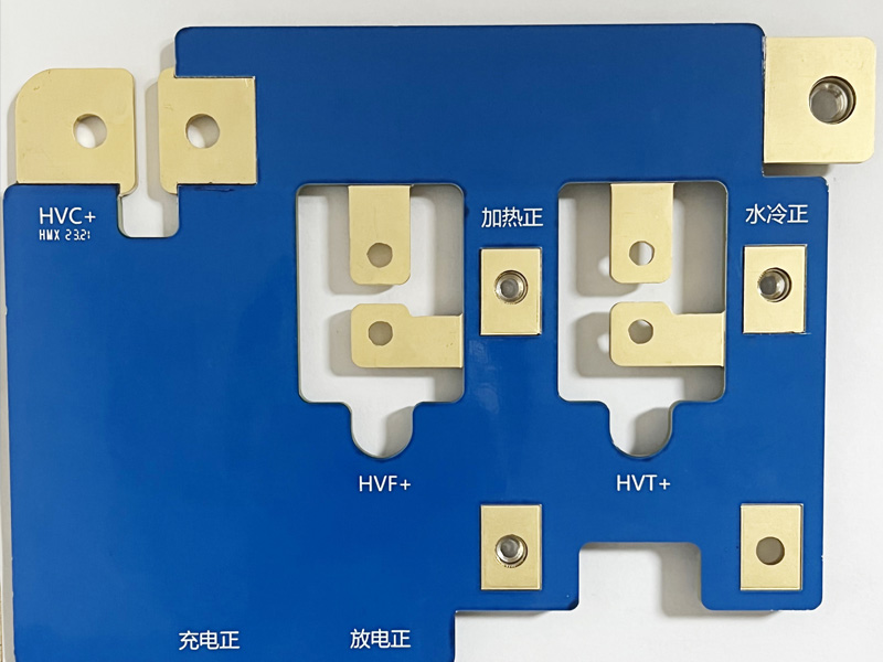
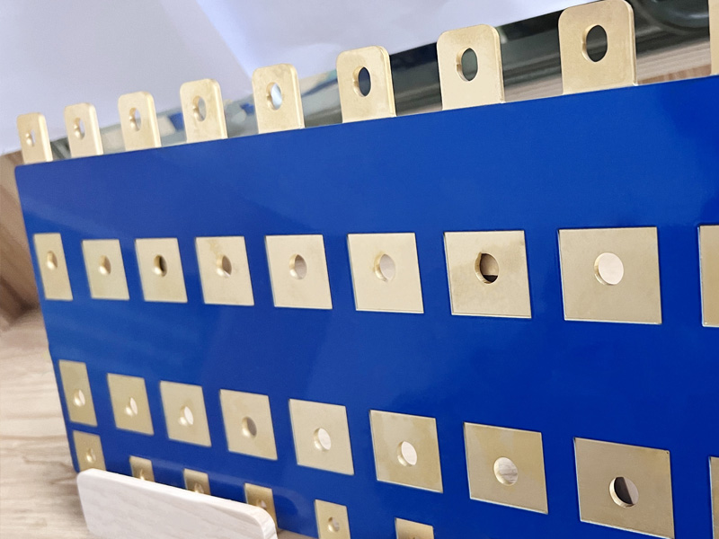
Customization Capabilities: Key Competitiveness of Copper Busbar Manufacturers

Reliable copper busbar manufacturers offer tailored solutions for unique project needs. This includes custom dimensions, shapes, surface treatments, and insulation options. Advanced manufacturers handle complex designs (e.g., laminated busbars) and adapt to tight tolerances (±0.05mm) for seamless system integration.

Customization Options

  • Dimensions: Custom width, thickness, and length (up to 6m)
  • Shapes: Bending, punching, and CNC-machined complex profiles
  • Insulation: Epoxy coating, heat-shrink tubing, or powder coating

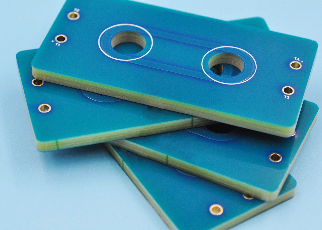
Surface Treatment Options from Top Copper Busbar Manufacturers

Surface treatments protect busbars from corrosion and enhance conductivity. Leading copper busbar manufacturers provide multiple finishing options to suit different environments, from humid industrial settings to clean data centers.

Popular Surface Treatments

  • Tin plating: Prevents oxidation, ideal for low-voltage applications
  • Nickel plating: Enhances wear resistance and solderability
  • Powder coating: Superior corrosion protection for outdoor use

How Do Copper Busbar Manufacturers Ensure Delivery Stability?

Delivery delays disrupt project timelines. Trusted copper busbar manufacturers maintain stable supply chains, keep inventory of standard specs, and offer clear lead-time commitments (7-15 days for standard orders, 2-4 weeks for custom). They also have backup production lines to handle unexpected demand.

Supply Chain Management Tips

  • Choose manufacturers with global raw material sourcing channels
  • Verify production capacity (minimum 100 tons/month for bulk orders)
  • Request clear delivery contracts with penalty clauses for delays

Industry Certifications to Verify Copper Busbar Manufacturers

Certifications are proof of a manufacturer’s expertise. Reputable copper busbar manufacturers hold ISO 9001 (quality management), IATF 16949 (automotive), and UL certifications. These credentials confirm compliance with global standards and reduce sourcing risks.

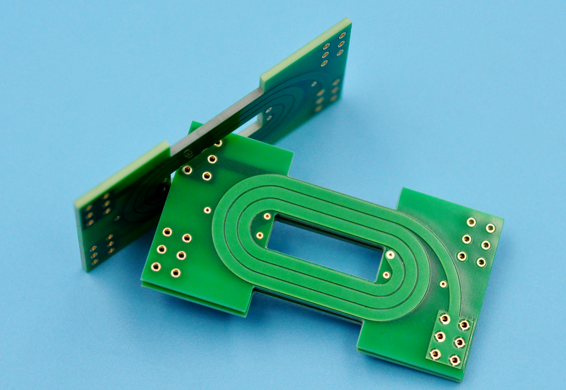
Differences in Manufacturing Processes Among Copper Busbar Manufacturers

Process gaps separate high-quality and low-grade copper busbar manufacturers. Advanced facilities use automated processes for consistency, while low-cost suppliers rely on manual labor (prone to errors). Precision machining ensures tight tolerances, avoiding fitment issues in assembly.

Process Comparison

  • Automated vs. manual: Automated processes reduce error rates to <0.5%
  • Heat treatment: Annealing (O60 temper) for flexibility or hardening (H04 temper) for strength
  • Testing: In-line conductivity testing vs. post-production sampling

Applications of Products from Copper Busbar Manufacturers

Copper busbar manufacturers supply components for diverse industries, where high conductivity and durability are critical. Key applications include EV charging stations, data center power distribution, renewable energy systems (solar/wind), and industrial machinery.

FAQ: Common Issues About Copper Busbar Manufacturers

Below are answers to frequent questions when sourcing from copper busbar manufacturers.

Q1: How to verify copper purity from manufacturers?

Request material test reports (MTRs) showing chemical composition. Reputable manufacturers provide MTRs compliant with ASTM standards, confirming copper purity ≄99.9%.

Q2: What is the typical lead time for custom busbars?

Most manufacturers deliver custom orders in 2-4 weeks. Rush orders (1 week) are available for urgent projects, often with a 10-15% premium.

Q3: Can manufacturers handle small-batch orders?

Yes, top manufacturers accept small batches (≄5 pieces) without compromising quality. Some offer discounted rates for repeat small orders.

Q4: How to resolve surface oxidation issues?

Choose manufacturers offering anti-oxidation treatments (tin/nickel plating). Post-delivery, store busbars in dry environments and avoid direct contact with corrosive substances.

Q5: Do manufacturers provide technical support for selection?

Reliable manufacturers assign engineers to assist with selection, based on current, voltage, and environmental requirements, ensuring optimal busbar design.

Q6: What certifications are mandatory for automotive busbars?

Automotive applications require IATF 16949 certification, along with RoHS compliance and UL 94 flammability ratings for insulation.

How to Evaluate the Cost-Effectiveness of Copper Busbar Manufacturers?

Cost-effectiveness goes beyond unit price. Evaluate total ownership cost, including quality (avoiding rework), delivery (preventing delays), and after-sales support. Cheap copper busbar manufacturers may cut corners on material or testing, leading to higher long-term costs.

Global Sourcing Guide for Copper Busbar Manufacturers

When sourcing globally, prioritize copper busbar manufacturers with local service centers to reduce logistics time and costs. US manufacturers excel in custom designs, while Asian suppliers offer competitive pricing for bulk orders. Always confirm import compliance with local standards.

We provide high-quality products from trusted copper busbar manufacturers, adhering to ASTM B187 and UL standards with customizable solutions for diverse industries. If you need reliable copper busbars, place your order with us via email at sales@bestpcbs.com.

Ground Bus Bar, Copper Grounding Bus Bar Manufacturer
Monday, August 18th, 2025

What is a ground bus bar for? Let’s explore its function, applications, working principle, production processes, design guide for ground bus bar.

Are you troubled with these problems?

  • Is the copper plate too thin, making it easy to burn through during welding? (Ground bus bar have a larger heat capacity and more stable welding.)
  • High-frequency current transmission losses are high? (Ground bus bar offer excellent conductivity and lower signal attenuation.)
  • Insufficient plate rigidity, making assembly prone to deformation? (Ground bus bar offer high strength, ensuring structural stability.)

EBest Circuit (Best Technology) can provide services + solutions:

  • Customized Processing Services – Precise cutting according to drawings, reducing secondary processing costs.
  • Fast Delivery Channel – 48-hour shipping for standard specifications, with priority scheduling for urgent orders.
  • Application Technical Guidance – Provide welding parameter recommendations and optimize production processes.

Welcome to contact us if you have any request for ground bus bar: sales@bestpcbs.com.

What is a Ground Bus Bar for?

A Ground Bus Bar (also known as Copper Grounding Bus Bar) is specialized circuit boards designed for efficient power distribution. By integrating solid copper or aluminum conductive traces (up to several millimeters thick), they can carry higher currents and are suitable for high-power applications. Unlike traditional PCBs that use etched copper wires to connect components, the core advantages of heavy copper PCBs lie in their high current-carrying capacity, mechanical strength, and space-optimized design. These advantages reduce heat generation and voltage drop, improve resistance to vibration and thermal cycling, and simplify wiring design.

What is a Ground Bus Bar for?

Where Do We Use a Ground Bus Bar?

Applications of ground bus bar:

  • New energy vehicle charging stations
  • Industrial inverters
  • Consumer electronics fast charging interfaces
  • Photovoltaic inverters
  • Energy storage converters
  • Rail transit traction systems
  • Substation grounding protection
  • Data center server cabinet power distribution units (PDUs)
  • Industrial motor controllers
  • Industrial robots

How Does a Grounding Bus Bar Work?

Providing a low-resistance grounding path

  • Thick copper plates (thickness ≄ 1.0mm) create a low-impedance path, quickly conducting fault currents in equipment casings or circuits to the ground, preventing voltage buildup that could damage equipment or cause electric shock.

Centralizing fault current distribution

  • Serving as the “central grounding point” of the electrical system, thick copper plates integrate multiple grounding wires to ensure even distribution of fault currents (such as short circuits and lightning strikes), preventing local overheating and arc flashovers.

Suppressing voltage fluctuations and electromagnetic interference

  • The large cross-section design of the thick copper plates reduces inductance effects, stabilizes the system reference potential, mitigates the impact of electromagnetic interference (EMI) on sensitive equipment, and ensures signal transmission quality.

Suitable for high-current scenarios

  • The high current carrying capacity (50A-300A) of thick copper plates (1.0mm-3.0mm) can handle the instantaneous high current demands of new energy vehicle charging and industrial motor starting, preventing circuit overheating or melting.

Mechanical and thermal stability

  • Thick copper structure resists vibration and temperature rise (copper thermal conductivity 400W/m·K), maintaining grounding reliability in high temperature or vibration environments, extending equipment life.

How to Make a Copper BusBar?

‌1. Material Preparation‌

  • Substrate Selection‌: Modified FR-4 or polyimide (PI) materials are chosen for their enhanced thermal stability and mechanical strength to withstand thick copper layers (typically ≄3oz/105ÎŒm)‌.
  • Copper Foil Preparation‌: Copper foils are selected based on current requirements (e.g., 2oz–12oz thickness), with surface treatments to improve adhesion‌.

2‌. Inner Layer Processing‌

  • Lamination‌: Copper foil is bonded to the substrate under controlled temperature/pressure (e.g., 180°C, 300psi) to prevent delamination‌.
  • Photoresist Application‌: Dry film resist is applied to define circuit patterns.
  • Exposure/Development‌: UV exposure transfers the design, followed by chemical development to remove unexposed resist‌.
  • Etching‌: Ammoniacal etchants are used with extended dwell times (20–30% longer than standard PCBs) to account for increased copper thickness. Sidewall compensation of 0.2mm–0.4mm is added to maintain trace accuracy‌.

3. Layer Stackup & Lamination‌

  • Prepreg Layering‌: High-resin-content prepregs (e.g., 2116 type) are used to fill copper thickness variations, ensuring 85%+ resin fill‌.
  • Multi-Layer Alignment‌: Optical targets align layers within ±25ÎŒm tolerance before pressing at 200°C/400psi for 90+ minutes‌.

4. Drilling & Metallization‌

  • Mechanical Drilling‌: Carbide drill bits with reduced feed rates (e.g., 1.2m/min for 4oz copper) minimize burring.
  • Hole Wall Roughness‌: <25ÎŒm to ensure plating uniformity‌.
  • Aspect Ratio‌: Limited to 8:1 for reliable plating‌.
  • Electroless Copper‌ Plating: Deposits 0.3–0.5ÎŒm seed layer.
  • Panel Plating‌: Electroplating builds copper to 25–30ÎŒm thickness with low-stress chemistry to prevent cracking‌.

5. Outer Layer Processing‌

  • Secondary Patterning‌: Repeat inner layer steps with adjusted exposure times for thicker resist‌.
  • Final Etching‌: Differential etching may be used for boards with mixed copper weights (e.g., 3oz signal traces + 8oz power paths)‌.

6. Solder Mask & Surface Finish‌

  • Solder Mask Application‌: Liquid photoimageable (LPI) solder mask is screen-printed or sprayed, then cured at 150°C for 45 minutes to withstand thermal stress‌.
  • ENIG (Electroless Nickel/Immersion Gold)‌: Common for high-reliability applications (e.g., 3–5ÎŒm Ni + 0.05–0.1ÎŒm Au)‌.
  • Hard Gold Plating‌: Used for edge connectors (e.g., 1–3ÎŒm Au over 5–10ÎŒm Ni)‌.

7. Electrical Testing & Inspection‌

  • Automated Optical Inspection (AOI)‌: Checks trace width/spacing with ±10% tolerance‌.
  • Flying Probe Test‌: Validates electrical continuity at 100–500V depending on design‌.

8. Final Processing & Packaging‌

  • Routing/V-Scoring‌: Diamond-coated cutters used for edge finishing; slower feed rates prevent copper tearing‌.
  • Cleaning‌: Ionic contamination controlled to <1.56ÎŒg NaCl/cmÂČ per IPC-6012‌. Packaging‌: Vacuum-sealed with desiccant for moisture-sensitive boards (>2oz copper)‌.
How to Make a Copper BusBar?

How to Design a Ground Bus Bar?

1. Strict Substrate Material Selection Criteria

  • FR-4 or high-TG laminate (such as Isola 370HR) is recommended. Its glass transition temperature (Tg) is ≄170°C, maintaining insulation stability over a wide temperature range of -40°C to 130°C. Experimental data shows that the interlayer peel strength of high-TG laminate reaches 12N/mm at 150°C, far exceeding the 8N/mm of standard FR-4.

2. Current-Carrying Capacity Quantification Model

  • Based on the IÂČR loss formula, a 4oz copper laminate with a width of 10mm can safely carry 150A. If the current increases to 200A, the copper thickness must be increased to 6oz or the width must be expanded to 25mm to ensure that the temperature rise does not exceed the industry standard limit.

3. Dynamic Cross-Sectional Area Optimization Strategy

  • Utilizing the “copper thickness-width” collaborative design principle: for every 100A increase in current, the copper thickness can be increased by 1oz or the width by 15mm. For example, for 300A requirements, a combination of 8oz copper thickness and 30mm width can be used, balancing cost and performance.

4. Practical Application of Voltage Drop Formula

  • Using the formula ΔV = I × R × L, when a 200A current passes through a 50mm long 8oz copper plate, the voltage drop can be controlled within 0.48V (ρ = 1.68 × 10⁻⁞ Ω·m). In actual designs, a 10% margin should be reserved to ensure the final voltage drop is less than 0.5V.

5. Wiring Topology Optimization Techniques

  • Adopting a “thickened main channel + thinned branch” design: Main lines must have a copper thickness of ≄ 6oz, and branches must have a copper thickness of ≄ 4oz. Combined with a grid-like ground layout, this design can reduce voltage fluctuations in high-frequency circuits to below 0.2V.

6. Stress Concentration Solution

  • Adding a 2mm radius to the bend area and combining it with a 0.8mm thick reinforcement plate can reduce the stress concentration factor at the bend from 3.2 to 1.5. Aperture design follows the “1.5 times the board thickness” principle. For 4oz boards, the recommended aperture is ≄1.5mm.

7. Thermal Via Array Design Specifications

  • Five thermal vias are required for every 100A of current. A 0.8-1.2mm diameter aperture is recommended, evenly spaced 3mm apart. Actual measurements show that this design can reduce hotspot temperatures by 18-25°C.

8. Temperature Rise Monitoring and Control

  • A three-stage test using an infrared thermal imager ensures: no-load temperature rise <10°C, half-load temperature rise <35°C, and full-load temperature rise <50°C. Temperature sensors are installed in key areas (such as under power devices) to ensure surface temperatures ≀90°C (UL standard).

9. Composite Heat Dissipation Structure Design

  • A “sandwich” layered design is employed: a top layer of thick copper (≄4oz) carries high current, a middle layer is filled with 3M 8810 thermal adhesive (thermal conductivity 1.5W/m·K), and a bottom layer houses high-frequency signal lines. This structure can reduce thermal resistance to 0.8°C/W.

10. Tolerance Control System

  • “Double Precision” control is implemented: copper thickness tolerance is ±10% (e.g., 3.6-4.4oz for a 4oz board), and hole position deviation is ≀0.1mm. An X-ray inspection system is used to ensure inter-layer alignment error is <0.05mm.

11. Surface Treatment Options

  • Tin plating (5-10ÎŒm) is suitable for high-temperature soldering applications and can withstand peak temperatures of 260°C. OSP treatment is suitable for no-clean processes and has a shelf life of up to 12 months. Both solutions have passed the 24-hour salt spray test (ASTM B117 standard).

11. Rigorous Electrical Performance Testing

  • Dielectric strength test: 500V AC for 1 minute without breakdown; contact resistance test: <5mΩ (four-point probe method). High-frequency signal layers must pass S-parameter testing to ensure insertion loss <0.5dB at 10GHz.

12. Mechanical Environmental Adaptability Verification

  • Vibration test: No cracking after 3g acceleration shock in the 5-2000Hz frequency range.
  • Thermal shock test: 100 cycles from -40°C to 125°C, with interlayer peel strength loss of <15%.
How to Design a Ground Bus Bar?

Why Choose EBest Circuit (Best Technology) as Copper Grounding Bus Bar Manufacturer?

Reasons why choose us as copper grounding bus bar manufacturer:

  • International Certifications: Hold ISO 9001 quality management system certification, UL safety certification, and IPC-6012 Level 3 standards. All thick copper clad products comply with RoHS/REACH environmental regulations, ensuring long-term reliability for industrial applications.
  • Specialized Ultra-Thick Copper Production Line: Equipped with a dedicated 4-20oz thick copper clad production line, this line utilizes pulse plating technology to ensure uniform copper thickness (≀15%) and a current carrying capacity of 20A/mmÂČ, eliminating the uneven plating issues often encountered in traditional processes.
  • Full-Process Intelligent Inspection: Deployed with an AOI + X-ray dual inspection system, this system achieves a 99.7% detection rate for defects such as voids and nodules in thick copper clad plating. Electrical testing covers 12 key parameters, including temperature rise and current carrying capacity.
  • High-Frequency Thick Copper Hybrid Process: Supports composite lamination of high-frequency materials and thick copper, achieving an impedance control tolerance of ±7%, meeting the high power and low loss requirements of applications such as 5G base station power supplies.
  • Industry Case Studies: Over 200 projects with 4oz+ copper thickness have been delivered in the past three years, including industrial-grade applications such as new energy inverters and rail transit power modules.
  • Quick-Response Design Support: 48-hour thick copper clad design and manufacturing (DFM) reports are provided. Our engineering team is capable of optimizing impedance control within ±5%, supporting customized design requirements.
  • Stable Delivery Capabilities: Our dedicated thick copper clad production line achieves a standard 15-day lead time (compared to the industry average of 25 days). Over the past 12 months, our on-time delivery rate has been 98.6%, and urgent orders can be shortened to just 7 days.
  • Transparent Cost Control: Utilizing an algorithm that optimizes copper foil utilization, our 4oz clad production costs are 12% lower than the industry average. Quotes include engineering and testing fees, with no hidden charges.
Why Choose EBest Circuit (Best Technology) as Copper Grounding Bus Bar Manufacturer?

Our Ground Bus Bar Capabilities

ParameterSpecification
Minimum distance between copper bars0.8-1.0mm
Copper thickness for bar1.0mm-3.0mm
Current carrying capacity50-300A
Surface finishingENIG, immersion silver, gold plating
Board thickness3.0-6.0mm
Hole wall thickness>=25um
Thickness to diameter ratio1:6 or 1:7 (for 1.0mm copper with a minimum of 0.7mm holes).
Layer counttypical 3-4 layers; additional layers possible with design evaluation
Maximum dimension600*400mm for standard bus bar PCB, 900*600mm for double sided PCB
lead time3-4L bus bar PCB is around 13-15days, add 3days per layer over 4 layers
Custom optionsSupport bending if customer has requirements

How to Get a Quote for Copper Grounding Bus Bar?

1. Basic Specifications

  • Dimensions (L x W x D, e.g., 24″ x 2″ x 0.25″)
  • Shape (Straight, L-shaped, U-shaped, Custom Bend)
  • Copper Thickness (e.g., 4oz, 5oz, 6oz)

2. Quantity and Delivery

  • Order Quantity (Sample, Small Order, Large Quantity)
  • Target Lead Time (e.g., “Within 3 Weeks” or “Expedited”)

3. Material and Process

  • Substrate Type (FR-4, Metal Substrate, Ceramic)
  • Surface Finish (Tin Plating, Galvanized Plating, Bare Copper)
  • Special Processes (e.g., Segmented Plating, Thick Copper Fill)

4. Certifications and Testing

  • Required Certifications (UL, ISO, RoHS)
  • Additional Testing (Salt Spray Test, High-Temperature Aging, Electrical Performance Testing)

5. Additional Requirements

  • Packaging Standards (Vacuum, Moisture-Proof, Wooden Rack Mounting)
  • Technical Documentation (CAD Drawings, 3D Models, Design for Implementation (DFM) Feedback)

Get an accurate quote now! Contact us today if you have any inquiry for copper grounding bus bar: sales@bestpcbs.com.