

The copper busbar manufacturing process combines heavy-copper PCB techniques with precise metalwork. It begins with careful design to control current and heat. Pure copper sheets or bars are cut, cleaned, and prepared for bonding.
During lamination or bar insertion, the copper forms a solid low-resistance path inside the PCB stack. CNC drilling and routing create exact holes and outlines. Plating with tin, nickel, or silver protects the surface and improves soldering.
Finally, each board is tested for conductivity, flatness, and insulation strength. This streamlined process delivers reliable, high-current PCBs for demanding power-electronics applications.
EBest Circuit (Best Technology) has nearly 19+ years of experience in PCB manufacturing, offering a one-stop service for bus bar PCBs from layout design, diagram evaluation, prototyping and mass production to after-sales service. We are certified by ISO9001, ISO13485, IATF16949, and UL, ensuring high-quality PCBs with fast delivery. As experts in bus bar PCB manufacturing, custom bus bar PCBs are available according to your specific requirements.
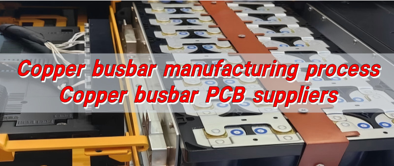
What is copper busbar PCB?
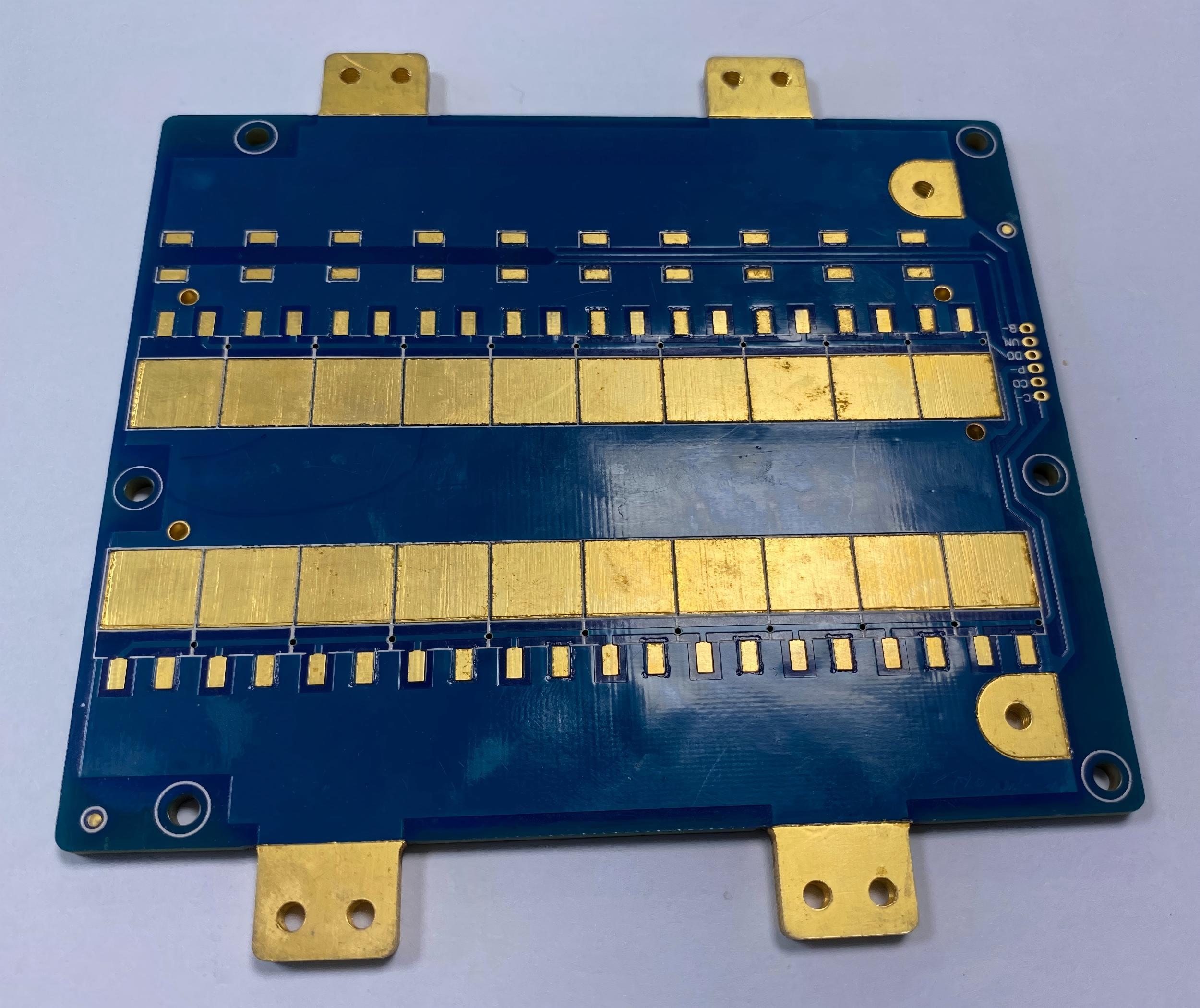
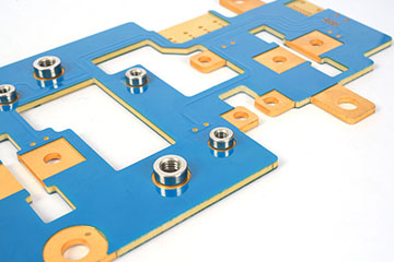
Copper busbar PCB is a printed circuit board with thick copper layers or inserted copper bars that move high current. It is different from a normal PCB.
Traditional boards handle small to medium current. A bus bar PCB carries far more power while keeping temperature under control.
Engineers place a solid copper bar or heavy copper layer inside the PCB stack-up. Applications include renewable energy systems, electric vehicles, industrial drives, and telecom power units. These fields need a safe, low-loss path for energy.
What is the raw material of copper busbar?
The key ingredient is pure copper with a high conductivity grade. Most manufacturers use C1100 or equivalent electrolytic tough pitch copper.
This type of copper contains more than 99.9% purity. It resists oxidation and carries current with minimal loss.
For insulation, makers use FR-4, polyimide, or other high-temperature PCB substrates. Epoxy resins with strong bonding power hold the layers together.
Surface finishes such as nickel, tin, or silver plating protect the copper from corrosion. The choice depends on the end use.
BEST Technology sources these materials only from certified producers. Stable raw stock ensures each busbar meets strict electrical and mechanical requirements.
How to make a copper busbar?
The copper busbar manufacturing process blends PCB technology with precision metalwork. Here is a clear view of the main stages:
- 1. Design and Simulation
Engineers design the current path and thickness. They run thermal and electrical simulations.
- 2. Copper Cutting and Preparation
High-purity copper sheets or bars are cut to exact size. Any surface oxide is removed.
- 3. Lamination or Bar Insertion
Two common methods exist.
Heavy copper lamination adds extra copper layers during PCB pressing.
Bar insertion places a pre-machined copper bar inside the board.
Both create a strong, continuous conductor.
- 4. Drilling and Routing
Precise CNC drilling forms mounting holes and routing channels.
- 5. Plating and Surface Finish
Nickel, tin, or silver is plated on exposed copper. This guards against oxidation and improves solderability.
- 6. Solder Mask and Legend
A protective solder mask covers non-conductive areas. Markings identify polarity and connection points.
- 7. Testing and Inspection
Manufacturers test current capacity, insulation resistance, and thermal rise. Only boards that meet design specs move forward.
Each stage demands strict process control. High-power electronics cannot tolerate flaws. Experienced copper bus bar manufacturers BEST TECHNOLOGY use advanced equipment to keep every parameter consistent.
What matters most in Copper Bar Production for PCBs?
Several factors decide final quality:
- Conductivity: Copper purity is critical.
- Thickness: Adequate thickness handles the required amperage without excessive heat.
- Flatness: Perfectly flat bars ensure tight contact with PCB layers and connectors.
- Plating Quality: Uniform plating prevents corrosion and maintains low contact resistance.
- Dimensional Accuracy: Power modules need precise fit.
- Thermal Management: Designers must plan for heat spread and airflow.
Reputable copper busbar manufacturers BEST TECHNOLOGY will monitor these points during the manufacturing process.
Basic parameter of Bus Bar PCB Manufacturing
Key specifications often include:
| Specification | Details |
| Minimum distance between copper bars | 0.8 – 1.0 mm |
| Copper thickness (bars) | 1.0 – 3.0 mm |
| Current carrying capacity | 50 – 300 A |
| Bending capability | Copper bars can be bent per customer requirements |
| Surface finishing options | ENIG, immersion silver, gold plating |
| Board thickness | 3.0 – 6.0 mm |
| Hole wall thickness | ≥ 25 µm |
| Thickness-to-diameter ratio | 1:6 or 1:7 (for 1.0 mm copper with a minimum of 0.7 mm holes) |
| Typical layer count | 3 – 4 layers (more layers possible with design evaluation) |
| Maximum dimension (standard) | 600 × 400 mm |
| Maximum dimension (double-sided PCB) | 900 × 600 mm |
| Lead time (3–4 layers) | ~13 – 15 days |
| Extra lead time per layer >4 | +3 days per additional layer |
What are the advantages of Bus Bar PCB?
A bus bar PCB provides clear benefits compared with standard layouts:
- Lower Resistance: Thick copper or bars carry large current with minimal loss.
- Better Heat Control: Wide copper paths spread and release heat quickly.
- Compact Design: High current moves through smaller space, reducing overall footprint.
- High Reliability: Strong copper core resists fatigue and vibration.
- Cost Efficiency: Fewer parallel traces and connectors lower assembly time.
These advantages matter in heavy-duty power electronics. Solar inverters, battery systems, and EV chargers need reliable high current flow every day.
Why should you use a bus bar PCB for power electronics?
Power electronics depend on efficient current distribution. A bus bar PCB cuts energy loss and enhances thermal performance.
Instead of routing multiple wide traces, designers integrate a single copper bus. This reduces connection points and lowers risk of loose joints.
The solid copper path also handles sudden current spikes. Equipment stays stable under load changes.
Maintenance becomes simpler. The board lasts longer with fewer hot spots and less stress on components.
What are the applications of Bus Bar PCB?
You will find bus bar PCBs across many industries:
- Electric Vehicles: Battery management and drive inverters.
- Renewable Energy: Solar power inverters and wind turbines.
- Industrial Equipment: High-power motor controls and automation systems.
- Telecom and Data Centers: Power distribution units for stable uptime.
- Medical Devices: Imaging systems that demand steady high current.
In every case, heavy copper boards secure strong performance and safe operation.
Conclusion:
Copper busbar PCB offers unmatched power handling, heat control, and reliability. From pure copper raw materials to careful plating, every step of the copper busbar manufacturing process must meet strict standards.
EBest Circuit (Best Technology) Co., Ltd. is one of the trusted copper busbar manufacturers with factories in China and Vietnam. We deliver quick lead times, high precision, and competitive pricing. Our team provides a free first sample and 24-hour technical response.
For detailed specifications or a custom quote, reach out to sales@bestpcbs.com