Copper busbar current carrying capacity (ampacity) is the maximum electrical current a copper busbar can safely conduct without overheating or failure, a critical parameter for electrical panel and power distribution design. Following ANSI C119.2 and IEC 60364 standards ensures copper busbar current carrying capacity meets industrial safety requirements, avoiding fire or equipment damage risks. This guide breaks down calculation methods, key influencing factors, and compliance checks for copper busbar current carrying capacity to help engineers make accurate decisions.
What Is Copper Busbar Current Carrying Capacity (Ampacity)?
Copper busbar current carrying capacity, also known as ampacity, refers to the maximum RMS current a copper busbar can carry continuously under specific environmental conditions (temperature, humidity, installation space). Unlike theoretical conductivity, practical ampacity accounts for heat dissipation, material resistivity, and long-term operational stability—key to preventing overheating in high-voltage applications.
How to Calculate Copper Busbar Current Carrying Capacity (Step-by-Step Formula)
The core formula for copper busbar ampacity calculation (per ANSI C119.2) is:
I = (k × A × ΔT^0.5) / L
– I = Current carrying capacity (amps)
– k = Material constant (5.7 for pure copper)
– A = Cross-sectional area (mm²)
– ΔT = Allowable temperature rise (°C, typically 30-60°C)
– L = Busbar length (meters)
This formula prioritizes real-world heat dissipation, not just theoretical conductivity. For 10x100mm copper busbars (1000mm²), the baseline ampacity is 2500A at 40°C ambient temperature—adjust for installation (air vs. enclosed) by ±15%.
Key Factors Affecting Copper Busbar Ampacity
Temperature (Ambient & Operating)
Ambient temperature directly impacts copper busbar current carrying capacity: every 10°C increase above 40°C reduces ampacity by 8-10%. For example, a copper busbar rated 2000A at 40°C only carries 1800A at 50°C. Operating temperature (from internal resistance) must stay below 90°C to avoid material degradation.
Busbar Size & Installation Method
- Thicker busbars (≥10mm) have 20% higher ampacity than thin ones (≤5mm) of the same width, due to better heat dissipation.
- Open-air installation increases ampacity by 15% vs. enclosed panels (common in switchgear).
Copper Busbar Current Rating Comparison (By Material/Thickness)
| Copper Busbar Specification | Cross-Section (mm²) | Ampacity at 40°C (A) | Ampacity at 50°C (A) |
|---|---|---|---|
| 5x50mm Pure Copper | 250 | 800 | 720 |
| 10x100mm Pure Copper | 1000 | 2500 | 2250 |
| 10x100mm Tinned Copper | 1000 | 2450 | 2205 |
Tinned copper busbars have slightly lower copper busbar current carrying capacity (2-3%) but better corrosion resistance—ideal for outdoor applications.
ANSI vs IEC: Copper Busbar Ampacity Standards Differences
ANSI C119.2 (US standard) uses 30°C ambient temperature as baseline, while IEC 60364 (EU standard) uses 40°C. This means a 10x100mm copper busbar rated 2600A per ANSI is only 2500A per IEC. Always align with regional standards to ensure copper busbar current carrying capacity compliance.
Common Mistakes in Copper Busbar Ampacity Calculation
- Ignoring ambient temperature: Using 40°C ratings for high-temperature environments (e.g., industrial plants) leads to 10-15% overload risk.
- Overlooking installation method: Enclosed panels require derating ampacity by 15%.
- Using theoretical conductivity instead of practical ampacity: Leads to inaccurate sizing and safety hazards.
FAQ: Copper Busbar Current Carrying Capacity (Engineer-Answered)
Q1: What is the maximum current a 10x100mm copper busbar can carry?
A 10x100mm pure copper busbar has a maximum copper busbar current carrying capacity of 2500A at 40°C (open-air installation). For enclosed panels, derate to 2125A; at 50°C, derate to 2250A.
Q2: How to adjust ampacity for high-temperature environments?
Use the temperature correction factor: For every 5°C above 40°C, multiply baseline ampacity by 0.95. For 60°C ambient, correction factor = 0.85 (2500A × 0.85 = 2125A).
Q3: Does coating affect copper busbar current capacity?
Non-conductive coatings (e.g., epoxy) reduce heat dissipation, lowering copper busbar current carrying capacity by 5-8%. Conductive coatings (e.g., tin plating) have minimal impact (≤3%).
Q4: What is the safety margin for copper busbar ampacity?
Industry best practice is a 15-20% safety margin: If your system requires 2000A, select a copper busbar with 2400A rated copper busbar current carrying capacity to account for voltage fluctuations and temperature spikes.
Q5: How to verify copper busbar ampacity compliance?
Use thermal imaging to check operating temperature (must be <90°C) and cross-verify with ANSI/IEC calculation formulas. Third-party testing (per UL 857) further validates compliance.
How to Select the Right Copper Busbar for Your Ampacity Needs
- Calculate required ampacity (including safety margin).
- Adjust for ambient temperature and installation method.
- Align with regional standards (ANSI/IEC).
- Choose material (pure/tinned copper) based on application environment.
Our engineering team provides free copper busbar current carrying capacity calculation support to ensure optimal sizing.
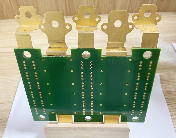
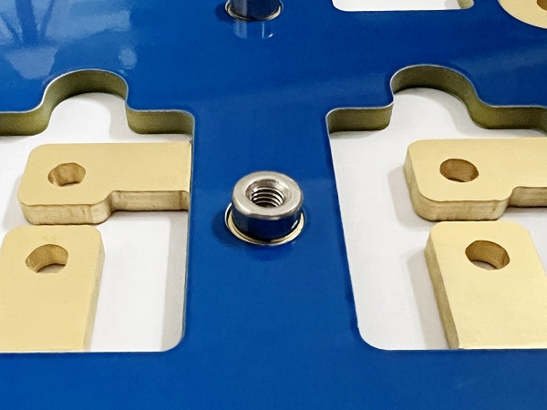
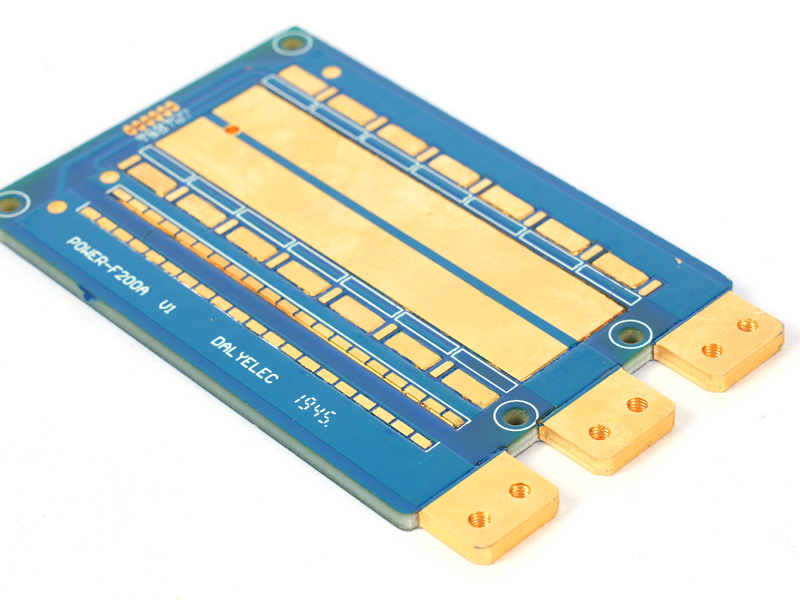
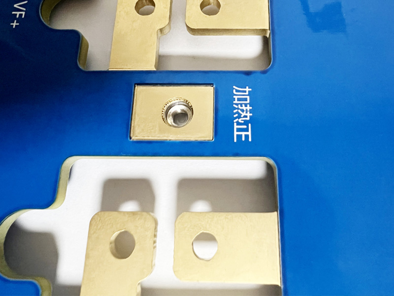
Our Copper Busbar Solutions for Reliable Current Carrying Capacity
We manufacture high-purity copper busbars (99.99% copper content) with precise copper busbar current carrying capacity ratings, compliant with ANSI and IEC standards. Whether you need custom sizes (5x50mm to 20x200mm) or tinned/epoxy-coated options, our products meet your exact ampacity requirements.
If you need reliable copper busbar current carrying capacity solutions for your electrical projects, place an order with us today. Contact our sales team via email: sales@bestpcbs.com.