

Automated optical inspection PCB solutions provide fast, accurate defect detection for PCBs, ensuring high quality and reliability in electronic manufacturing.
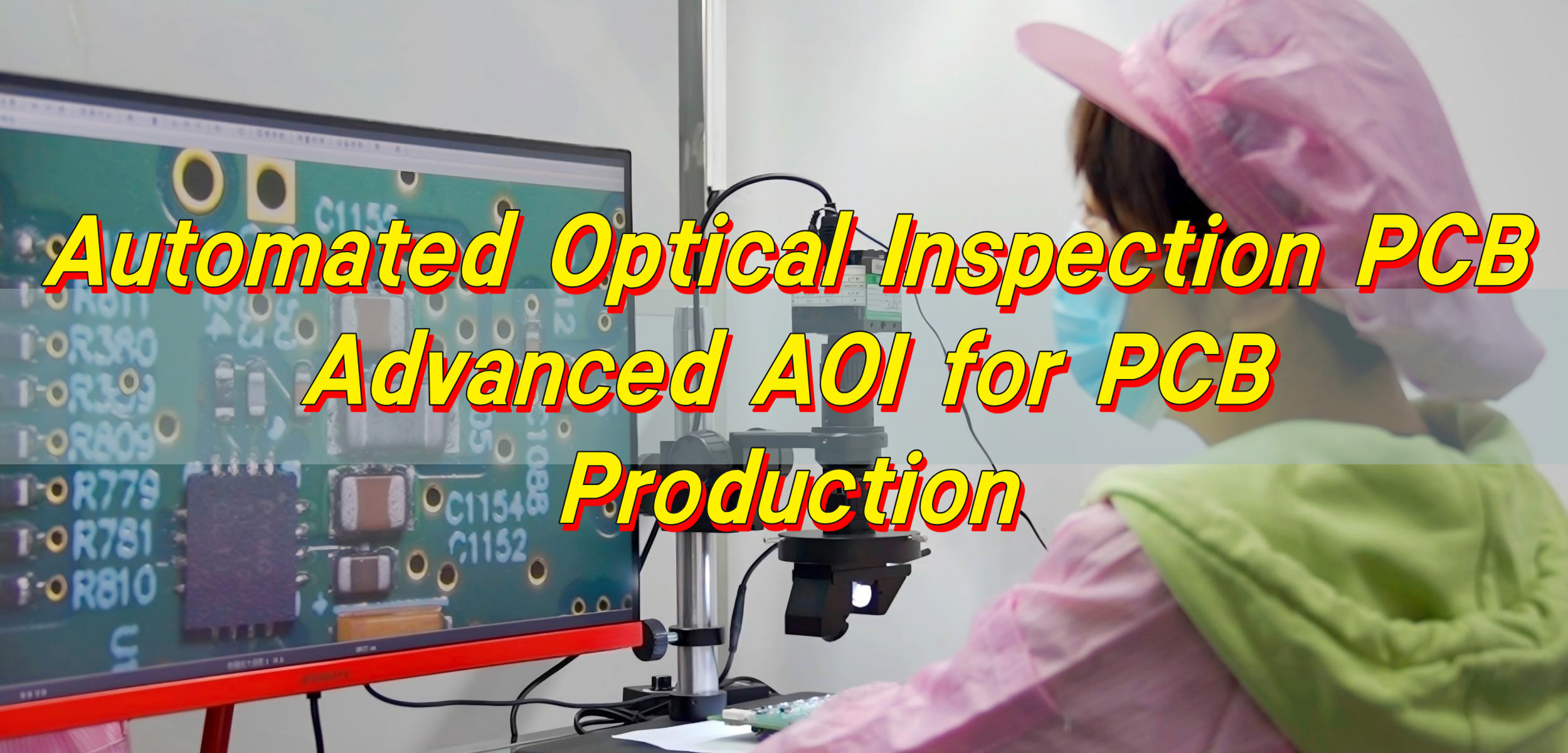
Automated optical inspection, commonly known as AOI, is a powerful inspection method that uses cameras, lighting systems, and software to check PCBs quickly and accurately. It plays a critical role in modern PCB assembly lines where thousands of boards are produced every day. With advanced imaging and intelligent analysis, AOI systems help detect defects early and improve production efficiency.
What is automated optical inspection PCB?
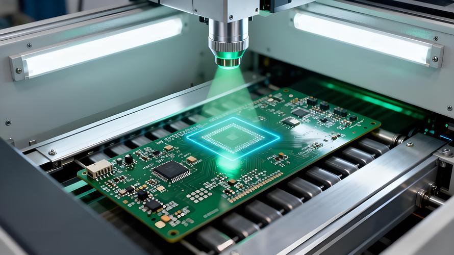
Automated optical inspection PCB refers to a computer-controlled inspection method used to evaluate printed circuit boards during manufacturing and assembly. The system uses high-resolution cameras and special lighting to capture images of a PCB and then compares those images with a predefined reference.
Instead of relying on manual inspection, AOI systems analyze each board automatically. The software checks component placement, solder joints, polarity, and other details to ensure every board matches the design requirements.
In modern electronics manufacturing, PCB automated optical inspection systems are widely used after solder paste printing, after component placement, and after soldering. Each inspection stage focuses on different aspects of board quality.
The inspection process usually involves several core elements:
- High-resolution cameras for image capture
- Precision lighting systems for contrast and clarity
- Image processing software to analyze patterns
- A comparison database containing the reference design
- Automatic defect classification tools
These systems allow factories to inspect thousands of boards every hour. The process is fast, consistent, and reliable. Because inspection results are stored digitally, engineers can also trace production issues and improve process control.
How does automated optical inspection work for PCBs?
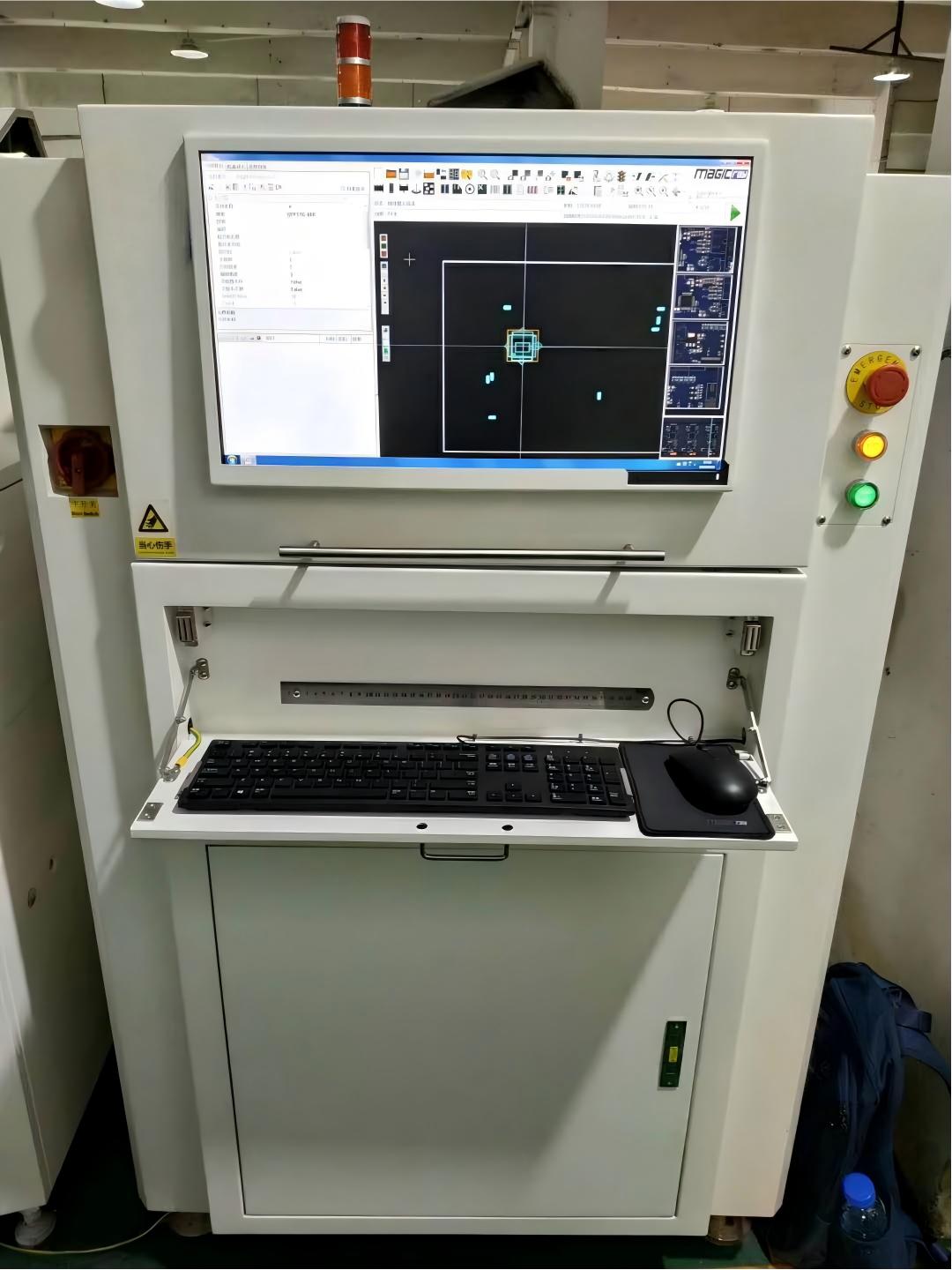
The automated optical inspection working principle is based on advanced imaging and pattern comparison. The system captures images of the PCB and analyzes them with specialized software to detect differences from the expected design.
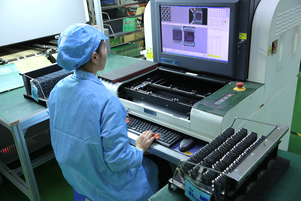
The inspection begins when a PCB enters the AOI machine on a conveyor. Cameras scan the entire board while controlled lighting highlights components and solder joints. The captured images are then processed by inspection software. The system compares the captured images with reference data generated from PCB design files or a known good board. When differences appear, the system flags them as potential defects.
The basic working stages include:
- Image capture using multiple high-resolution cameras
- Illumination control to highlight solder joints and components
- Image processing and pattern recognition
- Comparison with the reference design
- Defect detection and classification
Modern AOI systems also use multiple viewing angles. Some machines include 2D inspection cameras, while advanced models use 3D imaging to measure solder volume and component height. Because the inspection process is automated, the system maintains consistent accuracy across every board. Human inspection can vary depending on fatigue or experience, but automated optical inspection systems maintain stable performance throughout production.
Another advantage is data collection. Every inspection generates information about defects, process variation, and yield. Engineers can review this data to improve manufacturing processes and reduce recurring issues.
What is the process of AOI in PCB?
The PCB automated optical inspection process follows several stages during manufacturing. Each stage helps ensure that potential defects are detected as early as possible.
AOI inspection usually occurs at different points in the assembly process:
- Solder paste inspection stage
After solder paste is printed on the PCB pads, the board passes through an AOI system. The inspection checks paste alignment, volume, and coverage. Correct solder paste placement is important because it affects the quality of the solder joints.
- Component placement inspection
After components are placed on the board, AOI systems verify that each component is present and correctly positioned. The system checks orientation, polarity, and alignment.
- Post-reflow inspection
After the reflow soldering process, AOI performs a detailed inspection of solder joints and component connections. This stage identifies solder bridges, insufficient solder, and other assembly defects.
A typical AOI inspection flow includes:
- Board enters the automated optical inspection machine
- Cameras scan the PCB surface
- Software analyzes images in real time
- Detected issues are flagged for operator review
- Defective boards are removed for repair
This structured inspection process allows manufacturers to identify problems early. When defects appear in large quantities, engineers can quickly adjust the production parameters to solve the issue. Companies offering rigid-flex PCB fabrication services with automated optical inspection often integrate AOI into both fabrication and assembly stages. This ensures high reliability for complex PCB structures.
Why use automated optical inspection for PCB production?
Modern electronics manufacturing demands high precision and reliability. Even a small defect in a circuit board can cause device failure. Automated inspection helps manufacturers maintain strict quality standards while producing large volumes of boards.
Using automated optical inspection for PCB production provides several advantages compared with manual inspection.
First, AOI systems operate much faster than human inspectors. A modern automated optical inspection machine can scan hundreds of boards every hour with consistent accuracy.
Second, automated systems reduce the risk of human error. Visual inspection performed manually can miss small defects, especially during long production shifts.
Third, AOI systems improve traceability. Inspection results are stored digitally, allowing manufacturers to analyze trends and identify root causes of defects.
Some key reasons manufacturers rely on AOI include:
- High inspection speed for mass production
- Stable and repeatable inspection accuracy
- Early detection of manufacturing defects
- Reduced labor costs for inspection tasks
- Improved production data and process monitoring
AOI technology is particularly important for high-density PCB designs. Modern circuit boards contain many small components such as QFNs, BGAs, and chip resistors. These components require precise placement and soldering. Without automated inspection, verifying these tiny connections would be extremely difficult. AOI systems allow manufacturers to inspect them quickly and efficiently.
What defects can automated optical inspection PCB detect?
One of the strongest advantages of automated optical inspection PCB technology is its ability to detect many types of manufacturing defects. These defects can appear during solder paste printing, component placement, or soldering.
AOI systems identify visual differences between the manufactured board and the reference design. This allows the system to detect defects related to components, solder joints, and PCB structure.
Common defects detected by PCB optical inspection include:
- Missing components
- Misaligned components
- Incorrect component polarity
- Tombstoning of chip components
- Solder bridges between pads
- Insufficient solder joints
- Excess solder on pads
- Bent or damaged leads
- Incorrect component types
- PCB surface contamination
Because automated optical inspection systems analyze images at high resolution, they can detect even very small defects that are difficult to see manually. Some advanced AOI machines also support 3D inspection. This allows them to measure solder height and volume, which improves defect detection accuracy.
The following table shows common PCB defects and how AOI identifies them.
| Defect Type | Description | How AOI Detects It |
|---|---|---|
| Missing component | Component not placed on PCB | System compares component presence with reference design |
| Misalignment | Component placed off position | Image analysis checks placement accuracy |
| Polarity error | Component orientation reversed | Software compares orientation markers |
| Solder bridge | Solder connecting adjacent pads | Image contrast detects abnormal solder connection |
| Insufficient solder | Weak or incomplete joint | Inspection highlights low solder coverage |
| Tombstoning | One side of chip lifted | AOI identifies component angle differences |
What are the benefits of automated optical inspection PCB?
Using automated optical inspection PCB systems provides several operational and quality advantages. These benefits help manufacturers produce reliable circuit boards while maintaining efficient production.
One of the most important benefits is improved defect detection. AOI systems inspect every board in the production line, ensuring that issues are identified before products move forward. Another major advantage is production efficiency. Because automated inspection is fast, it keeps up with high-speed assembly lines without slowing the process.
Key benefits of AOI include:
- Higher product quality and reliability
- Faster inspection compared with manual methods
- Early detection of production defects
- Reduced repair costs
- Improved process control
- Consistent inspection accuracy
Another valuable benefit is process optimization. AOI data allows engineers to identify recurring problems in solder printing or component placement. Once these problems are identified, adjustments can be made to prevent future defects.
Many PCB manufacturers also integrate AOI results into their manufacturing execution systems. This allows real-time monitoring of production quality. For companies producing high-reliability electronics such as medical devices, automotive systems, and industrial equipment, automated inspection provides essential quality assurance.
How to choose automated optical inspection for PCBs?
Selecting the right automated optical inspection systems is important for achieving reliable inspection results. Different PCB products require different inspection capabilities.
Several factors should be considered when choosing an AOI solution.
First, the system resolution must match the complexity of the PCB design. Boards with small components require higher camera resolution.
Second, inspection speed should match the production line capacity. A slow inspection machine can create bottlenecks in manufacturing.
Third, the software capabilities must support accurate defect detection and classification.
Important selection factors include:
- Camera resolution and image quality
- Inspection speed and throughput
- Lighting technology for accurate contrast
- Software analysis and defect classification
- Compatibility with SMT production lines
- Support for 2D or 3D inspection
The table below compares two common AOI system types.
| Feature | 2D AOI System | 3D AOI System |
|---|---|---|
| Inspection method | Flat image analysis | Height and volume measurement |
| Detection ability | Good for placement defects | Better for solder inspection |
| Equipment cost | Lower | Higher |
| Application | Standard PCB assembly | High-density or complex boards |
Manufacturers should choose the system type that matches their product complexity and production goals. Companies providing rigid-flex PCB fabrication services automated optical inspection often combine advanced AOI with other inspection technologies to achieve higher reliability.
Where is automated optical inspection PCB used?
Automated optical inspection plays an essential role in many electronics industries. Because PCBs appear in almost every electronic device, AOI systems are widely used across manufacturing sectors.
Industries that rely heavily on PCB automated optical inspection include consumer electronics, telecommunications, automotive electronics, and industrial equipment.
Common application areas include:
- Smartphone and tablet manufacturing
- Automotive control modules
- Medical device electronics
- Communication equipment
- Industrial automation systems
- Aerospace electronic systems
AOI technology is also widely used in factories that produce rigid, flexible, and rigid-flex PCBs. These complex boards often require strict quality inspection due to their mechanical and electrical requirements. Manufacturers that provide rigid-flex PCB fabrication services with automated optical inspection ensure that flexible circuits and multilayer boards meet strict reliability standards.
In high-volume electronics production, AOI systems are often integrated with other inspection technologies such as X-ray inspection and electrical testing. Together, these methods provide comprehensive quality assurance.
How to optimize automated optical inspection for PCB quality?
Optimizing automated optical inspection for PCB quality requires careful setup and continuous improvement. Even advanced inspection machines perform best when properly configured and maintained.
One of the first optimization steps is creating accurate inspection programs. Engineers must define inspection parameters that match the PCB design and component specifications. Lighting configuration is another important factor. Proper lighting improves image contrast and allows the system to detect defects more clearly.
Best practices for optimizing AOI performance include:
- Creating accurate reference images
- Adjusting lighting angles for clear inspection
- Fine-tuning defect detection thresholds
- Regularly updating inspection programs
- Training operators to interpret inspection results
- Analyzing inspection data to improve production
Another important optimization strategy is integrating AOI data with manufacturing process control systems. This allows engineers to track defect trends and identify process changes that improve product quality.
At EBest Circuit (Best Technology), advanced inspection equipment and strict quality procedures ensure reliable PCB manufacturing. AOI systems are integrated into production lines to maintain high inspection accuracy and consistent product quality.
Summary:
Automated optical inspection has become an essential technology in modern PCB manufacturing. By combining high-resolution cameras, intelligent software, and fast inspection speeds, AOI systems help manufacturers detect defects early and maintain high production quality.
From solder paste inspection to final assembly verification, automated optical inspection PCB technology ensures that circuit boards meet strict performance standards. It improves production efficiency, reduces defect rates, and provides valuable manufacturing data.
Companies like EBest Circuit (Best Technology) integrate advanced inspection systems into PCB manufacturing and assembly services, ensuring high quality and consistent reliability for customers worldwide. If you would like to learn more about PCB manufacturing, automated inspection, or high-quality PCB solutions, feel free to contact our team. Email: sales@bestpcbs.com