

A 2 Layer SinkPAD board is a copper-based PCB structure designed for applications that need both strong thermal performance and more routing space on a compact layout. It features two circuit layers built on the same side of the board, combined with a dielectric insulation layer and a copper core or raised copper pedestal.
Unlike conventional metal core PCBs, the thermal pad of the LED in a 2 Layer SinkPAD board is placed directly on the copper core. This creates a direct thermal path, allowing heat to move away from the LED much faster. Because of this structure, the board is widely used in thermoelectric separation designs where electrical routing and thermal transfer need to be handled independently.
What Is a 2 Layer SinkPAD Board?
A 2 Layer SinkPAD board is a single-sided direct thermal path PCB with two copper trace layers arranged on the same side. Although it contains two routing layers, it is still considered a single-sided SinkPAD PCB because both circuit layers are located on the top side of the board.
The main advantage of this construction is that it combines electrical isolation with direct heat conduction. The circuit traces remain electrically insulated through the dielectric layer, while the LED thermal pad contacts the copper base directly.
Compared with a 1 Layer SinkPAD board, the 2-layer version supports more complex circuit routing on the same board size. That makes it a practical choice for compact, high-power lighting designs where both thermal control and circuit density matter.
2 Layer SinkPAD Board
How Does a 2 Layer SinkPAD Board Work?
The board works by separating the electrical path from the thermal path. Electrical signals move through the copper trace layers, while heat generated by the LED or power device is transferred directly into the copper core.
Since copper has very high thermal conductivity, around 400 W/m.K, heat can spread quickly from the hot spot to the base metal. From there, it can be transferred to a heatsink, mounting surface, or surrounding air. The direct contact design improves thermal efficiency far beyond what is possible with standard MCPCB structures. As a result, the LED junction temperature can be controlled more effectively.
Why Choose a 2 Layer SinkPAD Board Instead of a Standard MCPCB?
A standard metal core PCB usually includes a dielectric layer between the heat source and the metal base. That structure provides insulation, but it also adds thermal resistance. In a 2 Layer SinkPAD board, the thermal pad touches the copper pedestal directly, so heat does not need to pass through the dielectric in the same way.
This creates several practical benefits:
- Lower thermal resistance
- Better heat dissipation for high-power LEDs
- More stable light output
- Longer service life of the lamp
- Higher routing density on the same board area
- Better support for compact and advanced circuit design
For engineers working on high-power lighting modules, automotive lighting, or dense LED arrays, this structure offers a more efficient thermal solution without sacrificing design flexibility.
Advantages of Using 2 layers SinkPAD Board
- The metal core is Copper with high density, strong thermal carrying capacity and higher thermal conductivity. So the volume can be smaller under the same power.
- It adopts the thermoelectric separation structure, the Lumens depreciation of the LED is minimized, and the life of the lamp is prolonged.
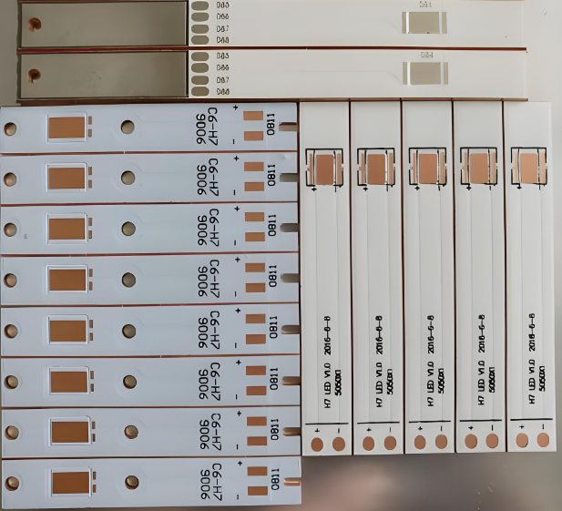
- Suitable for matching single high-power lamp, such as Cree XPL, XML, XHP; Osram LED, etc., also COB package LED
- High power semiconductors (transistors, thyristors, diodes) as well as resistors.
- A variety of Surface Finishing are available according to different demands. (ENIG, OSP, Immersion Tin, ENEPIG, HAL) with excellent reliability of the surface treatment layer.
- Different structures can be made according to different design needs of LED. (Such as copper bump, copper concave block)
- Put more circuits on the same side, design more complicated circuit board.
Typical Applications of 2 Layer SinkPAD Board
A 2 Layer SinkPAD board is commonly used in products that require both strong thermal conductivity and compact circuit design.
Typical applications include:
- High power LED modules up to 200W
- COB LED lighting
- Single high-power LEDs such as Cree XPL, XML, XHP, and Osram LEDs
- Automotive lighting systems
- Industrial lighting equipment
- Power semiconductor modules
- High-power resistor circuits
- Thermoelectric separation applications
Because of its copper direct thermal path structure, this board is especially useful in lighting products where heat buildup directly affects brightness consistency and service life.
2 Layer SinkPAD Board Stack-Up
The typical stack-up of a 2 Layer SinkPAD board includes:
- Two copper circuit trace layers on the same side
- Dielectric insulation layer
- Copper core or copper pedestal
- Direct thermal contact area under the LED thermal pad
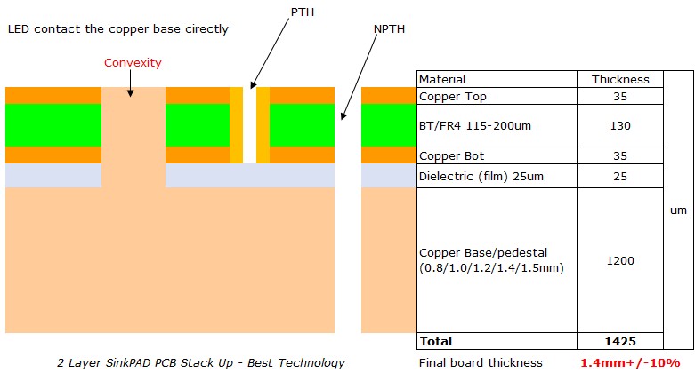
This stack-up is designed to achieve both electrical isolation and rapid heat transfer. It is one of the main reasons this board performs much better than ordinary aluminum PCB or traditional MCPCB in high thermal load applications.
Our 2 Layer SinkPAD Board Capability
| Item | Capability |
| Base Material | Copper |
| Copper Base Thickness | 0.8mm, 1.0mm, 1.2mm, 1.4mm, 1.5mm |
| Thermal Conductivity | 400 W/m.K |
| Board Thickness | 1.0mm to 2.0mm |
| Copper Thickness | 0.5 oz, 1 oz, 2 oz, special 3 to 10 oz |
| Outline Processing | Routing, Punching, V-Cut |
| Solder Mask Color | White, Black, Blue, Green, Red |
| Silkscreen Color | Black, White, Yellow |
| Surface Finish | Immersion Gold, ENEPIG, Immersion Tin, OSP |
| Max Panel Size | 600 x 500mm |
| Packing | Vacuum packing, plastic bag |
| Sample Lead Time | 1.5 to 2 weeks |
| Mass Production Lead Time | 2 to 3 weeks |
Why Is 2 Layer SinkPAD Board a Good Choice for High-Power LED Design?
In high-power LED products, heat is often the main factor that limits performance. Excessive temperature can reduce brightness, accelerate lumen depreciation, and shorten product lifespan. A 2 Layer SinkPAD board helps solve this issue by allowing heat to move directly into the copper base without unnecessary thermal barriers.
At the same time, the two-layer trace design gives more room for routing, which is useful when the LED module includes more complex circuitry. It is especially suitable for high-power LED modules, COB lighting, and power semiconductor applications where thermal performance directly affects reliability and lifespan. For projects that need both strong heat dissipation and more circuit freedom, a 2 Layer SinkPAD board is a highly effective choice.
FAQs about 2 Layer SinkPad MCPCB
1. What is a 2 Layer SinkPAD Board?
A 2 Layer SinkPAD Board is a high-power Metal Core PCB (MCPCB) that features two copper circuit layers on one side of a metal base. Unlike standard 2-layer MCPCBs where a dielectric layer separates all components from the metal core, the SinkPAD design “sinks” the thermal pad of a component through the dielectric, creating a Direct Thermal Path (DTP) to the copper or aluminum base.
2. How does a 2 Layer SinkPAD differ from a Single Layer SinkPAD?
While a single-layer SinkPAD only allows for simple circuit routing, a 2 Layer SinkPAD provides an additional copper layer for complex circuit design. This allows for more sophisticated power management, signal routing, or the placement of control components on the same board as high-power LEDs or transistors, all while maintaining the ultra-low thermal resistance of a direct-to-metal connection.
3. What are the thermal conductivity benefits of a 2 Layer SinkPAD?
Because the thermal pad of the component bypasses the 1–8 W/m·K dielectric layer and sits directly on the metal core, the effective thermal conductivity can reach 400 W/m·K (using a copper base). This is significantly higher than a standard 2-layer MCPCB, which is limited by the thermal resistance of the thin prepreg or dielectric layer required for circuit isolation.
4. Can I use Plated Through Vias (PTH) on a 2 Layer SinkPAD Board?
Yes, 2 Layer SinkPAD boards support inter-layer vias to connect the two copper circuit layers. However, these vias are typically used for electrical signals or low-power traces. The primary heat dissipation is still handled by the pedestal (the “SinkPAD”) that connects the high-power component’s thermal pad directly to the metal substrate, rather than relying on thermal vias.
5. When should I choose a 2 Layer SinkPAD over a standard FR4 with thermal vias?
You should choose a 2 Layer SinkPAD when your components generate heat that exceeds the capacity of FR4 (typically >3W per LED). While FR4 with thermal vias is cheaper, it cannot match the thermoelectric separation efficiency of a SinkPAD. If your application involves high-density power electronics where space is limited and active cooling is not an option, the 2-layer SinkPAD is the superior choice for reliability.
6. How does a 2 Layer SinkPAD differ from a Double-Sided SinkPAD PCB?
The primary difference lies in the circuit density versus mounting capability.
- 2 Layer SinkPAD: Features two copper circuit layers (Top & Bottom) on one side of the metal base. It is designed for complex circuitry that requires more routing space or inter-layer connections (vias) while still maintaining a Direct Thermal Path (DTP) for high-power components on the top side.
- Double-Sided SinkPAD: Features circuit layers and component mounting pads on both sides of the metal core (Top and Bottom). This allows you to mount high-power components, like LEDs or transistors, on both surfaces of the board, with each side utilizing the central metal core for heat dissipation.