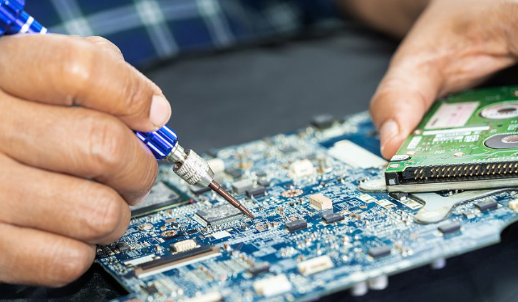
Burn-in test plays a critical role in electronics manufacturing where long-term reliability matters as much as performance. Engineers often rely on burn-in procedures to expose early-life failures before products reach the field. Whether used for high-reliability PCBA, industrial controllers, or medical electronics, this method helps stabilize product quality while reducing unexpected returns.
Below is a practical, engineering-focused guide explaining how burn-in testing works, why it matters, and how it applies specifically to PCB assemblies.
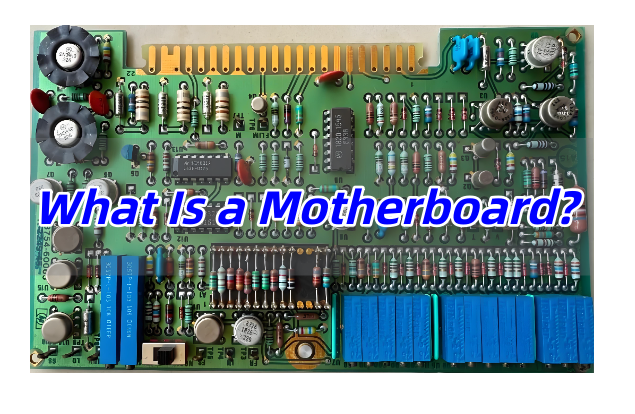
What Is a Burn-In Test in Electronics?
A burn-in test is a reliability testing process used in electronics manufacturing to identify early-life failures in electronic components, PCBs, and assembled electronic products.
During a burn-in test, electronic devices are operated under elevated stress conditions—such as higher temperature, voltage, or load—over a defined period of time. Components that are defective or marginal are more likely to fail during this phase rather than later in real-world use.
The primary purpose of a burn-in test is to improve product reliability and reduce field failures.
More specifically, burn-in testing is designed to:
Detect early-life failures (infant mortality)
Screen out defective components
Verify design robustness
Stabilize electrical performance
Reduce warranty returns and RMA costs
Electronics failures often follow the bathtub curve, where failure rates are high at the beginning, low during normal life, and rise again at end-of-life. Burn-in testing targets the first phase of this curve.
Why Is a Burn-In Test Important?
Burn-in testing plays a critical role in quality assurance (QA) and reliability engineering.
Key Benefits of Burn-In Testing
1. Reduces Early Field Failures
Burn-in tests catch problems such as:
Poor solder joints
Marginal ICs
Weak capacitors
Manufacturing defects
Thermal design issues
2. Improves Brand Reputation
Products that fail shortly after installation damage customer trust. Burn-in testing helps ensure only stable and reliable products ship.
3. Saves Cost in the Long Term
While burn-in testing adds upfront cost, it significantly reduces:
Warranty claims
Product recalls
Field repair costs
Customer downtime
4. Required by High-Reliability Industries
Industries such as medical, aerospace, automotive, and military electronics often require burn-in testing as part of regulatory or contractual standards.
How to Do a Burn-In Test?
A burn-in test procedure varies depending on the product, industry, and reliability requirements, but the core steps are similar. Typical burn-in test procedure including:
OurPCB assembly Lithuaniaservices deliver high quality by cutting lead times while upholding strict precision, directly helping businesses accelerate product launches without sacrificing performance. Our PCB assembly Lithuania solutions are aligned with EU RoHS directives and IPC assembly standards, solving the key need for efficient, compliant electronic manufacturing support in the Lithuanian and broader EU markets.
Faster Lead Times for Market Advantage: Our optimized local production lines reduce lead times by 30% compared to competitors, helping you shorten product time-to-market and gain a competitive edge, shortening small-batch order lead times from an industry average of 12 days to 8.4 days and prototype lead times to 3-5 days.
Comprehensive One-Stop PCBA Service: Our service covers DFM analysis, component sourcing, assembly, testing, and delivery, eliminating the need for multiple vendors and simplifying your project management for PCB assembly Lithuania, which reduces project cycle time by 25% on average and cuts vendor coordination costs by 35%.
Industry-Leading 5-Year Warranty: We provide a 5-year warranty for all our PCBA products, ensuring long-term reliability and reducing your post-delivery maintenance costs, with a 0.03% failure rate within the warranty period—far below the industry average of 0.5%.
Full Traceability via MES System: Our MES system enables real-time tracking of every step in the assembly process, from component arrival to final shipment, ensuring transparency and accountability for all PCBA orders, with 100% component lot traceability achievable within 30 seconds and production records retained for 7 years.
99.2% On-Time Delivery Rate: We consistently meet your project timelines with a 99.2% on-time delivery rate, minimizing delays and supporting your product launch schedule, and have maintained this high rate for 8 consecutive years, with urgent orders achieving an on-time delivery rate of 98.7%.
Effective Component Shortage Solutions: We leverage a network of 150+ local distributors and 300+ global partners, plus maintain safety stock of 500+ common components, to overcome component shortages for your PCBA needs, reducing component sourcing delays by 70% compared to the industry average and ensuring 99.5% component availability.
Strict Quality Control Processes: We mitigate quality risks through rigorous IQC, IPQC, and FQC inspections, adhering to ISO 9001, ISO 13485, and IPC standards for consistent PCBA quality, achieving a 99.92% first-pass yield (FTY) and rejecting only 0.08% of incoming components during IQC.
EU Compliance Assurance: All our PCBA services fully comply with RoHS, REACH, and other EU environmental and safety regulations, ensuring your products meet regional market requirements, having passed 12 consecutive EU compliance audits with zero non-conformities.
20 Years of Professional Expertise: With 20 years of experience in PCBA manufacturing, we possess deep expertise in handling complex PCBA requirements across diverse industries, serving over 5,000 clients globally and maintaining a 96% client retention rate.
How Do We Ensure On-Time Delivery Rate of Lithuania PCBA Orders?
Methods about we ensure on-time delivery rate of Lithuania PCBA orders:
Advanced Supply Chain Planning: Adopt AI-driven forecasting tools with 98.5% accuracy to predict component lead times, pre-order long-lead items (e.g., ICs, connectors) 45 days in advance, and reduce procurement delays by 80%.
MES Real-Time Tracking: Integrate MES systems to monitor key production milestones (mounting, soldering, testing) 24/7, detect bottlenecks within 15 minutes, and dynamically adjust schedules by linking with ERP systems for closed-loop management.
Flexible Production Scheduling: Prioritize urgent orders with a dedicated production queue, allocate 3 special SMT lines for rush tasks, and achieve quick line changeover (≤2 hours) to meet tight deadlines.
Reliable Logistics Partnerships: Cooperate with 3 top EU-focused carriers, realize 48-hour delivery to 27 EU countries, complete customs clearance within 24 hours via pre-customs filing, and ensure 72-hour delivery for international orders.
Buffer Time Allocation: Allocate 10% buffer time for small-batch orders and 20% for large-batch orders, reducing delivery delay risks to below 0.3% by accounting for unforeseen factors (e.g., equipment maintenance, customs fluctuations).
Proactive Communication: Sync order progress daily via email and instant messaging, issue delay warnings 48 hours in advance if risks arise, and provide 2+ alternative solutions (e.g., expedited production, alternative qualified components) promptly.
Pre-Production Risk Assessment: Conduct a 2-hour pre-production review for each order to check component availability, production capacity, and logistics feasibility, eliminating potential delivery obstacles upfront.
How We Control the Quality of PCB Assembly Lithuania?
Methods about we control the quality of PCB assembly Lithuania:
Incoming Quality Control (IQC): Conduct 100% inspection of all components, including visual checks, batch verification, and functional spot tests, to ensure authenticity, functionality, and compliance with IPC and RoHS standards, with only 0.08% of incoming components rejected.
Process Quality Control (IPQC): Perform hourly inspections during soldering, pick-and-place, and testing processes, focusing on placement accuracy (±0.03mm), soldering temperature profiles, and station operation compliance, with immediate shutdown and adjustment for any abnormalities.
Automated Inspection: Utilize AOI (coverage ≥99.5%) and X-ray machines to detect hidden defects such as bridging, poor solder joints, and internal voids in BGA/QFP components, with automatic defect marking and manual review for confirmation.
MES Traceability: Track every component lot, production equipment, operator, and inspection record via our MES system, enabling 100% traceability within 30 seconds and retaining records for 7 years to quickly locate and resolve quality issues.
Employee Training: Provide quarterly training on equipment operation, quality standard updates, and defect identification, with a post-training assessment pass rate of over 98% to ensure staff strictly adhere to quality requirements.
Equipment Calibration: Calibrate SMT, AOI, and testing equipment monthly per ISO 17025 standards, focusing on precision parameters (e.g., AOI detection sensitivity) to maintain accuracy, with a 100% calibration qualification rate.
Final Quality Control (FQC): Perform 100% functional and reliability tests on finished PCBs (including ICT and 24-hour aging tests) before packaging, achieving a 99.92% first-pass yield, with rework and re-inspection for non-conforming products.
Case Studies of Our Medical PCB Assembly Lithuania
Project Background: A Lithuania-based medical device company needed reliable Medical PCB Assembly Lithuania for its new portable diagnostic device, but struggled to find a partner meeting medical-grade quality and tight launch timelines.
Requirements: ISO 13485 compliance, IPC-A-610 Class 3, 500-unit order, 15-day lead time, low power consumption (standby ≥72h), and 0-defect tolerance.
Challenges: Tight 15-day lead time with medical-grade quality demands; miniaturized BGA/QFP components (0.5mm pin pitch, ±0.02mm precision); global shortage of specialized medical IC (procurement cycle >20 days); and full component/assembly traceability requirements.
Our Solution: One-stop PCBA service with DFM-based PCB layout optimization; specialized IC sourced via global network (delivered in 3 days); high-precision SMT equipment (±0.03mm accuracy); ISO 13485-compliant quality controls with MES tracking; dedicated production line and pre-delivery functional test.
Output Results: 100% on-time delivery (2 days early); 99.8% first-pass yield (1 defective unit replaced within 4h); 0 field failures in 12 months (meeting 0-defect demand); 30% shorter lead time and 12% lower costs vs previous supplier; 80% repeat order rate with 3 additional batches in 6 months.
Our Lithuania PCB Assembly Capabilities
Item
Capabilities
Placer Speed
13,200,000 chips/day
Bare Board Size
0.2 x 0.2 inches – 20 x 20 inches/ 22*47.5 inches
Minimum SMD Component
01005
Minimum BGA Pitch
0.25mm
Maximum Components
50*150mm
Assembly Type
SMT, THT, Mixed assembly
Component Package
Reels, Cut Tape, Tube, Tray, Loose Parts
Lead Time
1 – 5 days
FAQs of PCB Assembly in Lithuania
Q1: What is the typical lead time for PCB assembly in Lithuania? A1: Lead times vary by order size and complexity: prototype orders (10-50 units) take 3-5 days, small-batch orders (50-500 units) take 7-10 days, and large-batch orders (500+ units) take 15-30 days. We offer expedited services to cut lead times by 40% for urgent orders.
Q2: How do you ensure electronic components used in Lithuania PCB assembly are genuine? A2: We source components only from authorized distributors (local and global) with verified credentials. All components undergo IQC inspections, including visual checks, functionality tests, and batch verification. We also provide component traceability reports upon request.
Q3: Do you offer PCB assembly for medical devices in Lithuania, and what certifications do you hold? A3: Yes, we specialize in medical PCB assembly in Lithuania. We hold ISO 13485 certification (medical device quality management) and comply with IPC-A-610 Class 3 and RoHS standards. Our medical assembly processes meet EU MDR requirements for safety and reliability.
Q4: Can you handle small-batch PCB assembly orders in Lithuania, and is there a minimum order quantity? A4: We welcome small-batch and prototype orders with no minimum order quantity (MOQ). We have dedicated SMT lines for small-batch production, ensuring cost-effectiveness and fast turnaround even for orders as small as 1 unit.
Q5: What happens if a PCB assembly order is delivered late, and how do you compensate? A5: Our on-time delivery rate is 99.2%, and we proactively communicate any potential delays. For orders delivered late due to our fault, we offer a 5% discount on the total order value for each day of delay (up to 30% total). We also provide expedited rework to minimize impact on your project.
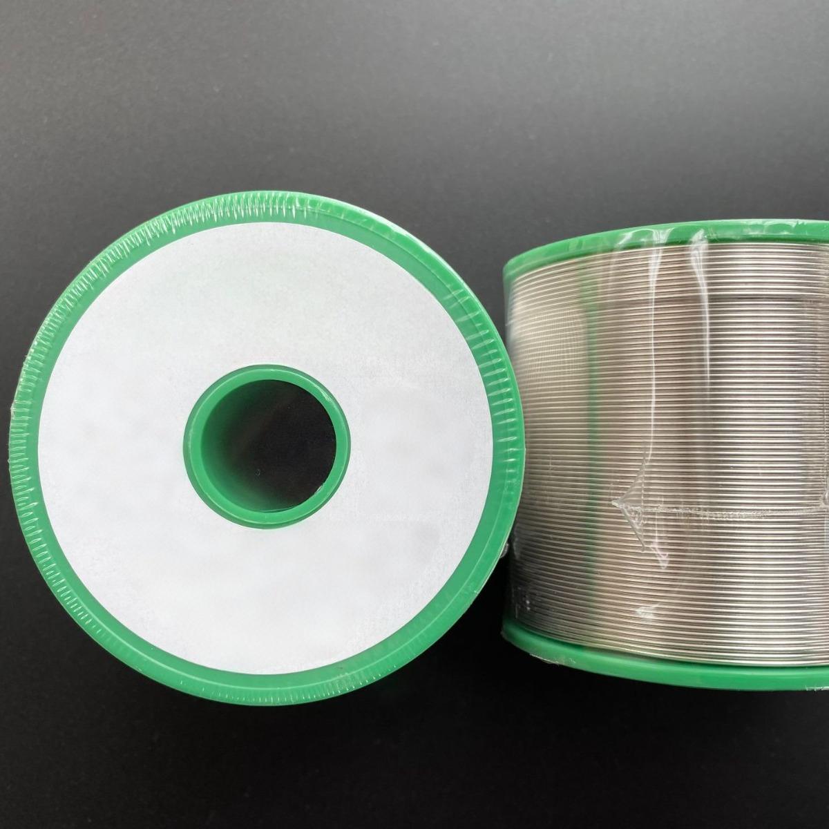
Need high-quality solder lead free? We offer RoHS certified lead free solder, engineered for all PCB through-hole and surface mount soldering processes with strong joint strength.
What is lead-free solder?
Lead-free solder is a solder alloy made without added lead. It was developed to reduce health and environmental risks linked to traditional leaded solder. In electronics manufacturing, it is now the default option for SMT and PCBA work across many markets.
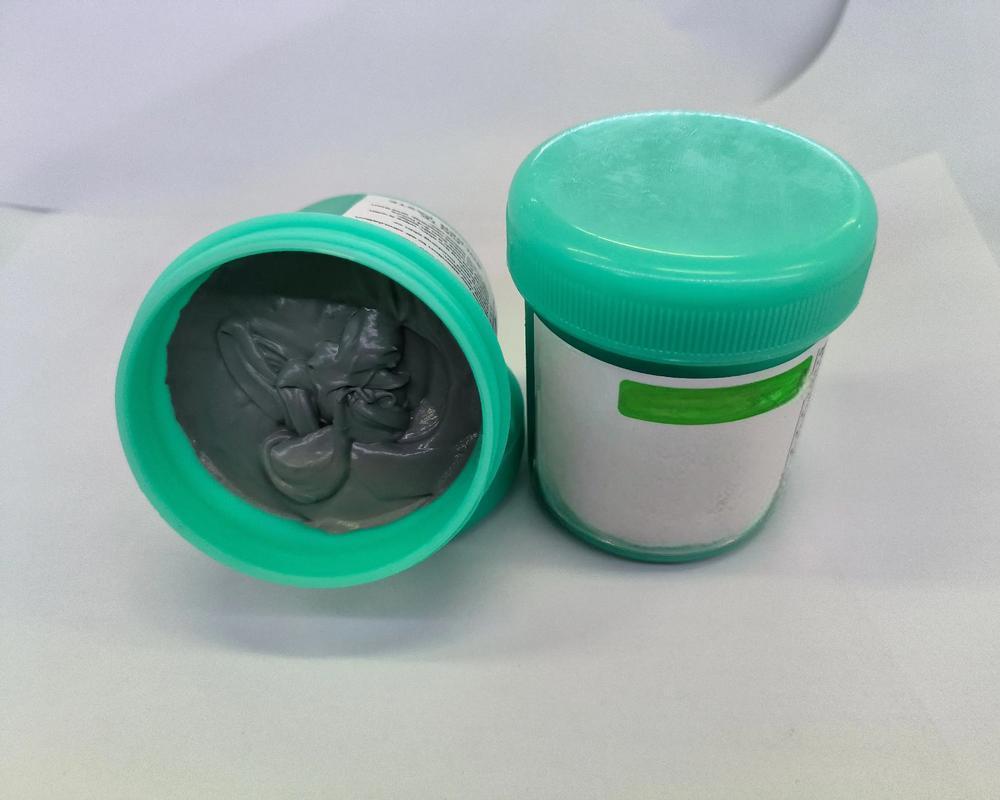
Most lead-free solder material is based on tin. Tin forms the backbone of the alloy. Other metals are added to improve strength, wetting, and durability. These metals often include silver, copper, bismuth, or small amounts of nickel.
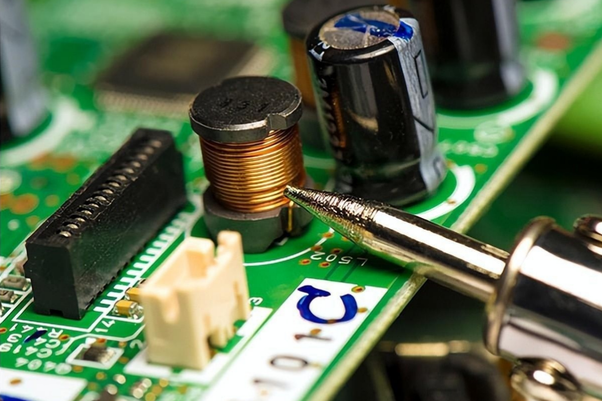
In practical use, solder lead free behaves a little differently from older leaded alloys. It melts at a higher temperature. It also forms joints with a different surface look. The joints may appear slightly dull or grainy.
For SMT lines, lead-free solder paste is used to print onto pads before component placement. During reflow, the paste melts and forms joints. For manual work or selective soldering, lead free solder wire is often used. The same alloy rules apply, but the form factor changes.
How to choose solder lead free?
Choosing the right solder lead free option starts with understanding your process. Not all assemblies are the same. Board design, component type, and thermal limits matter.
The first step is to look at the alloy family. The most common choice is SAC alloy. SAC stands for tin, silver, and copper. SAC305 is widely used in SMT and PCBA lines. It balances strength, cost, and reliability well.
Next, consider the melting point solder lead free alloys provide. Lead-free solder melting point is usually higher than leaded solder. This affects reflow profiles and hand soldering settings. Boards with heat-sensitive parts may need a lower-melt alloy with bismuth added.
You should also think about the solder form.
Lead free solder paste for SMT printing and reflow
Lead free solder wire for hand soldering and repair
Bar solder for wave or selective soldering
Each form must match the equipment used on the line.
Flux type is another key factor. Flux helps cleaning and wetting. No-clean flux is popular in modern factories. Water-soluble flux is used when cleaning is planned.
Why use solder lead free?
The strongest reason to use solder lead free is safety. Lead is toxic. Removing it reduces risk to workers and users.
Environmental protection is another major driver. Electronics waste is a growing issue. Lead-free solder lowers the impact when products reach the end of life. It supports cleaner recycling and disposal.
Compliance is also critical. Many markets require lead-free materials. RoHS rules limit lead content in electronics. Using lead-free solder helps products enter global markets without legal barriers.
Performance has improved over time. Early lead-free alloys had limits. Today, advanced formulations deliver strong joints. With the right profile, reliability is high in SMT and PCBA use.
At EBest Circuit (Best Technology), lead-free soldering is part of standard production. Our SMT lines are tuned for stable lead free solder temp control. This ensures consistent joints and long service life for assemblies.
What are the disadvantages of lead-free solder?
Lead-free solder does bring some challenges. The most known issue is higher process temperature. Lead free solder temperature during reflow is higher than leaded solder. This adds stress to boards and parts.
Wetting speed can be slower. The solder may take more time to flow across pads. This requires careful profile tuning and good flux selection.
Another concern is cost. Some alloys include silver. Silver raises material cost. However, the price gap has narrowed over time.
Lead-free joints may also look different. They are less shiny. This can confuse new operators. Training helps teams understand what good joints look like.
Despite these points, most disadvantages are manageable. Modern equipment handles higher heat well. Proper design reduces risk. Process control solves most issues before they appear.
Is lead-free solder still toxic?
Lead-free solder is safer than leaded solder. It removes a major toxic element. However, it is not completely harmless.
The metals used, such as tin, silver, and copper, are far less dangerous than lead. In solid form, they pose very low risk. During soldering, fumes come mainly from flux, not metal.
Good ventilation is still needed. Fume extraction protects workers from flux vapors. This applies to both lead-free and leaded solder.
How can I tell if my solder is lead free?
Identifying lead-free solder is usually simple. Most products are clearly labeled. Packaging often states lead-free solder or lead-free solder wire on the label.
There are a few common signs:
Alloy codes like SAC305 or Sn96.5Ag3Cu0.5
RoHS or lead-free symbols on packaging
Higher melting behavior during use
If labeling is missing, material testing can confirm composition. XRF testing is widely used in factories. It quickly checks metal content without damage.
At EBest Circuit (Best Technology), incoming solder materials are verified. This ensures full compliance and stable production from the first print to final inspection.
What is RoHS for solder lead free?
RoHS stands for Restriction of Hazardous Substances. It is a regulation that limits certain materials in electronics. Lead is one of the restricted substances.
For solder lead free compliance, RoHS sets a maximum lead content. The limit is very low. Most lead-free solders are well below this level.
RoHS applies to many product categories. Consumer electronics, industrial controls, and medical devices often fall under its scope.
RoHS is not just a label. It requires traceability and proof. Suppliers must provide declarations and test reports.
EBest Circuit (Best Technology) works with RoHS-compliant solder suppliers. We maintain records for each batch.
Which solder lead free fits PCBA?
PCBA work covers many applications. The best solder lead free choice depends on use case. General SMT assembly often uses SAC305. It offers strong joints and wide acceptance.
For boards with fine-pitch parts, solder paste with good slump resistance is key. This supports clean printing and reduces bridging.
High-reliability products may use modified alloys. Small additions of nickel or bismuth can improve joint life. Automotive and industrial boards often benefit from these options.
Thermal limits matter. If components cannot handle high heat, a lower melting lead-free alloy may be chosen. This protects parts while staying compliant.
EBest Circuit (Best Technology) evaluates each project. We match solder type to board design and product needs. This approach improves yield and long-term stability.
How to use solder lead free for SMT?
Using solder lead free for SMT requires control and consistency. The process is well known but must be followed closely.
First, solder paste storage is critical. Paste must be kept cold and sealed. Before use, it should reach room temperature naturally.
Stencil printing comes next. Proper stencil thickness and aperture design ensure even paste volume. Lead-free solder paste is sensitive to print quality.
Component placement should be accurate. Lead-free solder does not self-align as easily as leaded solder. Placement precision matters more.
Reflow profiling is the heart of the process. Lead free solder temp profiles usually include:
A controlled preheat stage
A soak zone for flux activation
A peak temperature above melting point
A smooth cooling stage
The peak temperature must be high enough to fully melt the alloy. At the same time, it should stay within component limits.
Inspection follows reflow. Visual checks and AOI confirm joint shape and coverage. Acceptable joints may look matte. This is normal for lead-free solder.
What affects solder lead free performance?
Many factors influence solder lead free results. Material choice is only one part. Process control plays a major role.
Board finish affects wetting. ENIG, OSP, and immersion silver each interact differently with lead-free solder. Selecting the right finish helps joint quality.
Component plating also matters. Tin-based finishes work well. Mixed finishes can cause uneven wetting.
Thermal profile accuracy is critical. Small changes in lead free solder temperature can change joint quality. Regular profile checks keep results stable.
Flux chemistry impacts residue and wetting speed. Choosing the right flux reduces defects and cleaning needs.
Environmental control helps too. Humidity and cleanliness affect paste behavior. Stable factory conditions support consistent output.
Conclusion:
Lead-free solder has become the standard for SMT and PCBA manufacturing. It improves safety, supports global compliance, and delivers strong performance when used correctly.
For professional PCBA and SMT services using proven lead-free soldering processes, contact EBest Circuit (Best Technology) at sales@bestpcbs.com
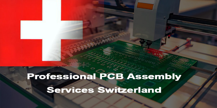
PCB assembly services Switzerland specialize in high-precision, compliant production for medical, aerospace, and industrial sectors, using advanced SMT and THT equipment paired with rigorous quality checks. These PCB assembly services Switzerland consistently meet global industry standards, addressing the specific needs of businesses requiring durable, high-performance electronic components.
Stringent quality compliance: Adheres to ISO 9001:2015, ISO 13485:2016, and IPC-A-610 Class 3 standards, critical for high-reliability applications.
Precision manufacturing capabilities: Master advanced processes like MSAP, supporting ultra-fine line/space down to 10μm and HDI boards with 30μm line widths.
Localized supply chain efficiency: Proximity to European component suppliers reduces lead times and minimizes logistics disruptions.
Zero-defect delivery record: Consistent compliance with EEMUA quality standards, ensuring minimal rework and project delays.
Flexibility for small to large batches: Adapts to low-volume prototypes and high-volume production without compromising cost or speed.
Specialization in medical and industrial sectors: Deep expertise in assembling PCBA for devices requiring extreme temperature resistance (-55°C to 125°C) and biocompatibility.
End-to-end traceability: Full material and process tracking via MES systems, ensuring accountability and easy compliance audits.
Pain Points of PCB Assembly Services Switzerland
Component shortage and unstable lead times: Global chip shortages and international logistics delays often disrupt material sourcing for time-sensitive projects.
Counterfeit or refurbished component risks: Unverified suppliers may provide substandard parts, leading to batch failures and compliance violations.
High cost for small-batch production: Tooling, setup, and testing costs are disproportionately high for low-volume orders, increasing per-unit expenses.
Strict compliance and certification barriers: Meeting ISO 13485, RoHS, and IPC standards requires significant investment in processes and training.
Complex process control for high-density boards: HDI and BGA assemblies demand precise equipment calibration, leading to higher defect rates without proper expertise.
Inadequate testing coverage: Certain board areas (e.g., component bottoms) are hard to inspect via AOI, leading to missed defects.
Delayed delivery due to design mismatches: Lack of DFM reviews leads to design changes mid-production, extending lead times and increasing costs.
One Stop Switzerland PCBA Service: Solving Supply Chain Delays Problems
Our one-stop Switzerland PCBA service eliminates supply chain delays primarily through integrated resource synergy and streamlined supply chain management, a core strength distinguishing our services. We have established a stable cooperative network with 15+ globally verified component suppliers and built a professional intelligent component warehousing center, stocking core electronic components commonly used in medical and industrial fields. This integrated resource layout avoids risks of component shortages and long international logistics cycles, shortening component sourcing lead time from 4-6 weeks to 3-5 days and fundamentally solving delays caused by material acquisition difficulties.
The comprehensiveness of our one-stop service ensures smooth supply chain operation by integrating pre-production DFM review, component verification, precision assembly, full-process testing, and timely delivery into a seamless process. We conduct professional DFM analysis before production to identify design mismatches that may cause mid-production modifications, avoiding delays from rework. Simultaneously, we utilize MES intelligent management systems for real-time tracking of production and logistics, dynamically adjusting production schedules based on order urgency to ensure each link is closely connected, enabling reliable on-time delivery even for urgent orders.
Why Choose EBest(Best Technology) for PCB Assembly Services Switzerland?
5-Year Quality Warranty: We provide a 5-year quality warranty for all our PCB assembly services Switzerland, covering manufacturing defects, soldering issues, and assembly-related component failures, offering free repair or replacement to minimize your post-delivery risks and ensure long-term product reliability.
Advanced MES Tracking System: Our advanced MES (Manufacturing Execution System) enables real-time tracking of the entire production process, from material incoming to final delivery, supporting end-to-end traceability of materials, processes and test data for easy compliance audits and production progress inquiry.
Strict Multi-Level Quality Inspection: We implement three-level quality inspection (incoming material inspection, in-process inspection, final inspection) using AOI, X-ray and functional testing equipment, ensuring a first-pass yield of 99.8% and eliminating defective products before delivery.
Rapid Prototype Turnaround: We offer fast prototype assembly with a 24-48 hour turnaround time and small-batch production delivery within 3-5 days, accelerating your product development cycle and helping you launch products to market faster.
Customized Assembly Solutions: We tailor assembly processes to your unique project needs, including ultra-miniaturized components (01005), high-temperature resistant PCBA (-55°C to 125°C) and HDI boards with 10μm line/space, adapting to diverse industry requirements.
Full Compliance Certifications: We hold ISO 9001:2015, ISO 13485:2016, and IPC-A-610 Class 3 certifications, fully meeting the strict compliance requirements of medical, industrial and high-reliability electronic fields in Switzerland.
Transparent Pricing & No Hidden Fees: We provide detailed, itemized quotes upfront, with zero setup fees for orders over 100 units, ensuring you have clear cost control without any unexpected additional charges.
Comprehensive Testing Services: We offer one-stop testing services including ICT, FCT, functional testing and reliability testing, verifying every PCB assembly’s performance and durability to avoid post-delivery failures.
Global Verified Supplier Network: We cooperate with 15+ globally verified component suppliers and operate an intelligent warehousing center, ensuring stable material supply and shortening sourcing lead times to 3-5 days.
24/7 Dedicated Project Support: Our professional team is available 24 hours a day, 7 days a week to respond to your inquiries, update project progress and resolve any assembly-related issues promptly.
Types of PCB Assembly Services Switzerland We Offered
PCB Manufacturing Types
Rigid/Flexible/Rigid-Flex Boards: Supports sizes ranging from 50mm to 700mm × 460mm, suitable for industrial equipment and wearable electronics.
Custom Shaped Circuit Boards: Provides cutting of circular, rectangular, and non-transparent special-shaped PCBs to meet the needs of space-constrained applications such as medical equipment.
Production Service Modes
Small Batch Rapid Prototyping: Equipped with a real-time MES scheduling system, responding to production line bottlenecks within 1 hour to ensure timely delivery of urgent orders.
Medium to Large Volume Manufacturing: Coordinates component procurement through a local Swiss supply chain network (Zurich/Biel) to reduce logistics delay risks.
Value-Added Services
Design Engineering Support: Collaborates with institutions such as CSEM to provide signal integrity optimization, compatible with high-frequency applications in automotive electronics.
Full-Process Quality Monitoring: 100% production data traceability, compliant with ISO and CE certification standards.
Mechatronics Assembly: Extends to the integrated assembly of precision components (such as printer heating units).
Our Switzerland PCBA Capabilities
Item
Capabilities
Placer Speed
13,200,000 chips/day
Bare Board Size
0.2 x 0.2 inches – 20 x 20 inches/ 22*47.5 inches
Minimum SMD Component
01005
Minimum BGA Pitch
0.25mm
Maximum Components
50*150mm
Assembly Type
SMT, THT, Mixed assembly
Component Package
Reels, Cut Tape, Tube, Tray, Loose Parts
Lead Time
1 – 5 days
Case Studies of Medical PCB Assembly Services Switzerland
Project Background: A Swiss medical device company sought a trusted partner for assembling PCBA for their new neurostimulator. Dissatisfied with their previous provider’s inconsistent quality and missed deadlines, they needed a reliable PCB assembly services Switzerland provider meeting strict medical device manufacturing standards.
Project Requirements: Key requirements included a 12-layer rigid-flex PCB assembly, ISO 13485:2016 compliance, 99.8% first-pass yield, 14-day delivery, 30μm line/space for high-density components, and FDA certification compatibility.
Project Challenges: Critical challenges included: ±100μm layer-to-layer alignment error causing intermittent signal failure (risking FDA failure); difficult placement of small 0201 components (prone to soldering defects); and strict biocompatibility requirements for all materials.
Our Solutions: Our solutions addressed these challenges: optical alignment closed-loop control reduced alignment error to ±50μm; high-precision SMT machines ensured accurate 0201 component placement; we sourced biocompatible, RoHS-compliant materials with MES traceability; and pre-production DFM reviews prevented potential issues.
Output Results: Exceptional results: 99.9% first-pass yield, 500 units delivered 2 days early, consistent ±45μm alignment error, zero FDA pre-certification non-conformities, and a 0.05% failure rate during 6-month field trials, demonstrating our reliable PCB assembly services Switzerland.
FAQs of PCB Assembly in Switzerland
Q1: How can I ensure components used in Swiss PCBA are not counterfeit? A1: Partner with suppliers that provide full material traceability (batch IDs, certificates of conformity) and conduct incoming inspections using X-ray and optical testing. We verify all components against IPC standards and maintain a list of 15+ verified local suppliers to eliminate counterfeit risks.
Q2: What is the typical lead time for PCB assembly services Switzerland? A2: Lead times vary by order size: prototypes (24-48 hours), small batches (10-100 units: 3-5 days), medium batches (100-1,000 units: 7-10 days), and large batches (1,000+ units: 10-14 days). Local component warehousing can reduce lead times by 30-40%.
Q3: Is it cost-effective to use small-batch PCB assembly in Switzerland? A3: Yes, with our zero setup fees for orders over 100 units and optimized production processes, we reduce per-unit costs by 25% for small batches. We also offer flexible pricing for repeat small-batch orders to further lower costs.
Q4: How do I ensure my PCBA meets Swiss medical device compliance standards? A4: Work with a provider certified to ISO 13485:2016 and experienced in medical PCBA. We conduct pre-production compliance reviews, use FDA-approved materials, maintain end-to-end traceability, and provide documentation required for CE and FDA certifications.
Q5: What should I do if my PCB design has DFM issues for Swiss assembly? A5: Request a free DFM review before production. Our team identifies design mismatches (e.g., component spacing, pad size) within 24 hours and provides actionable adjustments to optimize for Swiss assembly processes, reducing rework and delays.
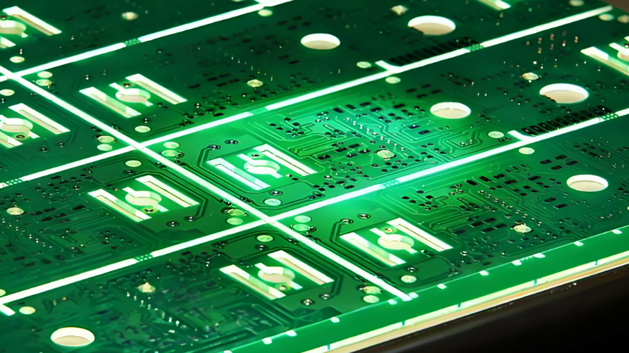
Why PCB is green? Most printed circuit boards appear green because of the solder mask, a protective polymer coating applied over copper traces. This layer prevents oxidation, avoids solder bridging during assembly, and improves long-term durability. Historically, manufacturers standardized on green because early solder mask chemistry produced the most stable color in that shade. Over decades, fabrication lines, inspection systems, and operator training all evolved around green boards, reinforcing it as the default option.
Another practical reason is visibility. Green provides balanced contrast between copper pads, silkscreen markings, and components. For engineers reviewing assemblies under microscopes or AOI cameras, this contrast reduces eye fatigue and improves defect detection.
Why Are Most PCBs Green Instead of Red, Blue or Black?
Green solder mask delivers a combination of process stability, inspection clarity, and cost efficiency. Alternative colors exist, but they introduce certain trade-offs:
Dark colors like black absorb more light, making scratches or solder bridges harder to detect.
White boards reflect excessive light, which may interfere with automated inspection.
Bright colors sometimes require extra pigment loading, which slightly complicates coating uniformity.
Because fabrication lines have optimized exposure parameters, curing temperatures, and AOI algorithms around green, it remains the safest production choice for high-volume manufacturing.
What Is the Green Part of a Circuit Board Made Of?
The green layer is typically an epoxy-based liquid photoimageable (LPI) solder mask. It consists of:
Epoxy resin matrix
Photoinitiators for UV curing
Pigments that produce the green coloration
Fillers for mechanical strength and thermal stability
During fabrication, the mask is applied as a liquid coating, exposed through artwork, and then chemically developed to reveal pads. The resulting film protects copper traces from contamination while maintaining insulation between conductors.
Does Green PCB Color Improve Electrical Performance or Reliability?
Color alone does not alter impedance, signal speed, or electrical conductivity. Those characteristics depend on stackup design, copper geometry, and dielectric materials.
However, green boards often appear more reliable because:
Stable processing reduces solder mask defects
Easier inspection improves yield rates
Mature chemistry lowers variation between batches
In practice, reliability benefits come from manufacturing consistency rather than color physics.
Why Do Engineers Prefer Green PCB for AOI and Inspection Accuracy?
Automated Optical Inspection systems rely on controlled lighting and contrast recognition. Green solder mask reflects light in a balanced spectrum that helps cameras differentiate between pads, traces, and silkscreen markings.
Benefits for inspection include:
Reduced glare compared to white surfaces
Higher edge contrast than dark colors
Stable color recognition for machine vision algorithms
Human operators also find green less visually exhausting during long inspection sessions, which further improves quality control.
Is Green PCB Cheaper Than Other PCB Colors in Mass Production?
Yes — in most cases. The price difference comes from process optimization rather than pigment cost.
Why green often costs less:
High demand lowers material procurement costs
Default exposure and curing settings reduce setup time
Fewer inspection challenges lower yield risk
For large production runs, alternative colors may only increase cost slightly, but for prototypes the difference can be noticeable.
Why Did Green Become the Industry Standard Historically?
Early PCB manufacturing in the 1970s and 1980s used epoxy-based solder masks that naturally appeared green due to pigment chemistry. At the time:
Green dyes provided the best UV stability.
Alternative pigments were less resistant to heat and solvents.
Military and industrial standards documented green as the reference color.
Once assembly houses invested in equipment calibrated for green boards, the ecosystem reinforced itself. Even today, many legacy production lines maintain settings optimized for that traditional color.
When Should You Choose Black, White or Blue PCB?
Modern fabrication supports many solder mask colors. Each serves different purposes:
Black PCB — popular for consumer electronics aesthetics or stealth designs.
White PCB — often used in LED lighting to improve light reflection.
Blue PCB — chosen for branding or prototype differentiation.
Red PCB — common in development kits and educational hardware.
Color selection should be based on inspection needs, thermal considerations, and product appearance rather than performance myths.
Green PCB vs Black PCB — Which One Is Better for High-Density Designs?
High-density interconnect (HDI) designs demand precise inspection and minimal defects. Green boards usually provide clearer contrast for microvias, fine-pitch components, and solder joints.
Black PCBs can look visually premium, but they present challenges:
Lower visibility for hairline scratches
Harder optical inspection
Increased glare under certain lighting angles
For extremely dense layouts, many engineering teams still favor green for manufacturing reliability.
Does PCB Color Affect Heat Dissipation or Thermal Performance?
Color itself has minimal influence on thermal conductivity. Heat transfer is governed by:
Copper thickness
Thermal vias
Substrate material (FR-4, aluminum, ceramic, etc.)
Dark colors may absorb more radiant heat in open environments, but inside electronic assemblies this effect is negligible compared with structural design choices.
Why Do Many Prototype PCBs Still Default to Green Color Today?
Prototype fabrication emphasizes speed and predictability. Green boards allow manufacturers to:
Use default process parameters without additional setup
Maintain fast turnaround times
Reduce risk during early design validation
Because engineering teams often prioritize quick iteration, green remains the standard option for prototypes.
Are Custom Color PCBs More Expensive or Harder to Manufacture?
Custom colors are generally feasible, but several factors may affect cost:
Extra quality checks to ensure color uniformity
Slightly different curing behavior depending on pigment type
Potentially longer lead times for non-standard materials
In high volumes, price differences become smaller, but for quick-turn orders, green usually stays the most economical choice.
FAQs
Does green solder mask mean a PCB is higher quality?
Not necessarily. Quality depends on fabrication control, materials, and design rules rather than color.
Can I mix PCB colors within one project?
Yes. Some designers use different colors to identify board revisions or functional modules during testing.
Is black PCB more conductive or faster?
No. Electrical performance is determined by copper geometry and dielectric properties, not by solder mask color.
Why do some premium consumer devices use black boards?
Mainly for aesthetics and branding. Engineering teams often accept inspection trade-offs to achieve a distinctive visual style.
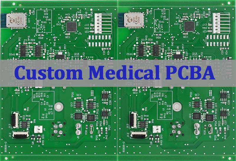
Custom Medical PCBA plays a critical role in modern healthcare electronics, where PCB reliability, PCBA traceability, and regulatory compliance are non-negotiable. From patient monitoring systems to diagnostic imaging equipment, medical devices demand precise SMT PCB assembly processes supported by strict quality systems such as ISO13485 and IPC Class 3 standards. This guide explains how engineers and procurement teams can evaluate suppliers, understand design requirements, and ensure long-term stability when developing custom PCBA for regulated medical applications.
Unlike consumer electronics, medical PCBA projects involve higher documentation standards, tighter process control, and extended product life cycles. EBest Circuit (Best Technology) delivers high-reliability custom medical PCBA solutions in line with ISO 13485 standards, supporting medical and high-precision electronic applications with strict quality control and full traceability. By working closely with customers, the engineering team helps clients have a better picture of manufacturability risks while giving them easy access to professional DFM feedback and global supply chain resources. This collaborative approach provides a strong head start during product development and helps heighten overall reliability, efficiency, and compliance from prototype stages through mass production. For more information or inquiries, please contact us via the form on our Contact page.
What Defines A Reliable Custom Medical PCBA Manufacturer For Regulated Healthcare Devices?
A dependable manufacturer must demonstrate more than basic SMT capability. Medical electronics require strict process discipline and full lifecycle management.
Key characteristics include:
ISO13485-certified quality management systems
Full traceability for components and manufacturing batches
Controlled ESD environments and clean assembly conditions
Advanced inspection technologies such as AOI, AXI, and functional testing
Reliability is closely linked to process consistency. A reliable partner maintains standardized work instructions, validated reflow profiles, and strict material control procedures. These elements reduce the risk of latent defects that could compromise patient safety.
In addition, experienced manufacturers support early-stage DFM reviews. By identifying potential issues such as pad geometry or thermal imbalance, they help engineers prevent costly redesigns later in the project lifecycle.
What Design Rules Should Engineers Follow When Building A Custom Medical PCBA For Diagnostic Devices?
Designing PCBA for diagnostic equipment requires balancing electrical performance with regulatory constraints. Engineers typically follow conservative design principles to ensure long-term stability.
Important design considerations include:
Using medical-grade components with long lifecycle availability
Maintaining adequate creepage and clearance distances
Implementing redundant grounding paths for noise-sensitive circuits
Selecting high-reliability surface finishes such as ENIG or ENEPIG
Thermal management is another major factor. Diagnostic systems often run continuously, which increases the risk of thermal fatigue. Designers must optimize copper distribution, via structures, and component spacing to maintain stable operating temperatures.
Documentation also forms part of the design process. Detailed fabrication drawings, BOM traceability, and revision control are essential to comply with regulatory audits.
How Does PCB Customized Immersion Gold Bare PCBA Board For Medical Equipment Enhance Long-Term Reliability?
Immersion gold surface finishes, commonly known as ENIG, are widely used in medical electronics due to their excellent corrosion resistance and stable solderability. A pcb customized immersion gold bare pcba board for medical equipment helps maintain consistent electrical performance over extended product lifetimes.
Advantages include:
Flat surface suitable for fine-pitch components and BGAs
Strong resistance to oxidation during storage
Improved contact reliability for connectors and test points
For devices exposed to repeated sterilization or harsh environments, ENIG reduces the risk of surface degradation. The nickel layer acts as a diffusion barrier, while the gold layer provides stable conductivity.
However, process control is critical. Improper plating thickness or poor bath management can lead to black pad issues. Therefore, manufacturers must maintain strict chemical monitoring and inspection routines.
What Testing And Validation Steps Are Required For Custom ISO13485 Medical PCBA Before Mass Production?
Medical PCBA projects typically undergo extensive validation before entering full production. These procedures ensure compliance with regulatory requirements and confirm product reliability.
Common testing stages include:
Design Verification Testing (DVT) to confirm electrical performance
Process Qualification to validate SMT parameters
Functional testing under simulated operating conditions
Environmental stress screening such as thermal cycling
Manufacturers following ISO13485 standards also maintain structured documentation, including IQ/OQ/PQ reports and traceability records. These documents support regulatory submissions and provide evidence of process consistency.
Early testing reduces the risk of field failures and helps identify potential design weaknesses before mass production begins.
How To Evaluate A Supplier Offering Custom ISO13485 Medical PCBA For USA Medical Projects?
When sourcing a custom ISO 13485 medical pcba partner, engineers should assess both technical capability and regulatory readiness.
Evaluation criteria may include:
Experience with FDA-regulated products
Availability of in-house engineering support
Capability to handle multilayer and HDI PCB structures
Traceability systems such as MES or barcode tracking
Communication is equally important. A responsive engineering team can quickly address design changes, component shortages, or compliance questions, ensuring smoother project execution.
Additionally, suppliers should provide transparent documentation processes. Clear reporting builds trust and simplifies audits during product certification stages.
When Should You Consider China Custom-Made ISO13485 Multilayer Medical Electronics Interface PCBA?
Global supply chains often combine USA design expertise with advanced manufacturing resources from overseas. Choosing China custom-made ISO13485 multilayer medical electronics interface pcba may be beneficial in several scenarios.
Advanced assembly processes such as microvia HDI or fine-pitch placement
Collaborating with experienced international manufacturers allows OEMs to access mature supply chains and specialized equipment. However, successful collaboration depends on strong quality management and transparent communication channels.
Many USA-based companies adopt a hybrid model, where early prototyping and design validation occur locally while mass production leverages global manufacturing capacity.
In closing, custom medical PCBA manufacturing requires a careful balance between engineering precision and regulatory compliance. From design rules to testing validation and supply chain selection, every stage plays a role in ensuring safe and reliable medical devices. By working with experienced manufacturers that understand ISO 13485 processes and advanced PCB assembly techniques, healthcare companies can accelerate product development while maintaining strict quality standards.
Whether you are developing diagnostic PCBA equipment, wearable medical PCBA electronics, or advanced imaging PCBA systems, choosing the right manufacturing custom ISO 13485 medical PCBA partner helps reduce risk, improve product longevity, and ensure compliance with global healthcare regulations. Feel free to reach out to us at sales@bestpcbs.com for any technical questions or project discussions.
FAQs About Custom Medical PCBA
Do Custom Medical PCBA Suppliers Need To Hold ISO13485 Certification?
Yes. ISO13485 certification demonstrates that a manufacturer follows structured quality management processes tailored for medical device production. While additional standards may apply depending on the product category, ISO13485 is widely considered the baseline requirement for regulated healthcare electronics.
What Documentation Should Engineers Request From A Custom Medical PCBA Supplier Before Production?
Engineers should request process flow charts, inspection reports, material certifications, and traceability records. Documentation such as DFM analysis, validation reports, and quality control plans helps ensure that the supplier meets regulatory expectations.
How Do Engineers Verify Whether A Custom Medical PCBA Supplier Is Truly Compliant?
Compliance can be verified through on-site audits, certification checks, and reviewing process documentation. Engineers often evaluate whether the supplier maintains consistent testing procedures, documented work instructions, and controlled production environments aligned with ISO13485 standards.
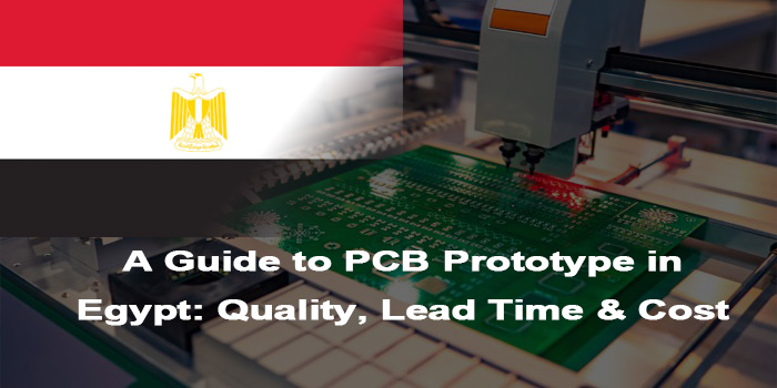
PCB prototype in Egypt has become a reliable option for fast, cost-effective small-batch circuit board sampling, with local manufacturers offering diverse capabilities to meet global standards. Most Egyptian facilities focus on precision and efficiency, making PCB prototype in Egypt suitable for various electronic projects that require quick design verification and reliable performance without excessive lead times or costs.
Strategic location in Alexandria, export-ready service
Single/double-layer PCB, impedance control (optional)
Standard: 4-8 days
Where Can I Find Reliable PCB Prototype Services in Egypt?
To efficiently find reliablePCB prototype services in Egypt, combine targeted channel selection and preliminary verification based on your project’s scale, budget, and quality needs. Practical approaches include leveraging both offline/online channels and applying professional verification methods to identify trustworthy local providers.
Local Industrial Clusters: Focus on industrial zones in Cairo and Alexandria, where most reliable PCB prototype manufacturers (such as Pyramid Electronics, Ronex Misr) are concentrated. You can visit factories on-site for consultations, check production equipment, and verify sample quality in person.
International B2B Platforms: Use well-known platforms like Alibaba and MFG.com to find verified Egyptian PCB prototype suppliers. These platforms provide detailed factory profiles, process capabilities, customer reviews, and transaction guarantees for easy comparison and screening.
Egyptian Industry Associations: Contact the Egyptian Electronic Manufacturers Association (EEMA) to obtain a directory of certified PCB prototype facilities. Members of the association usually comply with international quality standards and have standardized production processes.
Direct Factory Contact: Reach out to leading manufacturers directly via their official websites, such as PEModule (a cost-effective option supporting startup projects) and SMT Egypt. You can get customized quotes, technical support, and real-time updates on prototype progress.
Local Electronic Exhibitions: Attend electronic industry exhibitions held in Cairo regularly, where Egyptian PCB manufacturers (including UETPCB Egypt and Hitec Pioneers) showcase their prototype capabilities. It’s a good opportunity to communicate face-to-face and establish cooperative relationships.
Customer Referrals: Consult peers or partners who have previously cooperated with Egyptian PCB manufacturers. Their real cooperation experiences can help you screen reliable suppliers and avoid potential risks, especially for small-batch prototype orders.
Third-Party Quality Certification Platforms: Search for Egyptian PCB prototype manufacturers certified by UL, TUV, or other international organizations. These certifications ensure that manufacturers have strict quality control systems and can produce prototypes meeting global standards.
Electronic Component Suppliers: Cooperate with local electronic component suppliers in Egypt. They often have long-term cooperative relationships with PCB prototype factories and can recommend reliable manufacturers that match your project requirements, such as Sama Marketing which provides component supply and PCB prototyping.
Which Quality Standards do PCB Prototype in Egypt Meet?
IPC Core Standards: Most Egyptian PCB prototype factories strictly follow IPC-A-600 (PCB Appearance Standard) and IPC-6012 (Rigid PCB Performance Standard). These standards define acceptable appearance defects, dimensional tolerances, and electrical performance requirements, ensuring PCB prototype in Egypt meets basic to high-grade quality for reliable project design verification.
IPC Soldering Standards: In addition to core standards, leading manufacturers comply with IPC-J-STD-001 (Requirements for Soldered Electrical and Electronic Assemblies), ensuring consistent solder joint quality, which is critical for the reliability of PCB prototypes during assembly and use.
ISO Certifications: Key Egyptian PCB prototyping facilities hold ISO 9001 (Quality Management System) and ISO 14001 (Environmental Management System) certifications. These certifications standardize production workflows, quality control processes, and environmental practices, guaranteeing consistent prototype quality across batches.
RoHS 2.0 Compliance: Lead-free manufacturing processes are universally adopted by Egyptian PCB factories, fully meeting EU RoHS 2.0 requirements. This restricts hazardous substances (lead, cadmium, mercury, etc.) in prototypes, making PCB prototype in Egypt suitable for global markets, including the EU and North America.
UL Flame Retardant Standards: Reputable manufacturers (such as UETPCB Egypt and Egyptian Electronic Technology) comply with UL 94 flame retardant standards, using FR-4 substrates with V-0 flame retardant grade to enhance the safety and durability of PCB prototypes.
Egyptian Local Compliance: All PCB prototypes produced in Egypt meet local regulations, including ESMA (Egyptian Telecommunication Regulatory Authority) certification and EOS 3000 industrial safety standards, ensuring seamless market access in Egypt and the MENA region.
How to Ensure the Quality of PCB Prototype in Egypt?
Verify Factory Certifications: Confirm Egyptian PCB prototype factories hold ISO 9001 (quality management) certification covering ≥95% of production processes, IPC certifications (IPC-A-600 Class 2 or Class 3, IPC-6012 for rigid PCBs), plus local ESMA 2020/12 compliance. Ask for quality control documents (production flowcharts, inspection checklists) that specify a first-article inspection pass rate of ≥99.5% to ensure standardized workflows.
Request Pre-Production Samples: For critical projects, request 1-2 pre-production samples to check key parameters: PCB thickness (tolerance ±0.1mm, high-precision models ±0.05mm), copper foil thickness (1oz=35μm±10%, 2oz=70μm±10%), surface finish (ENIG: Au≥0.05μm, Ni≥3μm; HASL: tin layer 20-50μm), and dimensional tolerances (board edge ±0.1mm, line width ±0.02mm), ensuring alignment with your design requirements.
Specify Quality Inspection Requirements: Require AOI (automated optical inspection) with ≥99.8% coverage for appearance defects (detecting minimum line width/spacing 0.05mm, false positive rate ≤0.3%) and flying probe testing with ≥99.5% test point coverage for electrical performance. This ensures detection of short circuits, open circuits, and poor via connectivity (≤1Ω conductivity abnormality) in PCB prototype in Egypt.
Clarify Material Specifications: Confirm high-quality substrates (e.g., FR-4 high-TG ≥170℃, Td≥300℃, dielectric constant εr=4.2±0.2 at 1GHz), specify copper thickness (1oz=35μm, 2oz=70μm, max 4oz=140μm) with ±10% tolerance, surface finish type, and line width/line spacing (minimum 0.1mm, tolerance ±0.02mm) in the order.
Confirm Production Process Control: Ask manufacturers to provide key process parameters: lamination (175±5℃, 350±50psi, 75±10 minutes), drilling precision (laser drilling ±0.02mm, mechanical drilling ±0.05mm), soldering temperature (reflow peak 245±5℃, 30-60 seconds holding time), and solder paste thickness (0.12-0.15mm, ±0.02mm tolerance) to ensure consistent prototype quality.
Establish Real-Time Communication: Maintain daily progress updates (before 10:00 AM local time) and require instant feedback (≤1 hour) for key production nodes (material preparation, drilling, testing). Set a ≤2-hour response time for design/process issues and ≤4-hour solution proposal to avoid quality deviations.
Clarify After-Sales Quality Guarantee: Confirm terms for rework/remanufacturing (completed within 3 business days for factory-caused defects) and a prototype pass rate guarantee of ≥99.8%. Specify that factory-caused defects (e.g., mismatched design, poor soldering) incur 0 additional costs, with delayed rework compensated at 0.5% of the order value per day, plus a 30-day quality warranty.
What is the Typical Lead Time for PCB Prototype in Egypt?
PCB Type
Layer Count
Typical Lead Time (Business Days)
Rigid PCB
1-2 layers
2-4
Rigid PCB
4-6 layers
5-7
Rigid PCB
8-10 layers
7-10
Rigid-Flex PCB
2-6 layers
8-12
High-Frequency PCB
2-6 layers
6-9
What Are the Typical Costs for PCB Prototyping Services in Egypt?
Costs for PCB prototype in Egypt vary by layer count, size, quantity and process, with transparent pricing for small batches. Single-sided prototypes (10 pieces, 100x100mm) start at $30-$50. Double-sided prototypes (10 pieces, 100x100mm) range from $45-$70. 4-layer prototypes (10 pieces, 100x100mm) cost $80-$120, while 6-layer prototypes (10 pieces, 100x100mm) are $130-$180. Special processes (ENIG surface finish, blind/buried vias, impedance control) add 20%-50% to the base cost. Smaller quantities (1-5 pieces) may have a 10%-15% premium, while quantities over 50 pieces often qualify for volume discounts.
Do Egyptian PCB Manufacturers Take Small-Batch PCB Prototype Orders?
Yes, most Egyptian PCB manufacturers accept small-batch PCB prototype orders. The majority of local facilities specialize in small to medium batches, with minimum order quantities (MOQ) as low as 1 piece for prototypes. This flexibility caters to projects that require design verification or small-scale testing without large production commitments. Tailored pricing options are often available for small batches to ensure cost-effectiveness while maintaining quality standards. Small-batch orders also benefit from the same lead time and quality checks as larger orders, making them a practical choice for quick project iterations.
Is Expedited Delivery Available for Egyptian PCB Prototypes?
Yes,expedited delivery is available for PCB prototype in Egypt, with most manufacturers offering accelerated turnaround options for urgent projects. Standard expedited lead time for single/double-sided prototypes is 24-48 hours, while 4-6 layer prototypes can be delivered in 3-4 business days. Expedited services typically add 30%-60% to the base cost, depending on the prototype complexity and urgency. Manufacturers prioritize expedited orders by allocating dedicated production resources and streamlining quality checks, ensuring speed without compromising performance. It is recommended to confirm expedited availability and pricing when placing the order, especially for prototypes with special process requirements.
FAQs of PCB Prototyping in Egypt
Q1: Why do PCB prototypes from Egypt sometimes have uneven circuit traces or inconsistent etching? A1: Uneven circuit traces and inconsistent etching in PCB prototypes often result from improper etching solution concentration, unstable temperature control, or uneven exposure during the photolithography process. Choose Egyptian manufacturers that control etching parameters strictly: etching solution concentration (FeCl3: 38-42 Baume), temperature (45±3℃), and etching time (60-90 seconds). Most local facilities use automated spray etching equipment with ±1℃ temperature precision and post-etching AOI inspection (≥99.8% coverage) to eliminate such issues.
Q2: Can Egyptian PCB manufacturers handle prototypes with fine lines and small vias? A2: Yes, most reliable Egyptian PCB prototyping facilities can produce prototypes with fine lines and small vias, a key capability of professional PCB sampling. Leading factories use high-precision laser drilling machines (drilling precision ±0.02mm) and advanced photolithography equipment, supporting minimum line width/line spacing of 0.08mm-0.1mm and minimum via diameter of 0.2mm. Post-production AOI and flying probe testing ensure fine line integrity and via connectivity, meeting IPC-A-600 Class 2 or Class 3 standards.
Q3: How to resolve PCB prototype warpage issues from Egyptian manufacturers? A3: Warpage is a common issue in PCB prototyping, usually caused by improper substrate selection, uneven lamination pressure, or inconsistent cooling. To resolve it, specify high-TG FR-4 substrates (TG≥170℃, Td≥300℃) and request manufacturers to use programmed lamination curves (175±5℃, 350±50psi, 75±10 minutes). Post-production annealing (120℃ for 2 hours) can correct minor warpage, ensuring prototypes meet IPC-A-600 Class 2 warpage requirements (≤0.75% of board length).
Q4: Do Egyptian PCB prototypes meet international PCB sampling quality standards? A4: Yes, all reliable Egyptian PCB prototyping manufacturers produce samples that comply with international PCB sampling standards, primarily IPC-A-600 (PCB Appearance Standard) and IPC-6012 (Rigid PCB Performance Standard). Prototypes meet strict specifications for dimensional tolerance (board edge ±0.1mm), copper thickness tolerance (±10%), surface finish uniformity (ENIG: Au≥0.05μm, Ni≥3μm), and via connectivity (≤1Ω). Manufacturers also provide AOI and flying probe test reports to verify compliance with global sampling standards.
Q5: What should I do if the delivered PCB prototype does not match my Gerber design specifications? A5: First, provide the manufacturer with your original Gerber files and design specifications (line width, aperture, layer stack-up, copper thickness) for detailed comparison. Reputable Egyptian facilities offer free DFM (Design for Manufacturability) checks before PCB prototyping to identify and resolve design conflicts in advance. If a mismatch occurs due to factory error (e.g., incorrect line width, wrong aperture size, layer misalignment), they will remanufacture the prototype within 3 business days at no additional cost. To avoid this, confirm the DFM review report and pre-production sample (if requested) before full prototype production.
Medical PCBA (Printed Circuit Board Assembly) forms the electronic heartbeat of modern medical equipment, from diagnostic monitors to life-sustaining implants. This article explores the specialized world of medical device electronics manufacturing, detailing the critical standards, design considerations, and supply chain strategies that ensure safety, reliability, and accelerated innovation.
Developing a new medical PCBA device is fraught with unique challenges. Do you struggle with these common hurdles?
Navigating complex regulatory compliance (e.g., ISO 13485, FDA) for electronics.
Achieving high reliability and longevity in critical, life-dependent applications.
Sourcing biocompatible and high-performance materials for specialized designs.
Managing extended lead times for multilayer medical PCBA production and components.
Validating design functionality and manufacturability early without slowing down.
An expert medical PCBA manufacturer addresses these points directly.
Providing ISO13485 medical PCBA certified manufacturing and comprehensive documentation support.
Implementing rigorous medical PCBA quality control and testing protocols for high-reliability medical PCBA.
Offering expertise in material selection for biocompatible medical PCBA and high-performance medical PCBA designs.
Delivering quick turn PCBA prototype medical device services to compress development cycles.
Offering best turnkey PCB and PCBA small-batch services for medical devices for seamless early-stage builds.
At EBest Circuit (Best Technology), we are a specialized medical devicePCBA supplier focused on medical PCBA design, custom medical PCBA prototypes, precision medical PCBA mass production, and medical PCBA testing. We have implemented an MES system at our factory. And we combine ISO 13485:2016 certified processes with rapid prototyping expertise to offer fast track PCBA medical device development, helping you transition from medical PCBA design to ISO 13485 medical PCBA customized product with fast speed. A warm welcome to contact us at sales@bestpcbs.com to discuss your OEM medical control PCBA assembly project.
What Is Medical PCBA?
Medical PCBA refers to the specialized process of assembling printed circuit boards for use in medical devices and equipment. This domain demands an extreme focus on precision, traceability, and reliability, as these electronic assemblies often perform critical diagnostic, monitoring, or therapeutic functions.
Unlike consumer electronics, medical PCBAs are characterized by:
Stringent Regulatory Compliance: Adherence to standards like ISO 13485 (Quality Management) and IEC 60601-1 (Safety) is non-negotiable.
Enhanced Reliability Requirements: Devices must perform flawlessly over long service lives, often in demanding environments.
Material Rigor: Use of high-Tg laminates, biocompatible coatings, and conformal coatings suitable for sterilization or bodily contact.
Comprehensive Traceability: Full documentation of components, materials, processes, and test results for each batch or unit.
Robust Testing Regimens: Subjecting assemblies to rigorous electrical, environmental, and functional tests beyond standard industrial practice.
In essence, medical PCBA is the foundation upon which safe, effective, and innovative healthcare technology is built, requiring a manufacturing partnership that prioritizes quality and compliance above all else.
How Does PCBA Medical Device Manufacturing Differ From Standard Industrial PCBA?
The manufacturing of PCBA for medical equipment operates under a fundamentally different paradigm than standard industrial assembly, primarily governed by risk management and patient safety. The key distinctions are systemic and profound.
Aspect
Standard Industrial PCBA
Medical Device PCBA Manufacturing
Governance Standard
ISO 9001 Quality System
ISO 13485 Risk-Based QMS
Primary Driver
Cost, Performance, Speed
Safety, Compliance, Reliability
Traceability
Lot-Level Tracking
Full Batch or Unit Traceability
Documentation
BOM, Gerber, Assembly Files
DHF, DMR, Controlled Records
Cleanliness Control
IPC-Based Handling
Strict Contamination Control
Failure Impact
Downtime, Financial Loss
Patient Risk, Regulatory Exposure
Testing & Validation
Sample Testing
100% Testing, IQ/OQ/PQ
Therefore, choosing a partner experienced in medical electronics PCBA is critical. They understand that every process—from medical PCBA fabrication to final inspection—is part of a controlled, documented system aimed at ensuring the highest possible outcome for patient health.
What Materials And Standards Are Required For High-Reliability PCB Medical Designs?
Creating a high-reliability medical PCBA starts with the foundational choices of materials and adherence to a strict hierarchy of standards. These choices directly impact the device’s performance, longevity, and regulatory acceptability.
Core Material Considerations:
PCB Laminates: High-Tg (Glass Transition Temperature) materials like FR-4 Tg170 or polyimide are standard for better thermal and mechanical stability during assembly and in-field use.
Surface Finishes: For PCB customized immersion gold bare PCBA board for medical equipment, Immersion Gold (ENIG) offers excellent planarity for fine-pitch components and reliable shelf life. Other options include Immersion Silver or hard gold for edge connectors.
Conformal Coatings: Biocompatible, moisture-resistant coatings (e.g., USP Class VI approved silicone or parylene) are often required for wearable medical PCBA or devices exposed to fluids.
Components: Use of automotive-grade or higher-specification components to ensure tolerance to stress and long-term availability.
Essential Standards Framework:
ISO 13485:2016: The cornerstone quality management standard for medical device manufacturing.
IEC 60601-1: The international standard for basic safety and essential performance of medical electrical equipment.
IPC-A-610 (Class 3): The highest acceptability standard for electronic assemblies, mandatory for critical applications.
ISO 14971: Application of risk management to medical devices.
FDA 21 CFR Part 820: Quality System Regulation for devices marketed in the United States.
EU MDR (2017/745): Regulatory framework for devices in the European Union.
A proficient custom ISO13485 medical PCBA partner guides this selection process, ensuring your medical PCB assembly meets all material and regulatory prerequisites for a successful submission.
Why Is Multilayer Medical PCBA Production Important For Advanced Diagnostic Systems?
Multilayer medical PCBA production is not just a technical choice but a necessity for the advanced functionality, speed, and miniaturization required in next-generation diagnostic systems like MRI machines, CT scanners, and digital PCR instruments.
The importance stems from several critical advantages:
Increased Circuit Density: Allows for more complex functionality in a smaller footprint, crucial for portable or handheld diagnostic tools.
Improved Signal Integrity: Dedicated power and ground planes reduce noise and cross-talk, which is vital for the high-speed, low-noise analog signals found in sensors and imaging detectors.
Enhanced Thermal Management: Internal layers can help dissipate heat from high-power components more effectively, improving reliability.
Better EMI/RFI Shielding: Carefully designed layer stack-ups can contain electromagnetic interference, preventing it from affecting sensitive measurements or violating emission regulations.
Design Flexibility: Enables the integration of mixed-signal (analog/digital/RF) circuits on a single board with proper isolation.
For a medical device PCBA manufacturer, producing these complex multilayer boards requires precision lamination, advanced laser drilling for microvias, and stringent impedance control. This capability is fundamental to delivering the precision medical PCBA at the core of devices that clinicians and patients depend on for accurate diagnoses.
How Can Wearable Medical PCBA Enable Next-Generation Patient Monitoring Devices?
Wearable medical PCBA is the driving force behind the shift from episodic clinic-based care to continuous, personalized health monitoring. These PCBA designs present unique engineering challenges that, when solved, unlock transformative patient benefits.
Key enabling factors of wearable PCBA technology include:
Ultra-Miniaturization: Using HDI (High-Density Interconnect) techniques and chip-scale packaging to create tiny, unobtrusive devices.
Low-Power Design: Incorporating ultra-low-power MCUs, efficient power management ICs (PMICs), and energy harvesting possibilities to enable multi-day battery life.
Flexible & Rigid-Flex PCBs: Allowing the assembly to conform to the body’s contours, improving comfort and wearability for items like patches or smart clothing.
Robust Connectivity: Reliably integrating Bluetooth Low Energy (BLE), Wi-Fi, or cellular modems for seamless data transmission to cloud platforms.
Sensor Fusion: Precision medical PCBA that accurately integrates multiple sensors (ECG, PPG, accelerometer, temperature) on a single, stable platform.
Environmental Robustness: Designs must be sweat-proof, dust-resistant, and capable of enduring daily mechanical stress, requiring careful medical PCBA design and coating strategies.
By mastering these aspects, a medical electronics PCBA specialist can help develop wearable medical PCBA solutions that provide continuous vital sign monitoring, early anomaly detection, and improved patient outcomes outside traditional clinical settings.
Why Do Engineers Choose Prototype PCBA Medical Device Services For Early Validation?
Engineers opt for dedicated prototype PCBA medical device services to de-risk the development process long before committing to full-scale production. This phase is about empirical validation and iterative refinement.
The primary reasons for this crucial step are:
Functional Verification: Testing the real-world performance of the circuit design, firmware, and sensor interfaces.
Form Factor Testing: Ensuring the physical PCB assembly fits within the intended industrial design and enclosure.
Thermal & EMI Assessment: Identifying hot spots or electromagnetic interference issues in a representative assembly.
Manufacturability Analysis (DFM): Uncovering potential production flaws—such as component placement issues or soldering defects—that are not apparent in CAD models.
Regulatory Strategy Testing: Early identification of test points and data collection needs for future regulatory submissions.
Stakeholder Demonstration: Creating tangible units for internal reviews, investor pitches, or early clinician feedback.
A partner offering best turnkey PCB and PCBA small-batch services for medical devices is ideal for this stage. They provide a seamless transition from design files to functional prototypes, incorporating necessary medical PCBA quality control checks even at low volumes to ensure the prototype is a meaningful test article.
How Can Quick Turn PCBA Prototype Medical Device Reduce Time To Market?
Quick turn PCBA prototype medical device services are a strategic accelerator, directly compressing the critical path of medical device development and directly addressing the need for fast track PCBA medical programs.
The time-saving impact is realized across multiple phases:
Shortened Design Cycles: Rapid feedback from physical prototypes allows for faster design iterations, moving from “what if” to “what is” in days, not weeks.
Parallel Development: Hardware prototypes can be built and tested while software is being developed, and while enclosure tooling is being designed.
Faster Regulatory Testing: Having stable, production-representative prototypes earlier allows regulatory testing (safety, EMC, biocompatibility) to begin sooner.
Supply Chain Validation: Prototype builds help verify component availability and performance, preventing last-minute sourcing crises during ramp-up.
Early User Feedback: Functional prototypes enable crucial human factors and usability testing, leading to design improvements before costly tooling is finalized.
For a China electronics PCBA supplier for medical equipment with ISO13485, offering reliable quick-turn services while maintaining medical-grade processes is a key competitive advantage. It allows global innovators to leverage efficient manufacturing without compromising on the rigorous standards required for medical device PCBA manufacturing.
How Does Medical PCBA Quality Control Ensure Long-Term Reliability?
Medical PCBA quality control is a multi-layered, continuous process designed to ensure that every single assembly will perform its intended function reliably over its entire specified service life. It goes far beyond simple visual inspection.
A comprehensive QC regimen includes:
Incoming Material Inspection: Certifying all components and PCB bare boards to required specifications.
Automated Optical Inspection (AOI): 100% inspection for soldering defects, component presence, and correct placement.
X-Ray Inspection (AXI): Essential for checking hidden solder joints under BGAs or in multilayer medical PCBA production.
In-Circuit Test (ICT): Verifies component values, presence, and basic connectivity.
Functional Testing (FCT): Simulates the device’s operating environment to validate full assembly performance.
Environmental Stress Screening (ESS): Subjecting units to thermal cycling or burn-in to precipitate early-life failures.
Data Recording & Traceability: Documenting every test result and linking it to the specific unit and its component batches.
This rigorous approach, mandated by standards like ISO 13485, is what defines a true high-reliability medical PCBA supplier. It transforms quality from a final checkpoint into a property built into the product at every stage.
What Should You Evaluate When Choosing A Medical Device PCBA Manufacturer?
Selecting the right medical device PCBA manufacturer is a decision that impacts your product’s safety, success, and scalability. The evaluation must extend beyond basic capabilities to encompass culture and systems.
Critical evaluation criteria include:
Certifications & Regulatory Expertise: Valid ISO 13485:2016 certification is the baseline. Experience with FDA audits and EU MDR is a major plus.
Quality Systems & Traceability: Assess their documentation practices, lot/unit traceability systems, and approach to corrective and preventive actions (CAPA).
Technical & Material Competence: Evaluate their experience with your specific technology (HDI, flex, RF) and materials (biocompatible coatings, high-reliability laminates).
Prototyping & NPI Process: Scrutinize their quick turn PCBA prototype medical device process and New Product Introduction (NPI) workflow for efficiency and feedback quality.
Supply Chain Resilience: Understand their component sourcing strategies, relationships with distributors, and management of long-lead-time items.
Communication & Transparency: The partner must act as an extension of your team, providing clear, proactive communication, especially when issues arise.
Scalability: Ensure they can support you from prototype PCBA medical builds through to OEM PCBA for medical equipment volume production.
What Makes A China Electronics PCBA Supplier For Medical Equipment With ISO13485 Competitive Globally?
A China electronics PCBA supplier for medical equipment with ISO13485 competes globally by offering an unmatched combination of stringent quality, advanced technical capability, and scalable efficiency.
The formula for global competitiveness is:
Deep Process Rigor, Not Just Certification: Truly integrating the risk-management principles of ISO 13485 into every workflow, from medical PCBA design to shipping, creating a culture of quality equal to Western counterparts.
Advanced Manufacturing Infrastructure: Investing in state-of-the-art SMT lines, precision assembly equipment, and comprehensive testing labs (AOI, X-Ray, FCT) capable of producing high-performance China medical PCBA.
Integrated Supply Chain & Cost Efficiency: Proximity to the world’s largest component and raw material markets enables stable sourcing and significant cost advantages without sacrificing quality.
Technical Engineering Support: Providing valuable medical PCBA services like DFM/DFA analysis, material selection guidance, and test fixture design, adding engineering value beyond simple assembly.
Flexibility and Speed: Excelling at fast track PCBA medical device prototyping and supporting rapid design changes, which accelerates the overall innovation cycle for global clients.
By mastering this blend, leading China medical PCBA suppliers like EBest Circuit (Best Technology) transition from being seen as low-cost vendors to being strategic partners capable of delivering custom medical PCBA solutions that are reliable, compliant, and cost-effective for the global market.
In a nutshell, medical PCBA is the critical, behind-the-scenes technology that powers the safety, intelligence, and innovation of modern healthcare devices. Success in this field demands a manufacturing partnership that equally prioritizes unwavering quality, regulatory intelligence, and agile development support.
Navigating the journey from a prototype to a certified, reliable product requires a partner with a proven system. EBest Circuit (Best Technology) provides exactly that. As your dedicated medical device PCBA supplier, we combine our ISO 13485:2016 certified processes with expertise in quick turn PCBA prototype medical device development and high-reliability medical PCBA production. Let us help you accelerate your time to market while ensuring the utmost quality and compliance. Contact our team today at sales@bestpcbs.com to start a conversation about your next medical electronics project.
FAQs about Medical PCBA
What is a medical PCB?
A medical PCB is the bare, unpopulated printed circuit board designed specifically for use in a medical device. It is characterized by the use of high-reliability materials (like high-Tg laminates), stringent tolerance controls, and often specialized features like impedance control or biocompatible surface finishes. It serves as the foundational substrate for the medical PCB assembly process.
How Do Engineers Verify Quality When Outsourcing Medical PCBA Manufacturing?
Engineers verify quality through a multi-faceted approach:
First, they audit the supplier’s ISO13485 medical PCBA certification and quality management system.
Second, they review the supplier’s detailed Quality Control plan, insisting on 100% electrical testing and comprehensive inspection reports (AOI, X-Ray).
Third, they conduct regular on-site audits (or virtual audits) and perform rigorous acceptance testing on incoming batches.
Finally, they establish clear quality agreements that define roles, responsibilities, and metrics for failure analysis and corrective actions.
Why Is Traceability So Important In Medical PCB Assembly?
Traceability is paramount in medical PCB assembly for three critical reasons:
1) Patient Safety: In the event of a component failure or field issue, full unit-level traceability allows for the precise and rapid identification of all affected devices, enabling targeted recalls to prevent patient harm.
2) Regulatory Requirement: Standards like ISO 13485 and FDA 21 CFR Part 820 explicitly require traceability of components, materials, and production processes.
3) Process Control & Improvement: Traceability data helps isolate the root cause of production defects, enabling effective corrective actions and continuous improvement of the manufacturing process.
What Is a Motherboard and Why Is It Called the Mainboard?
A motherboard is the central printed circuit board that connects every major component inside a computer. It acts as the electrical and mechanical foundation where the processor, memory, storage interfaces, and expansion devices communicate through controlled signal pathways. The term mainboard comes from early computer architecture, where one primary board coordinated multiple secondary cards. Over time, this main control board evolved into the highly integrated platform we now call a motherboard.
In modern systems, the motherboard is not just a passive connector. It integrates power regulation modules, high-speed data buses, firmware control, and thermal management features. Without it, individual components cannot exchange data or operate in a synchronized manner.
What Components Are Found on a Motherboard?
A typical motherboard combines several functional zones, each engineered for specific electrical and mechanical roles. Understanding these sections helps beginners visualize how the entire system operates.
Common motherboard components include:
CPU Socket – The interface that holds the processor and routes power and signals through dense pin arrays.
Chipset – A controller hub managing communication between CPU, memory, storage, and peripheral devices.
DIMM Slots – Memory connectors designed for controlled impedance and high-frequency signal integrity.
VRM (Voltage Regulator Module) – Converts input power into stable voltages required by the CPU and GPU.
PCIe Slots – High-speed expansion interfaces for graphics cards, AI accelerators, or networking modules.
Storage Connectors – SATA ports and M.2 slots enabling SSD and HDD integration.
BIOS/UEFI Chip – Firmware storage that initializes hardware during system startup.
Rear I/O Ports – External interfaces such as USB, Ethernet, audio, and video outputs.
Each element is strategically placed to balance thermal airflow, signal routing length, and electromagnetic compatibility.
How Does a Motherboard Work Inside a Computer System?
A motherboard operates as a complex communication network. Instead of moving data randomly, it directs information through predefined pathways called buses and layers within the PCB stack-up.
When a computer powers on, the firmware activates the CPU and checks connected devices. The chipset coordinates traffic between components. For example, when software loads from an SSD, the motherboard routes data from storage through PCIe lanes to the processor and then to memory modules.
Power distribution is equally important. The VRM converts raw power from the power supply into precise voltage rails. These rails must remain stable even under heavy computational loads. High-quality motherboard designs use multi-phase power circuits and thick copper layers to reduce heat and electrical noise.
Modern boards also support advanced features such as:
High-speed DDR memory signaling
Multi-layer impedance control
Thermal sensors and fan control logic
Firmware-based hardware monitoring
Together, these functions transform the motherboard into the coordination center of the entire computer.
Types of Motherboards
Motherboards vary widely depending on device size, performance targets, and application environments. Engineers often classify them by form factor and usage scenario.
Common motherboard categories:
Type
Typical Use
Characteristics
ATX
Desktop PCs
Balanced expansion slots and cooling space
Micro-ATX
Compact desktops
Reduced size with moderate expandability
Mini-ITX
Small systems
Minimal footprint, limited slots
Server Motherboard
Data centers
Multi-CPU support, ECC memory
Industrial Motherboard
Automation systems
Long lifecycle, rugged design
Form factor determines mounting holes, connector placement, and airflow design. It also influences PCB layer count and routing complexity.
Why Is Motherboard PCB Design Important for Performance?
Motherboard performance is strongly linked to PCB engineering rather than just component selection. High-speed signals travel through copper traces at gigahertz frequencies. Poor routing can introduce signal reflection, crosstalk, or impedance mismatch.
Key PCB design considerations include:
Layer stack-up planning for controlled impedance
Power plane separation to minimize noise
Thermal via arrays for heat dissipation
Differential pair routing for PCIe and USB interfaces
Ground reference integrity to maintain signal stability
Advanced motherboard PCBs often use 6 to 14 layers or more. These layers allow engineers to separate power, ground, and data channels, ensuring reliable high-speed communication.
What Materials Are Used in Motherboard Manufacturing?
Most consumer motherboards are built using high-performance FR-4 laminate materials. However, not all FR-4 substrates are identical. Manufacturers select materials based on thermal stability, dielectric constant, and mechanical durability.
Typical materials used:
High Tg FR-4 – Provides better resistance to heat during soldering and long-term operation.
Low-loss dielectric materials – Used in high-frequency server or workstation boards.
Copper Foil (1oz–2oz) – Determines current-carrying capability and thermal spreading.
Server-grade motherboards sometimes use low-Dk materials to maintain signal integrity across long PCIe lanes, especially for AI or data-center applications.
Desktop vs Server vs Industrial Motherboard — What’s the Difference?
Although all motherboards share similar architecture, their design priorities differ significantly depending on application environments.
Feature
Desktop Motherboard
Server Motherboard
Industrial Motherboard
Performance Focus
Gaming or daily tasks
High computation & uptime
Reliability & longevity
Memory Support
Standard DDR
ECC Registered memory
Often fixed configurations
Expansion
GPU-centric
Multiple PCIe lanes
Legacy interfaces supported
Operating Environment
Controlled indoor
Data center racks
Harsh industrial conditions
Desktop boards prioritize user customization. Server boards emphasize redundancy and remote management. Industrial boards focus on durability, extended supply cycles, and stable operation in demanding environments.
How to Choose the Right Motherboard for Your Application?
Selecting a motherboard begins with defining system requirements rather than comparing brand names alone.
Consider these factors:
Processor compatibility and socket type
Memory capacity and speed
Number of PCIe lanes required
Thermal design and airflow
Long-term availability for industrial or embedded products
Power delivery capability for high-performance CPUs or GPUs
Engineers designing custom hardware often review PCB layer count and VRM layout because these parameters directly affect system stability during peak loads.
What Problems Do Beginners Often Face When Learning About Motherboards?
New learners frequently focus only on visible connectors while overlooking electrical design principles. Some common challenges include:
Confusing chipset roles with CPU functionality
Assuming all motherboards offer identical performance
Ignoring power delivery limitations
Underestimating signal integrity requirements
Misunderstanding compatibility between form factors
Learning basic PCB architecture helps beginners grasp why certain boards support higher memory speeds or more expansion devices.
What Is the Difference Between a Motherboard and a PCB?
A PCB refers to the physical board that holds copper traces and electronic components. A motherboard is a specialized type of PCB designed specifically to integrate computing subsystems.
Key differences:
A PCB can be simple or complex, used in any electronic device.
A motherboard is a multi-layer, high-density PCB with integrated computing infrastructure.
Motherboards require stricter impedance control, thermal management, and power distribution compared with general PCBs.
In short, every motherboard is a PCB, but not every PCB qualifies as a motherboard.
FAQs
1.Is the motherboard responsible for system speed?
Yes, indirectly. While the CPU and memory define raw performance, motherboard design determines how efficiently these components communicate.
2. Can a motherboard be upgraded easily?
It depends on the system. Desktop boards are usually replaceable, while laptops and industrial systems often use fixed designs.
3. How many PCB layers does a modern motherboard use?
Most consumer boards use 6–8 layers, while high-end server boards may exceed 12 layers to support complex routing.
4. Does motherboard size affect performance?
Size itself does not increase speed, but larger boards typically allow better power delivery and more expansion options.
5. Why do server motherboards cost more?
They include advanced reliability features such as ECC memory support, redundant power paths, and extended validation processes.
Double sided PCBA is becoming a mainstream solution for compact electronic devices that require higher density without increasing board size. This article explains design logic, manufacturing flow, reliability control, and supplier evaluation from an engineer’s perspective to help readers understand how double sided PCBA projects achieve stable yield and fast delivery.
As one of the top electronic PCB PCBA manufacturers in China, EBest Circuit (Best Technology) provides a professional 2L PCB PCBA solution for global electronics manufacturing. Our team is formed by experienced professional talents who understand real production challenges, while a dedicated project coordinator follows each project from DFM review to final shipment, ensuring every pre-requisire is confirmed before manufacturing starts. Reliability is always our first priority, and our engineers take a proactive role in risk analysis, material planning, and process optimization to minimize uncertainty for customers.
Through disciplined quality control and continuous improvement, we strive to outdo conventional PCBA service standards and build lasting trust with engineers who value consistency, traceability, and dependable delivery. If you are sourcing double sided PCBA, our engineering team provides fast-response manufacturing support. A warm welcome to contact us at sales@bestpcbs.com for project discussion.
What Is Double Sided PCBA and How Is It Different from Standard PCB Assembly?
Double sided PCBA means components are mounted on both sides of a printed circuit board, increasing functional density without expanding PCB area. Compared with single-sided assembly, it introduces extra thermal control and process sequencing challenges.
How does double-sided assembly work?
Top-side SMT reflow is completed first
Adhesive or pallet support protects bottom components
Second-side reflow uses optimized temperature curves
Why engineers prefer double-sided layouts
Higher circuit integration
Reduced enclosure size
Better routing flexibility
In double sided PCB PCBA projects, placement order directly affects solder joint reliability.
Why Are Electronics Moving Toward Double Sided PCB PCBA Designs?
Modern electronics require compact layouts with stable electrical performance. Double sided assembly allows engineers to integrate analog, power, and high-speed signals within limited space.
Common industries adopting double sided PCBA
Industrial automation controllers
Medical monitoring equipment
Communication modules
Automotive electronics
The demand for electronics double-sided multilayer PCBA printed circuit boards keeps increasing as product miniaturization accelerates.
What Is the Manufacturing Flow of China Double Sided PCBA?
A typical China double sided PCBA process follows a controlled sequence to maintain component stability during reflow cycles.
Core process stages
Solder paste printing
Top-side SMT placement
First reflow profiling
AOI inspection
Bottom-side placement
Second reflow or selective soldering
Incorrect thermal balance can lead to tombstoning or misalignment. Experienced factories design process windows based on component weight and solder volume.
How Do Engineers Prevent Component Drop and Thermal Issues in Double-Sided Assembly?
Component fall-off during the second reflow is a common concern. Engineering teams mitigate risk through material selection and mechanical support.
Key engineering methods
Red glue or adhesive bonding
Fixture pallets
Optimized thermal ramp rates
Thermal management strategies
Balanced copper distribution
Controlled peak temperature
Nitrogen reflow environment
These measures help ensure stable yield for printed circuit board PCBA double-sided pcb board oem multilayer projects.
What Certifications Are Required for High Quality Double Sided PCBA?
High-reliability products require structured quality systems rather than only manufacturing experience.
Typical certifications engineers look for
ISO 9001 for quality management
ISO 13485 for medical devices
IATF 16949 for automotive electronics
AS9100D for aerospace applications
A qualified supplier offering superior qualitydouble sided PCBA should demonstrate traceability from PCB fabrication to final testing.
Hybrid supply models are increasingly common for global engineering teams.
In a nutshell, double sided PCBA enables compact electronic design by maximizing board utilization while maintaining high reliability through controlled engineering processes. Our team provides strong engineering-driven manufacturing support, including advanced DFM review with BOM optimization, a dedicated multidisciplinary engineering team for full-process coordination, and fully integrated PCB and PCBA factories with digital traceability systems, helping engineers accelerate product launch with confidence.
FAQ About Double Sided PCBA
What is the biggest challenge in double sided PCBA assembly?
Thermal balancing between two reflow cycles is the most critical factor affecting yield.
Can heavy components be placed on both sides?
Yes, but fixture support or adhesive bonding is usually required.
Is double sided PCBA more expensive than single sided?
Initial setup cost is higher, but system-level cost can decrease due to higher integration.
Does multilayer design always require double sided assembly?
Not always. Some multilayer boards still use single-side placement depending on application.