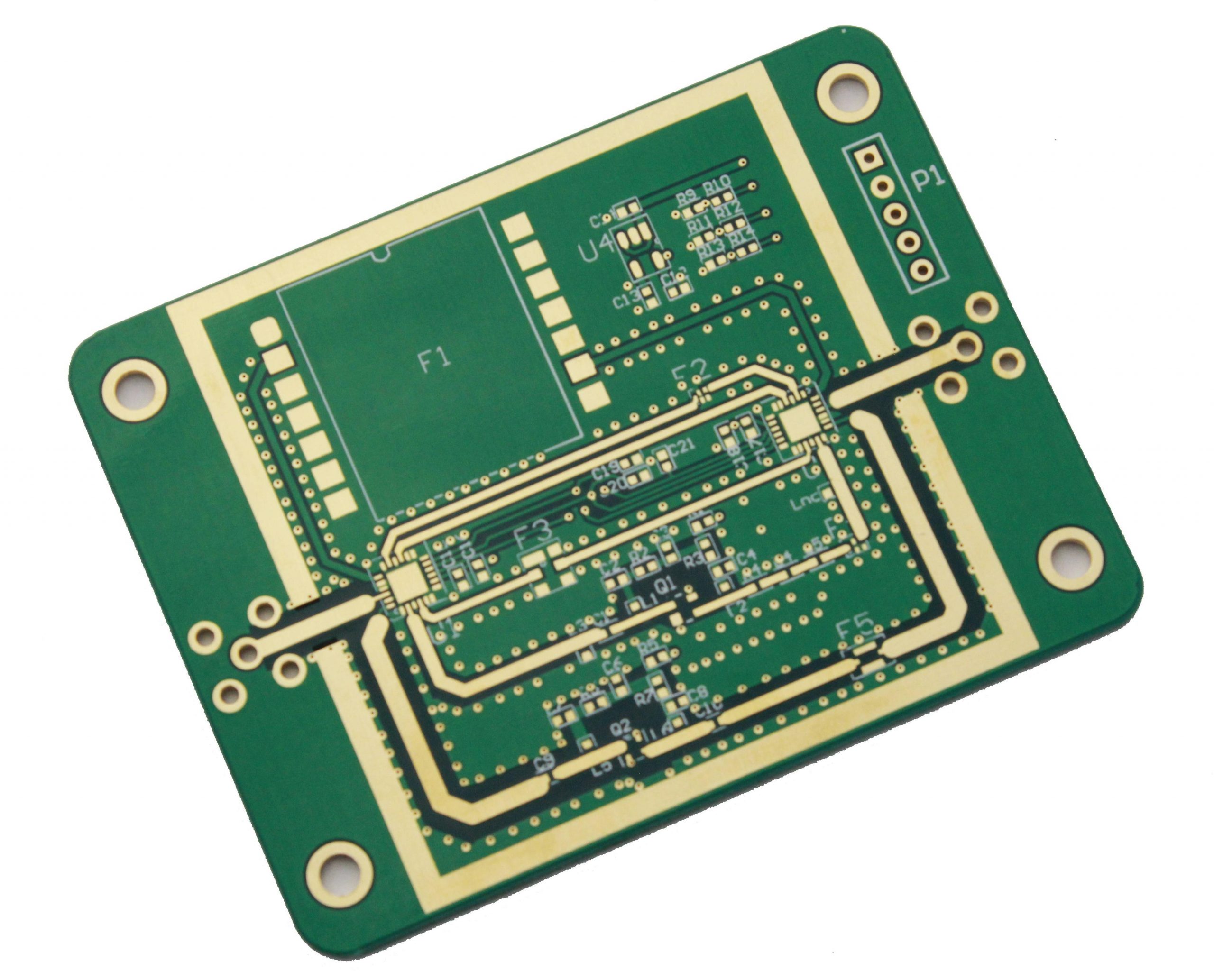
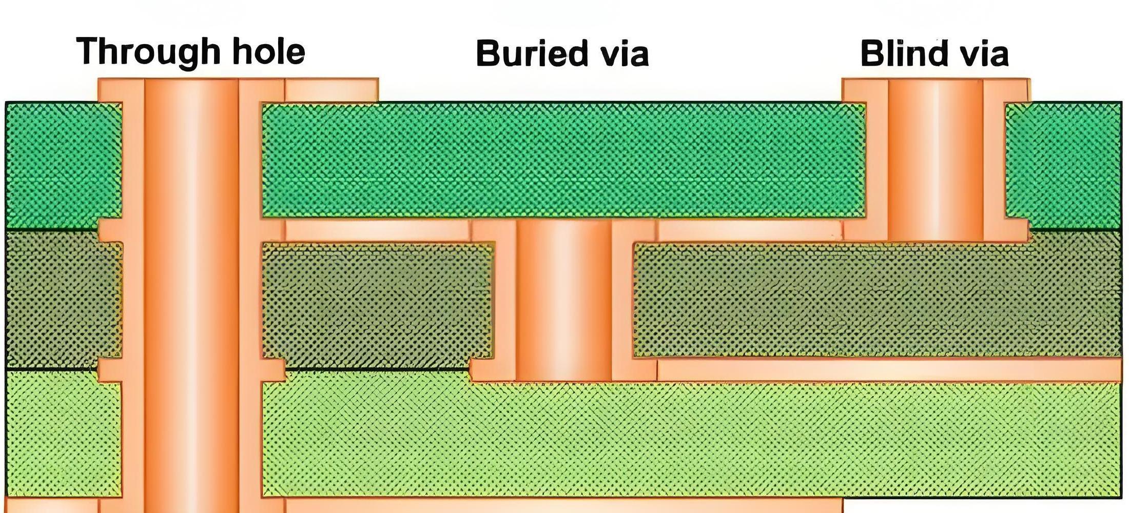
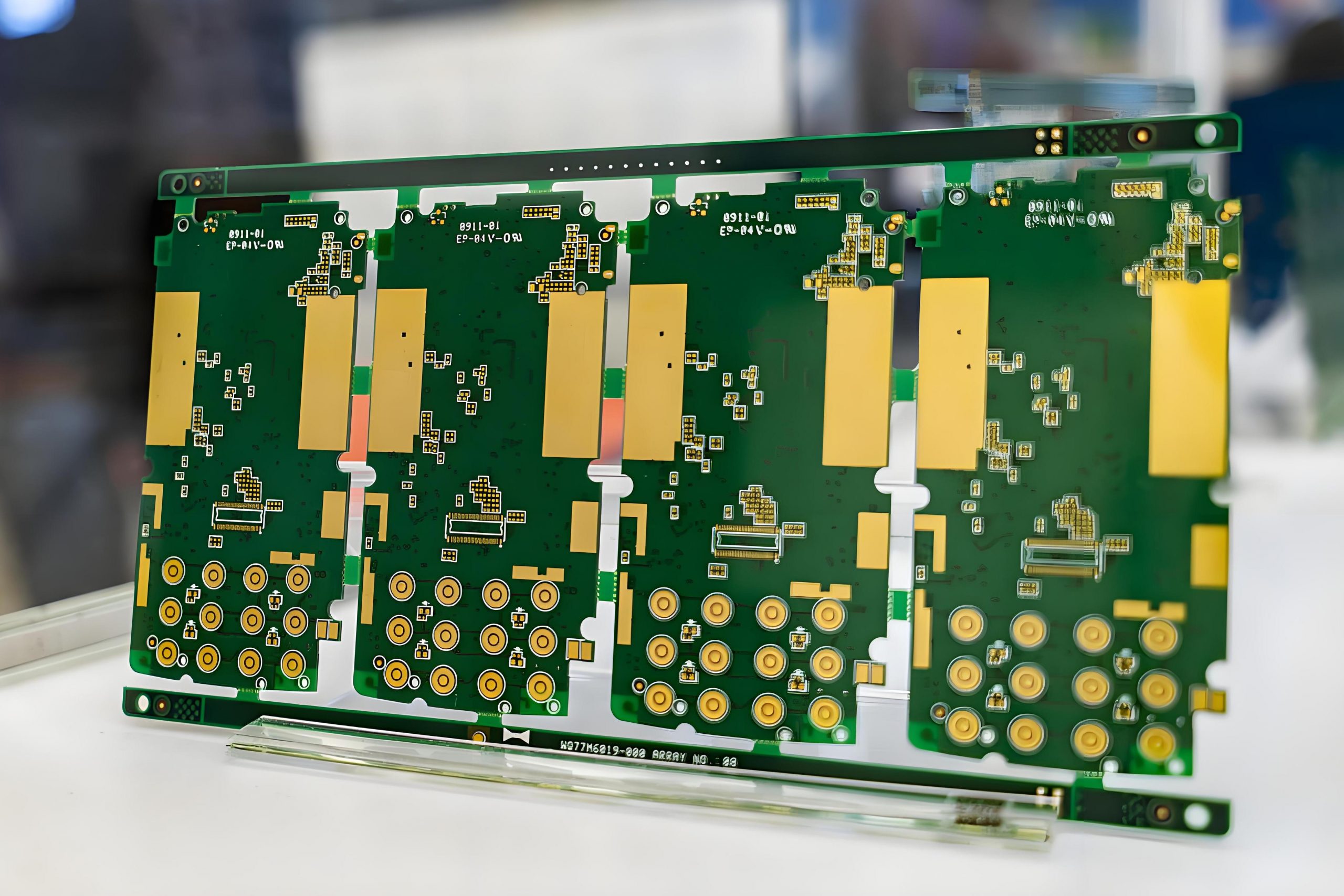
PCB coating is a layer of special material applied on the surface of PCB to protect the circuit board from environmental factors (such as moisture, dust, chemical corrosion, etc.) while improving its electrical insulation, welding performance and mechanical strength. Common coating types include organic coating, metal plating, conformal coating, etc., which are applied by spraying, dipping or brushing.
What is conformal coating on pcb?
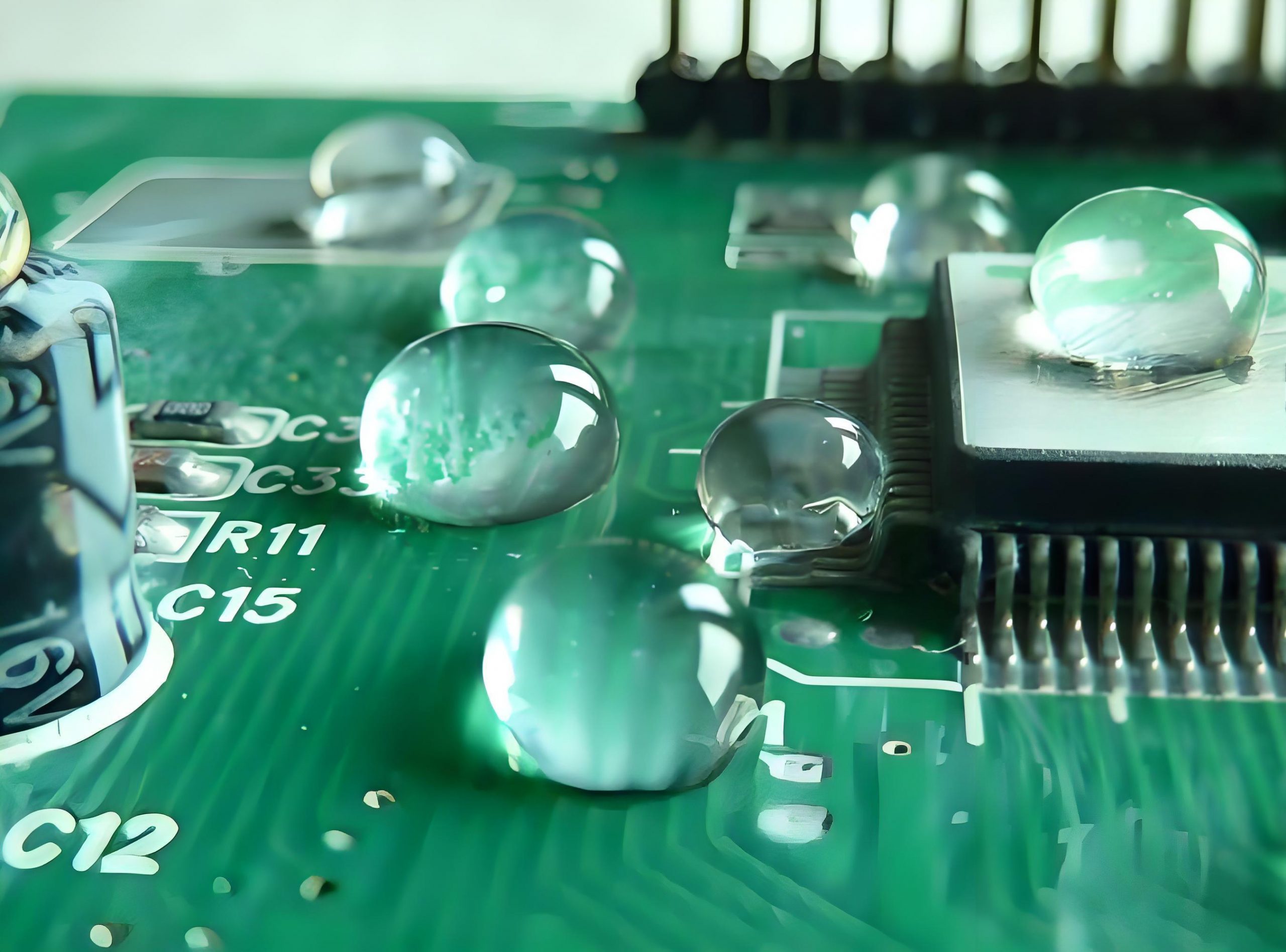
Conformal coating is a protective layer applied to a PCB to shield the board’s components from external contaminants like dust, moisture, and chemicals.
Unlike encapsulation, which surrounds the entire assembly, conformal coating is a thin, flexible layer that conforms to the shape of the PCB and its components. The coating allows the PCB to remain functional while also protecting it from environmental stresses.
The purpose of conformal coating is to enhance the reliability and longevity of PCBs by protecting them from elements that could cause short circuits, corrosion, or other types of damage.
It is particularly critical in industries where the PCB is exposed to harsh environments or where the failure of a PCB could have severe consequences.
Why conformal coating is used in pcb?
There are several reasons why conformal coating is essential for PCBs:
- Protection from Moisture: Moisture is one of the biggest threats to PCBs. The coating provides a moisture-resistant barrier, reducing the risk of corrosion and electrical shorts.
- Dust and Contaminant Shielding: Dust, dirt, and other environmental contaminants can easily find their way onto uncoated PCBs. A conformal coating prevents this by creating a physical barrier.
- Chemical Resistance: Many industrial environments expose PCBs to chemicals, oils, and solvents. A good conformal coating can offer protection against these substances, preserving the integrity of the PCB.
- Electrical Insulation: In certain cases, conformal coatings help isolate electrical components from one another, preventing unwanted connections or short circuits.
- Thermal Resistance: In some instances, conformal coatings can help dissipate heat, allowing the PCB to operate more efficiently in high-temperature environments.
In summary, PCB coatings ensure better reliability, enhanced performance, and longer lifespan, especially in medical, automotive, and aerospace sectors.
Can conformal coating be removed?
Yes, conformal coating can be removed, though the process is often delicate and requires careful handling.
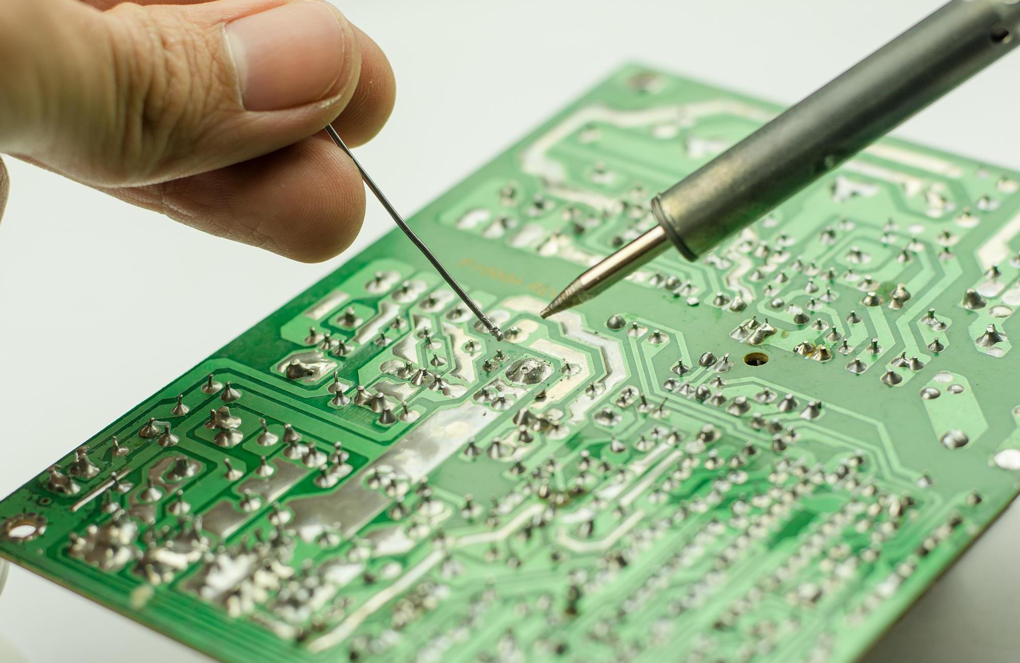
PCB coating removal is generally done when there’s a need for repair, modification, or redesign of the PCB. However, the removal process must be approached with caution to prevent damaging the underlying components.
Some coating removal techniques include using:
- Chemical Strippers: These are special solvents designed to break down and dissolve the coating.
- Mechanical Methods: Using tools like abrasive pads or brushes, the coating can be scrubbed off.
- Heat Application: For certain coatings, heat guns or infrared ovens can soften the coating, making it easier to remove.
Each method should be selected based on the type of coating and the sensitivity of the PCB components.
How to remove conformal coating from pcb?
- Choose the Right Method: Select a removal technique based on the type of coating and the nature of the PCB.
- Use Protective Gear: Always wear gloves, goggles, and a mask to avoid exposure to chemicals and solvents.
- Apply Solvent: If using a chemical stripper, apply it carefully to the PCB using a brush or cloth. Allow the solution to sit for a few minutes to break down the coating.
- Scrub Off the Coating: Use a soft brush or sponge to scrub the coating off. Avoid using hard bristles that could damage the PCB.
- Rinse and Dry: Once the coating has been removed, rinse the PCB with water or alcohol to remove any chemical residues. Allow the PCB to dry completely before reapplying a new coating or proceeding with repairs.
What is the best coating for PCB?
The best coating for PCB depends on various factors, including the environment in which the PCB will operate, the level of protection needed, and the specific requirements of the project.
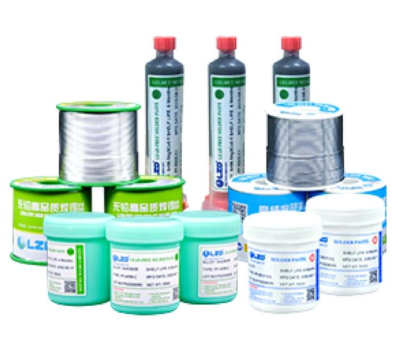
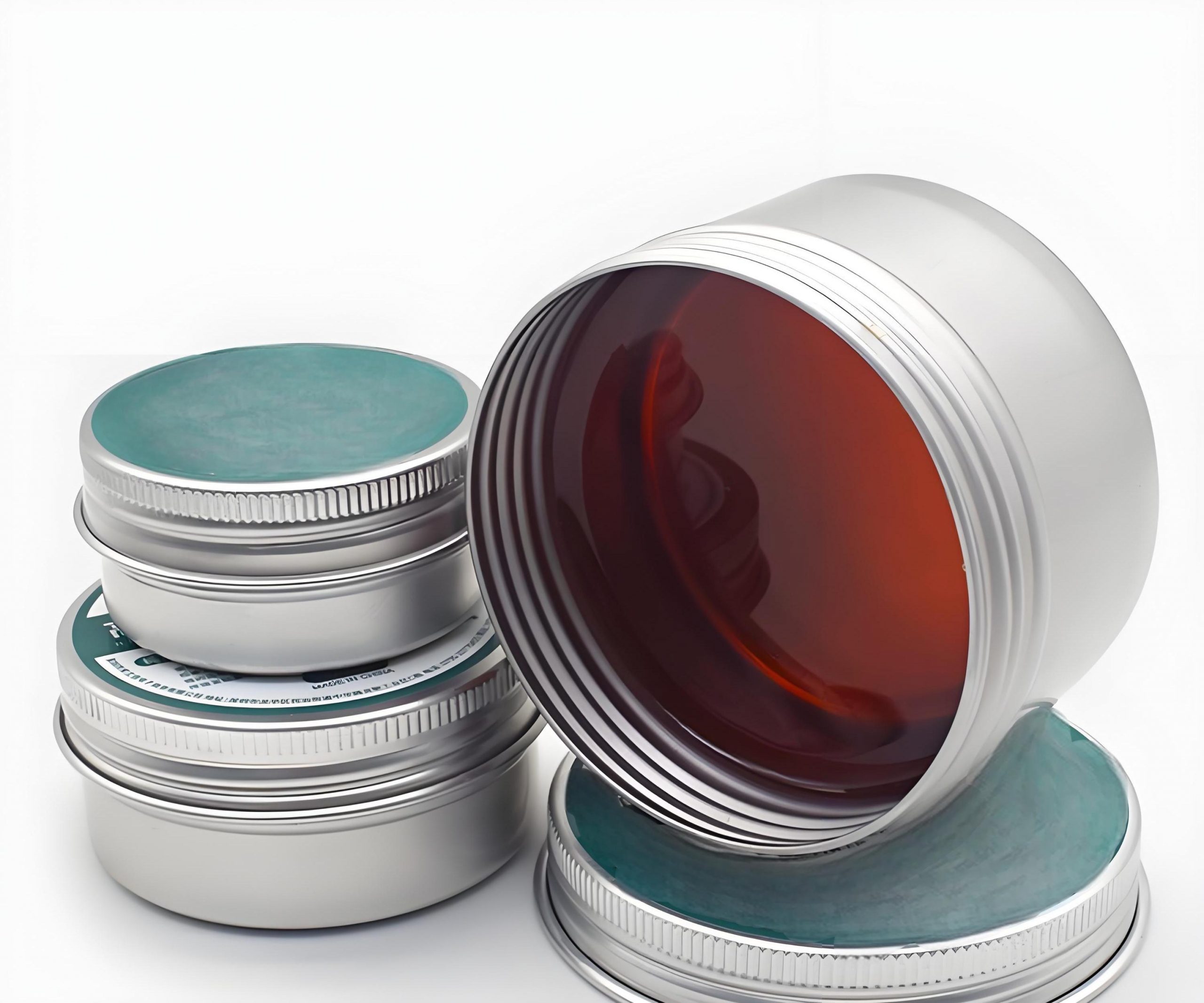
- Acrylic Coating: This is one of the most common PCB coatings due to its excellent moisture resistance, ease of application, and good overall protection. It is clear, which makes it ideal for applications where visual inspection is needed.
- Silicone Coating: Known for its flexibility and high-temperature resistance, silicone coating is often used in PCBs that will be exposed to high heat or thermal cycling.
- Polyurethane Coating: Offering high durability and excellent resistance to environmental factors, polyurethane coating is ideal for industrial applications that require both moisture and chemical resistance.
- Epoxy Coating: Epoxy coatings provide strong protection against mechanical wear and harsh environments but are less flexible than other coatings.
- Parylene Coating: Parylene is a highly effective coating for PCBs, offering protection from chemicals and moisture while maintaining a very thin and uniform layer. It is commonly used in medical and aerospace applications.
Each type has its advantages, so it’s essential to select the one that best fits your needs.
What is the cheapest PCB finish?
When it comes to PCB finishes, the cost can vary widely depending on the type of finish chosen.
Acrylic coatings are often considered among the most affordable options, providing good protection for general applications.
However, when specific environmental conditions require more advanced coatings (like Parylene or silicone), the cost can be higher.
Opting for a lower-quality coating may result in increased wear and tear or reduced protection, leading to failures over time.
How to measure conformal coating thickness?
Too thick a coating can cause unwanted stress on components, while too thin a layer might not provide sufficient protection.
The most common methods for measuring coating thickness are:
- Micrometers: Special digital micrometers can be used to measure the thickness of the coating with great precision.
- Ultrasonic Testing: This non-destructive method uses sound waves to measure the thickness of coatings.
- Coating Thickness Gauges: These handheld tools use electromagnetic induction or eddy current technology to measure coating thickness quickly and accurately.
It’s vital to measure coating thickness regularly during the application process to maintain consistent protection across the entire PCB.
What are the drawbacks of conformal coating?
While conformal coatings offer numerous benefits, there are some drawbacks to consider:
- Limited Protection for Physical Damage: While they protect against moisture and contaminants, coatings don’t provide protection against physical impacts or harsh mechanical stresses.
- Coating Removal Complexity: Removing conformal coatings can be tricky and requires specialized techniques and tools.
- Potential for Uneven Coating: If the coating process is not executed correctly, it could result in areas where the coating is too thick or thin, leading to reduced protection or malfunctioning.
- Increased Component Stresses: Some coatings, especially those that are too thick or rigid, can put additional strain on the components, leading to potential damage over time.
Despite these drawbacks, the benefits of conformal coatings often outweigh the disadvantages, especially when dealing with sensitive electronics exposed to harsh environments.
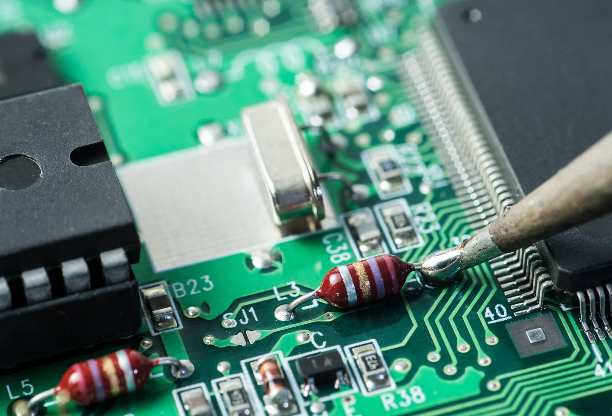
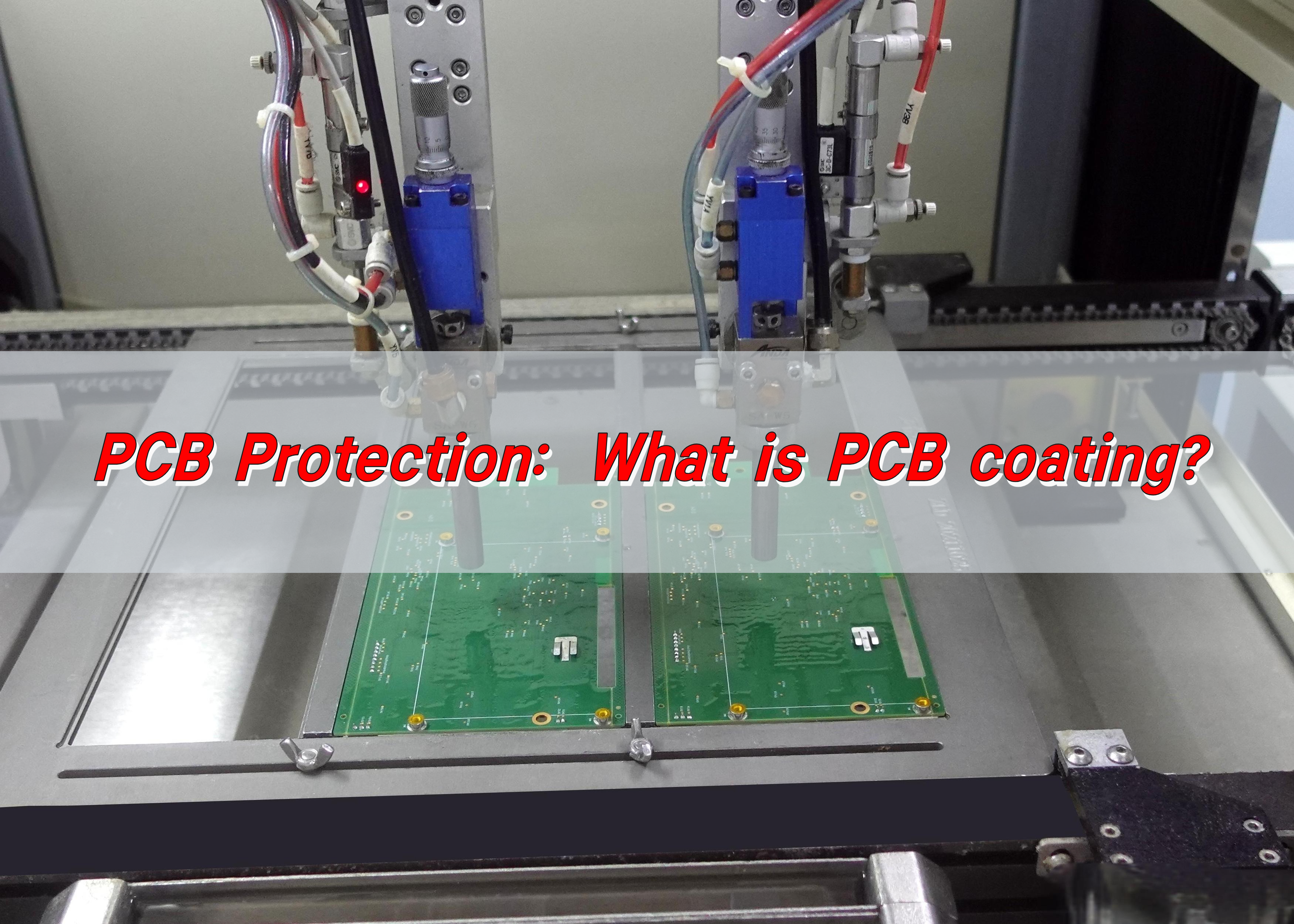
How do you apply conformal coating to PCB?
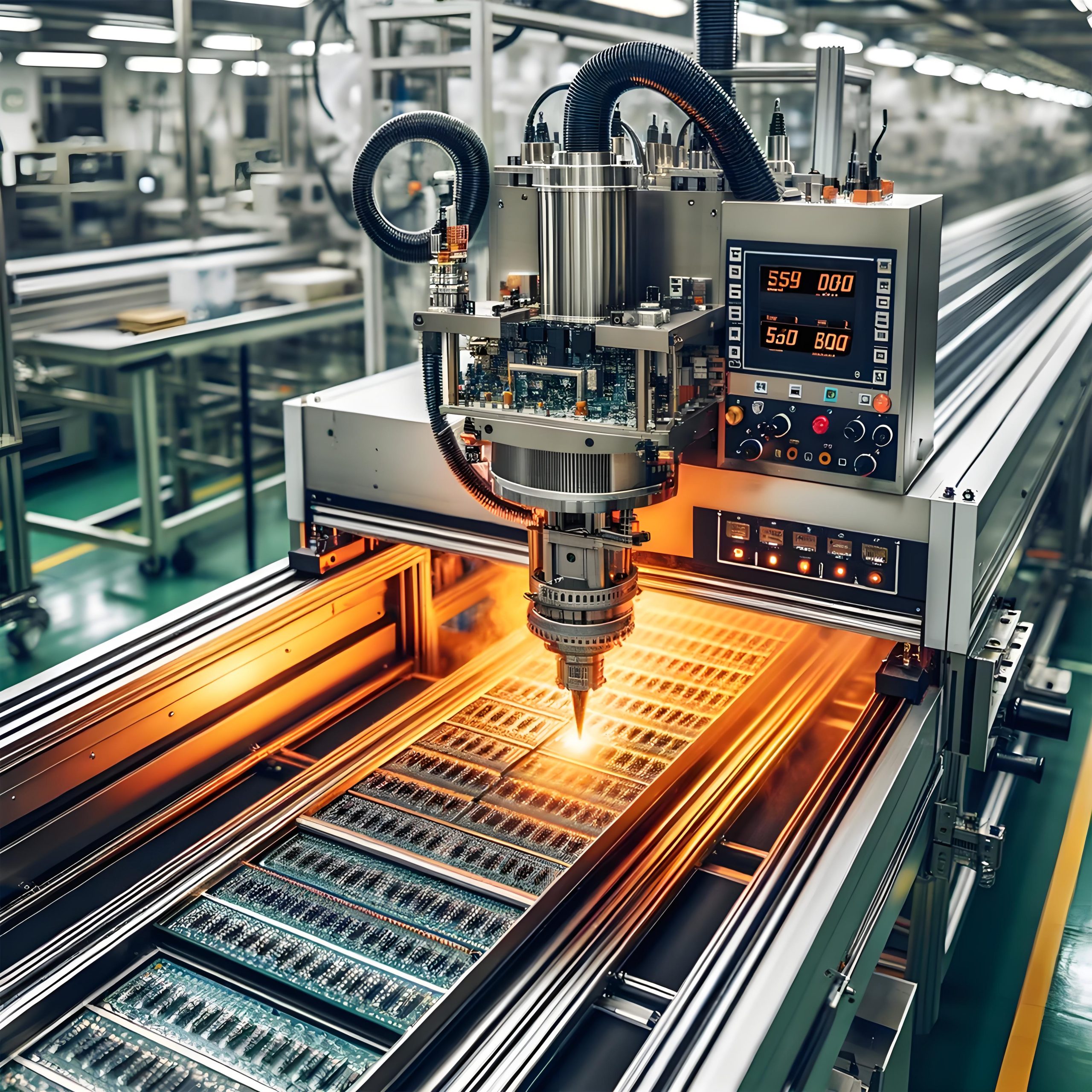
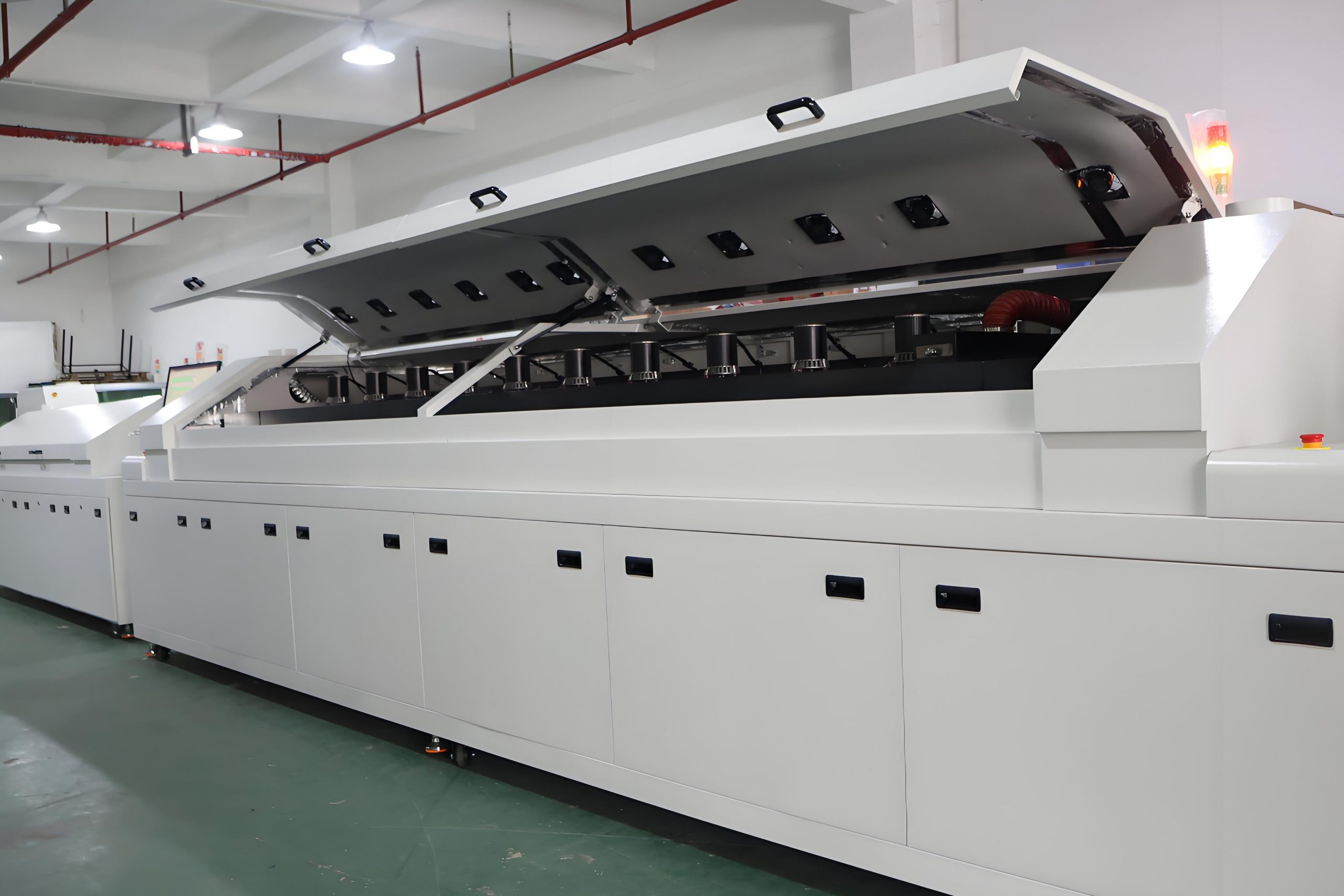
Applying conformal coating to PCBs can be done through several methods, including:
- Spraying: Spray applications are one of the most common methods for applying conformal coatings. It provides even coverage and is suitable for large-scale production.
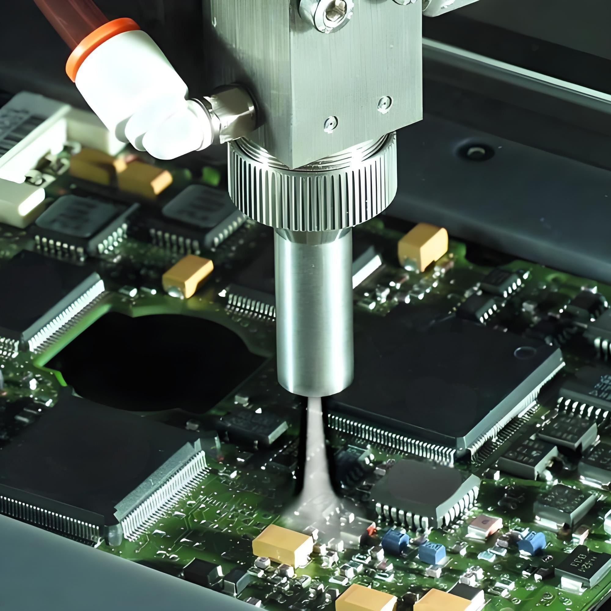
- Dipping: In this method, the entire PCB is dipped into a bath of conformal coating material, allowing it to coat the board evenly.
- Brushing: For smaller batches or repairs, brushing is a viable method.
- Selective Coating Machines: These machines can apply conformal coatings only to the areas of the PCB that need protection, minimizing wastage.
Each method has its benefits, and the choice depends on the specific project and production needs.
Conclusion:
PCB coating is an essential protective measure that ensures PCBs can withstand environmental challenges while maintaining functionality.
At EBest Circuit (Best Technology), Our experienced engineers will help you choose the best solution for your project, ensuring your PCBs are protected and reliable. For more information, contact us at sales@bestpcbs.com