Surface Mount Technology has reshaped how modern electronics are built. From compact consumer devices to high-reliability industrial systems, the SMT line is the backbone that enables consistent, scalable, and precise assembly. If you are evaluating manufacturing partners or planning your own production setup, understanding how an SMT line works is not optional—it is essential.
What is SMT Production Line?
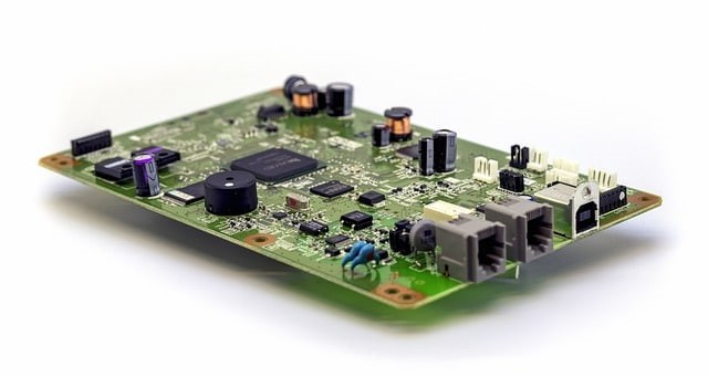
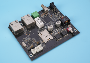
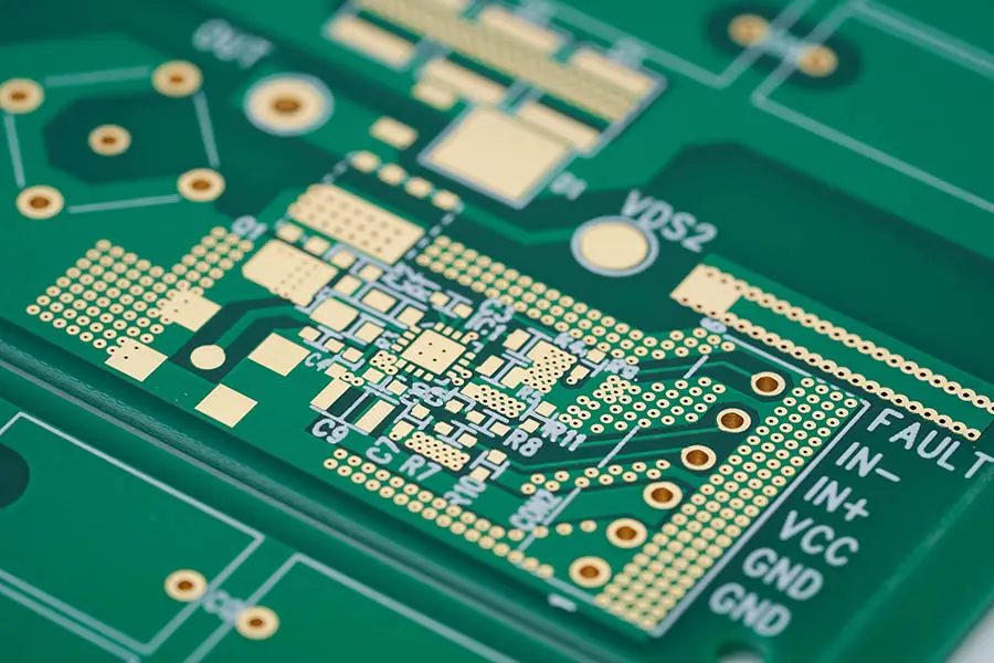
An SMT production line is an integrated sequence of automated machines designed to assemble electronic components directly onto the surface of a printed circuit board. Instead of inserting components through holes, SMT places them on pads and solders them using controlled thermal processes.
At its core, an SMT line is not just a group of machines. It is a synchronized system where material handling, placement accuracy, and thermal profiles are tightly controlled to ensure yield and reliability.
In practical terms, an SMT production line performs three main functions:
- Applies solder paste onto PCB pads
- Places components with high precision
- Reflows solder to create permanent electrical and mechanical connections
This entire process is optimized for speed, repeatability, and traceability.
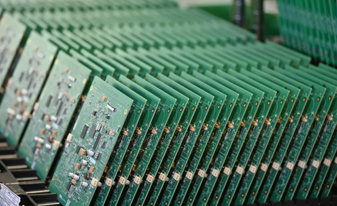
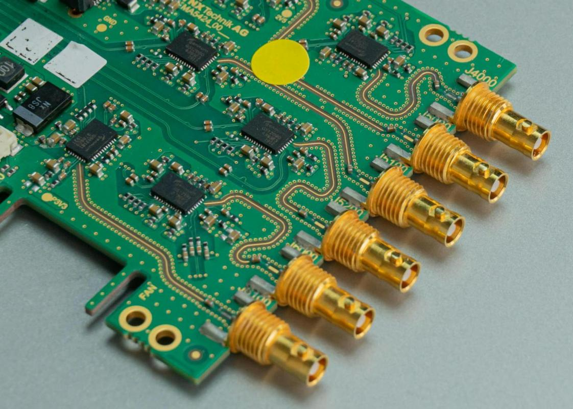
A typical SMT assembly line includes conveyors, printers, pick-and-place machines, ovens, and inspection systems. Each unit communicates with the others to maintain throughput and minimize downtime.
From a manufacturing perspective, SMT lines are preferred because they:
- Support high-density designs such as HDI and fine-pitch BGA
- Enable miniaturization of electronic products
- Reduce manual labor and human error
- Improve production consistency across batches
At EBest Circuit (Best Technology), SMT production lines are configured to support both prototype runs and high-mix, low-volume manufacturing. This flexibility allows engineers to validate designs quickly while maintaining production-level quality.
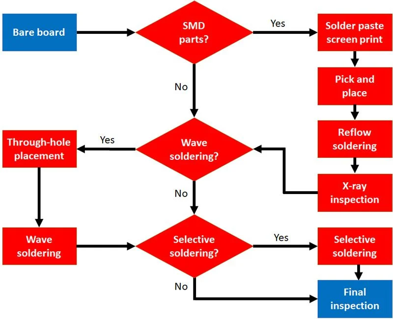
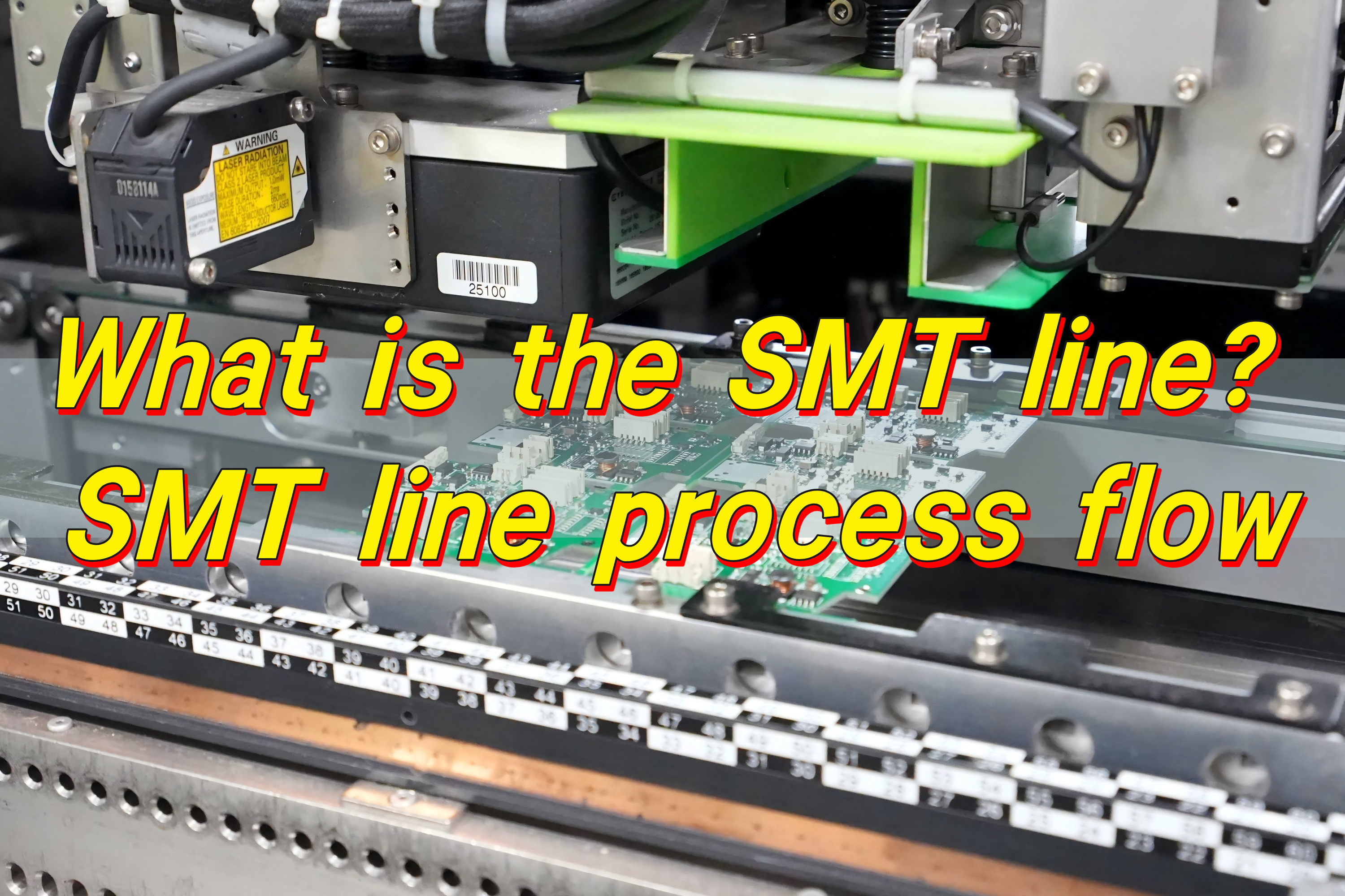
What is SMT Line Process?
The SMT line process is a structured flow that transforms a bare PCB into a fully assembled board. Each step is engineered to maintain alignment, solder integrity, and component accuracy.
Below is a simplified overview of the SMT line process flow:
- PCB loading
- Solder paste printing
- Solder paste inspection (SPI)
- Component placement
- Reflow soldering
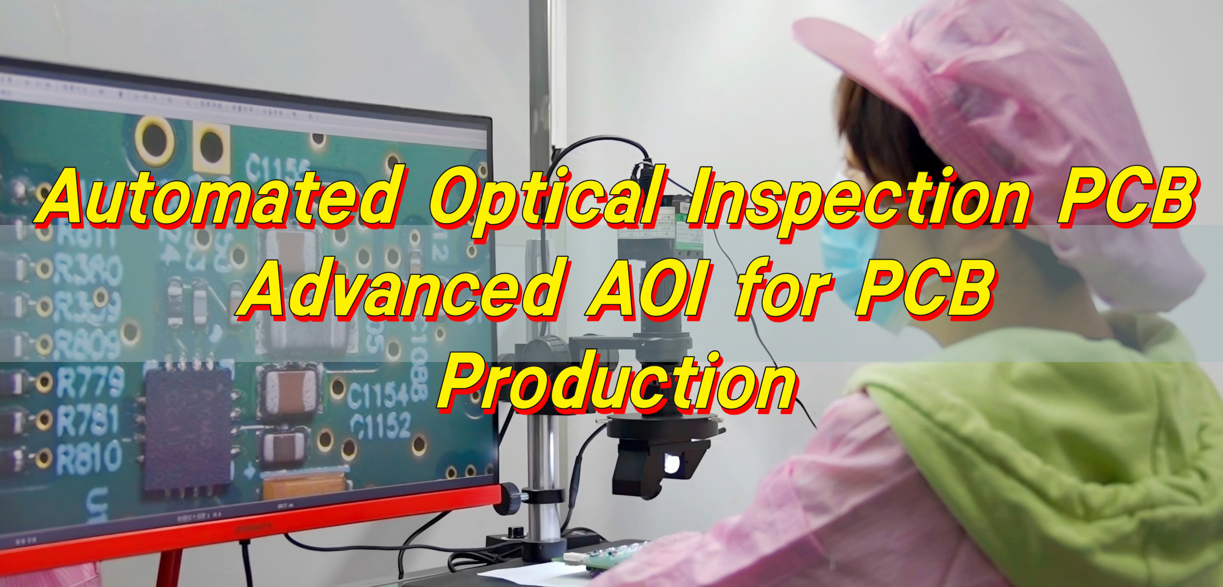
- Automated optical inspection (AOI)
- Optional testing and rework
Each stage plays a specific role in ensuring final product quality.
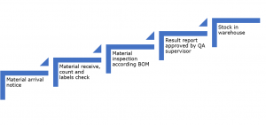
Step-by-Step SMT Line Process Flow
1. PCB Loading
Bare PCBs are loaded onto the conveyor system. Automated loaders ensure consistent positioning and prevent handling damage.
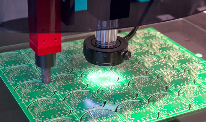
2. Solder Paste Printing
A stencil printer deposits solder paste onto PCB pads. The volume and alignment of paste are critical for proper solder joints.
3. SPI (Solder Paste Inspection)
SPI systems measure paste volume, height, and alignment. Early detection here prevents downstream defects.
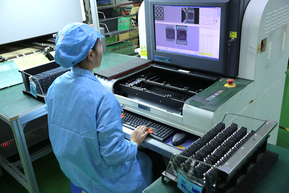
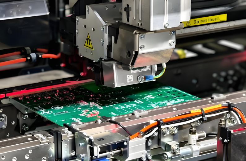
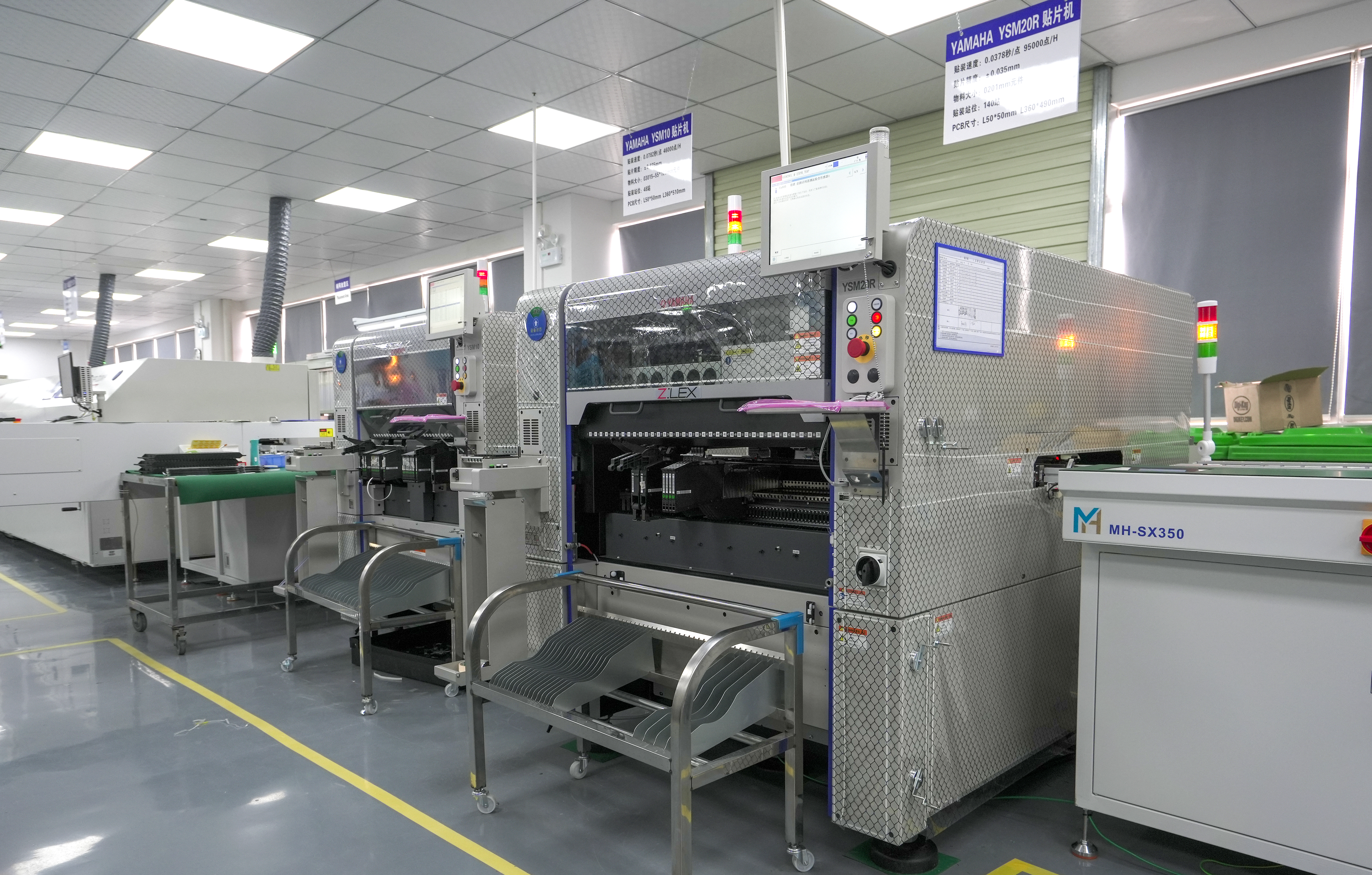
4. Pick-and-Place Process
High-speed placement machines mount components onto the PCB. These machines use vision systems to achieve micrometer-level accuracy.
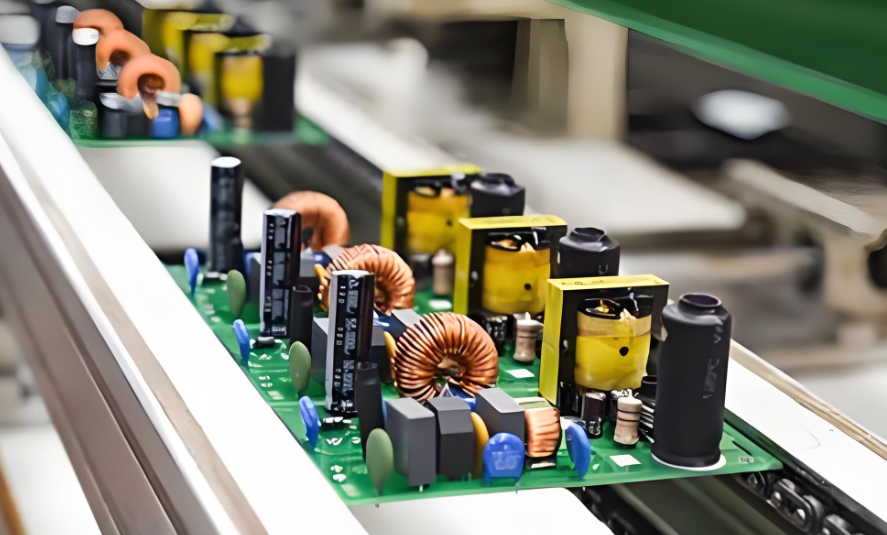
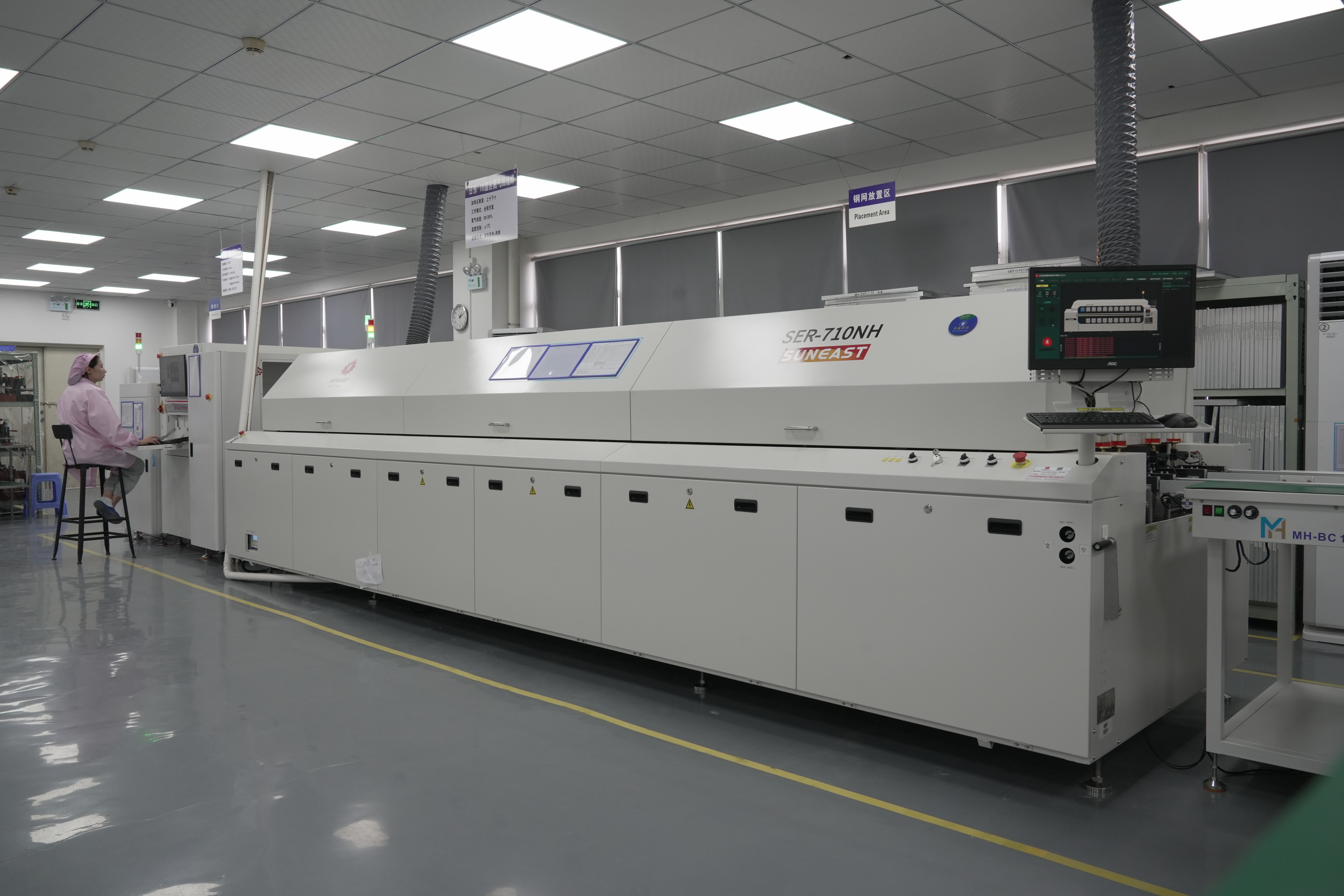
5. Reflow Soldering
Boards pass through a reflow oven where solder paste melts and solidifies, forming reliable joints. Temperature profiles are carefully controlled.
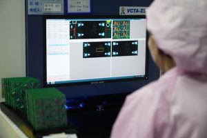
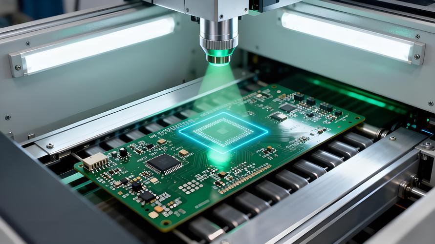
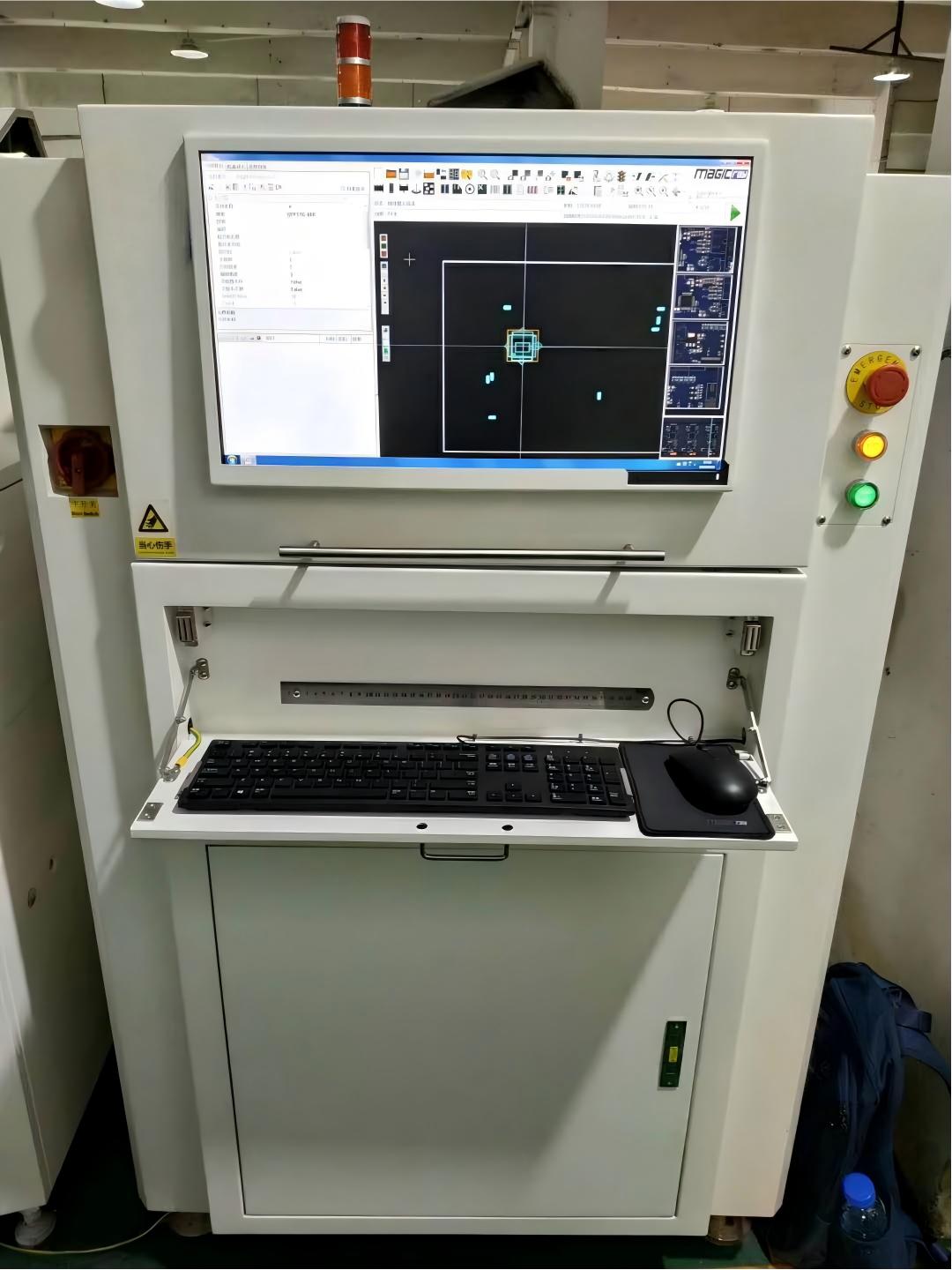
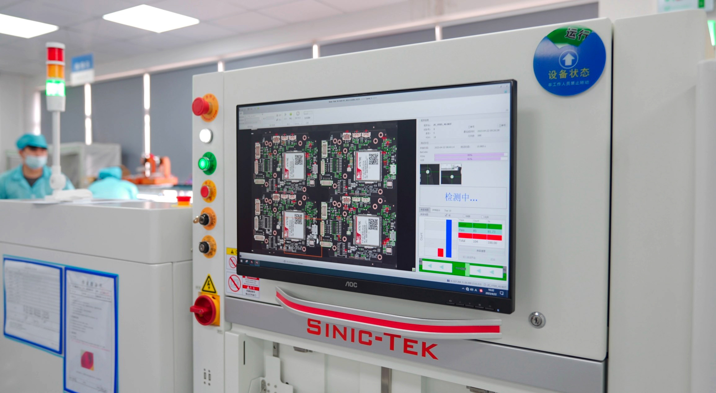
6. AOI (Automated Optical Inspection)
AOI systems inspect component placement, polarity, and solder quality. This step ensures defects are identified before further processing.
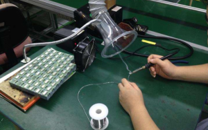
7. Functional Testing (Optional)
Depending on the application, boards may undergo ICT or functional testing to validate electrical performance.
Why Process Control Matters?
Even small variations in solder paste or temperature can affect yield. That is why advanced SMT lines rely on:
- Closed-loop feedback systems
- MES (Manufacturing Execution Systems) for traceability
- Real-time monitoring of process parameters
At EBest Circuit (Best Technology), SMT lines are integrated with MES systems that allow traceability within seconds. This is especially important for industries such as automotive and medical electronics.
What is a SMT Line Operator?
An SMT line operator is responsible for managing, monitoring, and maintaining the production line. While automation handles most of the physical work, human expertise ensures stability and efficiency.
The role is more technical than it may appear. Operators must understand machine behavior, process parameters, and quality standards.
Key Responsibilities
- Setting up machines for new production runs
- Loading components and feeders
- Monitoring machine performance
- Adjusting process parameters when needed
- Identifying and resolving minor issues
- Coordinating with engineers for process optimization
Skill Requirements
A capable SMT operator typically has:
- Basic understanding of electronics and PCB assembly
- Familiarity with SMT equipment interfaces
- Attention to detail and process discipline
- Ability to interpret inspection results
In advanced facilities, operators often work alongside process engineers. This collaboration ensures that production remains stable while continuously improving yield.
Can a Solitary Operator Run SMT Line Efficiently?
In theory, a single operator can run a small SMT line. In practice, efficiency depends on the complexity of the line and production volume.
When One Operator Can Work?
A solitary operator may manage the line effectively if:
- The line is compact and semi-automated
- Production volume is low
- Product complexity is limited
- Machines are well-maintained and stable
Limitations of Single-Operator Setup
However, there are constraints:
- Limited ability to handle multiple issues simultaneously
- Slower response to machine alarms
- Reduced throughput
- Increased risk of production delays
Recommended Approach
For most professional environments, a small team is preferred:
- One operator for printing and placement
- One technician for inspection and troubleshooting
- One engineer for process oversight
This structure ensures balance between efficiency and quality.
At EBest Circuit (Best Technology), SMT lines are staffed based on project complexity. This ensures consistent output without compromising quality or delivery timelines.
How Do You Add Serialization to an SMT Line?
Serialization is essential for traceability. It allows each PCB to be uniquely identified and tracked throughout its lifecycle.
Why Serialization Matters?
- Enables product traceability for compliance
- Supports quality analysis and failure tracking
- Helps with warranty and recall management
- Provides full production history
Methods to Add Serialization
Serialization can be integrated into an SMT line using several methods:
- Laser marking systems
- Inkjet printing
- Barcode or QR code labeling
Integration Steps
- Assign a unique ID to each PCB
- Print or mark the ID before or after SMT process
- Capture data at each stage (SPI, AOI, testing)
- Store data in MES system
Practical Implementation
In a modern SMT line, scanners are installed at key points. Each board is scanned, and data is logged automatically.
At EBest Circuit (Best Technology), serialization is integrated into the MES system. This allows customers to trace materials, processes, and inspection results within seconds.
How to Setup a Small SMT Production Line?
Setting up a small SMT line requires balancing cost, capability, and scalability. The goal is to create a system that meets current needs while allowing future expansion.
Key Considerations
- Production volume
- Product complexity
- Available space
- Budget constraints
Basic Setup for Small SMT Line
A minimal configuration includes:
- PCB loader or manual feeding system
- Stencil printer
- Pick-and-place machine
- Reflow oven
- AOI system
Layout Strategy
A linear layout is often preferred for small setups:
- Improves workflow
- Reduces handling time
- Simplifies operator management
Example Setup
| Equipment | Function | Priority |
|---|---|---|
| Stencil Printer | Solder paste application | Essential |
| Pick-and-Place | Component mounting | Essential |
| Reflow Oven | Soldering | Essential |
| AOI | Inspection | Recommended |
| SPI | Paste inspection | Optional but valuable |
Practical Advice
Start with essential equipment and upgrade as production grows. Avoid over-investing in capacity that is not yet required.
EBest Circuit (Best Technology) supports customers in early-stage production by offering quick-turn SMT assembly services. This allows design validation before committing to full-scale production.
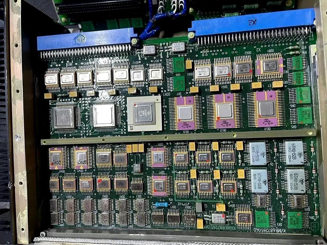
What Equipment is Included in an SMT Line?
An SMT line consists of multiple specialized machines. Each one contributes to a specific stage of the process.
Core Equipment List
- PCB Loader/Unloader
- Stencil Printer
- SPI Machine
- Pick-and-Place Machine
- Reflow Oven
- AOI System
- Conveyor System
Detailed Equipment Breakdown
| Equipment | Function | Key Feature |
|---|---|---|
| PCB Loader | Feeds boards into line | Automation |
| Stencil Printer | Applies solder paste | High precision alignment |
| SPI | Inspects paste quality | 3D measurement |
| Pick-and-Place | Mounts components | High speed & accuracy |
| Reflow Oven | Solders components | Controlled thermal profile |
| AOI | Inspects assembly | Defect detection |
| Conveyor | Transfers boards | Smooth flow |
Advanced Equipment
For high-reliability applications, additional systems may be included:
- X-ray inspection for BGA
- ICT (In-Circuit Testing)
- Functional testing stations
At EBest Circuit (Best Technology), SMT lines are equipped with advanced inspection tools such as AOI and X-ray systems to meet stringent quality standards.
How Much Does an SMT Line Cost?
The cost of an SMT line varies widely depending on scale, automation level, and equipment brand.
Cost Breakdown
| Setup Type | Estimated Cost Range |
|---|---|
| Entry-Level Line | $50,000 – $150,000 |
| Mid-Range Line | $200,000 – $500,000 |
| High-End Fully Automated Line | $800,000 – $2,000,000+ |
Key Cost Drivers
- Pick-and-place machine capability
- Inspection systems (AOI, X-ray)
- Automation level
- Production speed requirements
- Brand selection (e.g., Panasonic, Yamaha, Fuji)
Brand Comparison (Simplified)
| Brand | Strength | Typical Use |
|---|---|---|
| Panasonic | High precision | Automotive, medical |
| Yamaha | Cost-effective | General electronics |
| Fuji | High speed | Mass production |
Strategic Insight
Instead of investing heavily upfront, many companies outsource SMT assembly during early stages. This approach reduces risk and allows faster market entry.
EBest Circuit (Best Technology) offers flexible SMT services with no minimum order requirement. This makes it easier for engineers and startups to move from prototype to production without large capital investment.
Summary:
The SMT line is the core of modern electronics manufacturing. It combines precision machinery, controlled processes, and data-driven systems to deliver reliable PCB assemblies at scale.
If you are exploring SMT production or looking for a reliable manufacturing partner, feel free to reach out: Contact: sales@bestpcbs.com