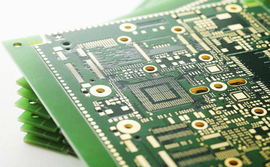
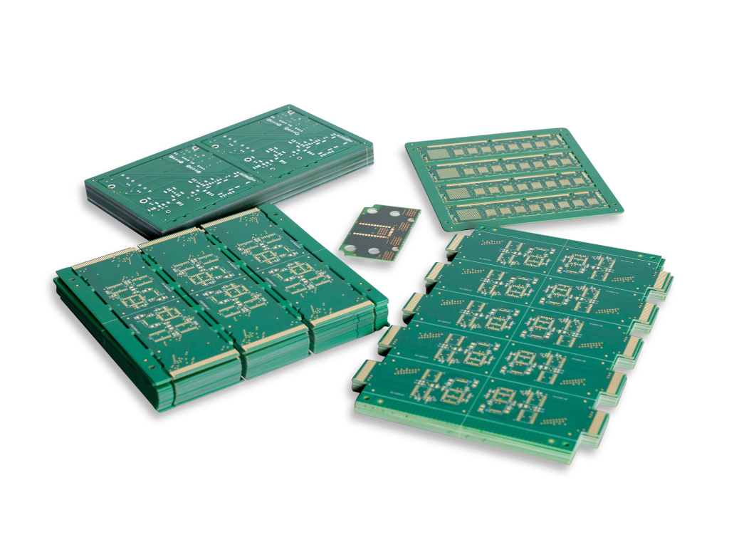
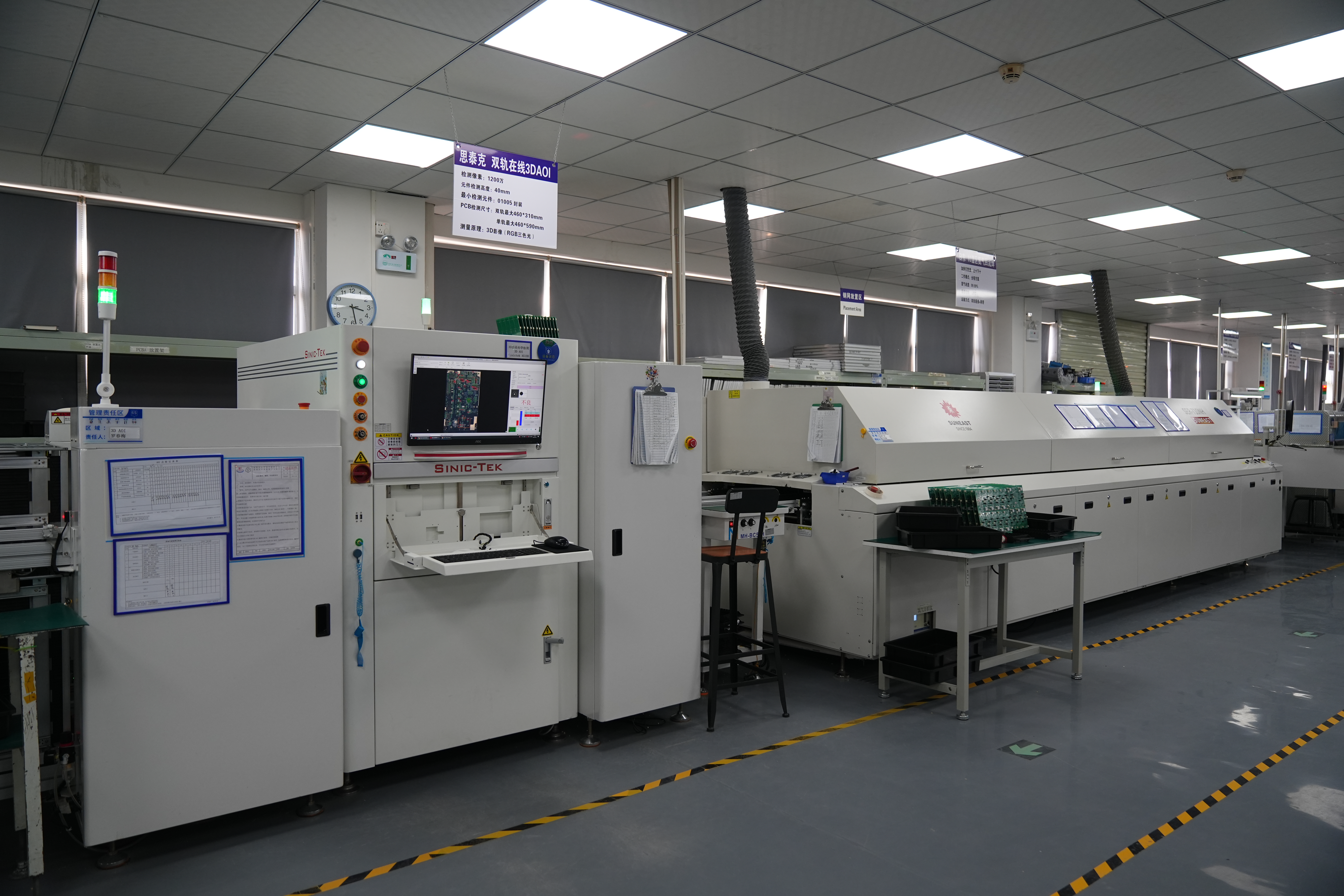
The reflow soldering process is one of the most important steps in modern electronics manufacturing. It links every part of a PCB assembly line, from solder paste printing to final inspection. It also plays a direct role in reliability, long-term stability, and overall product success.
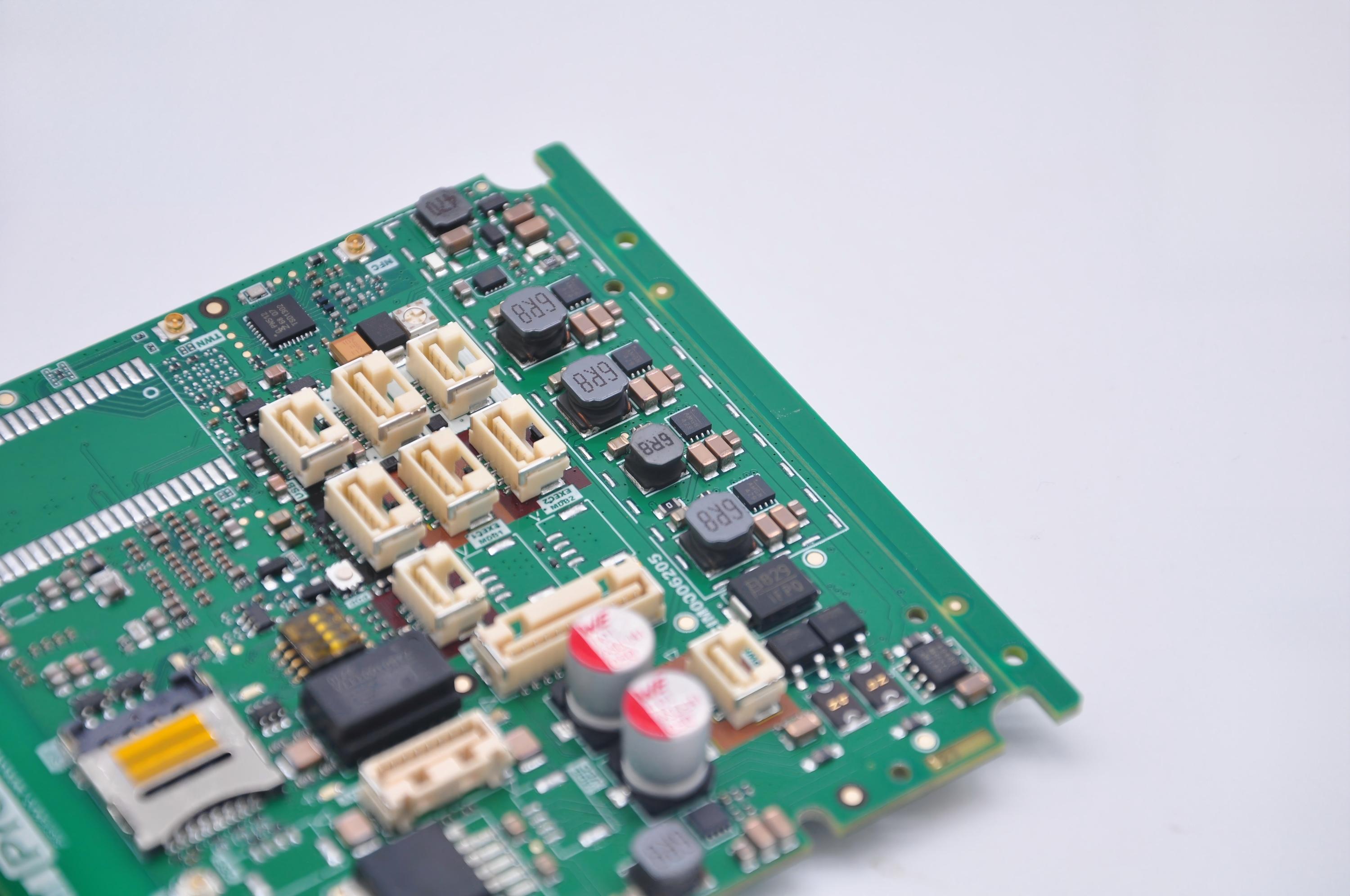
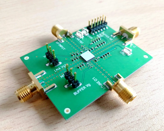
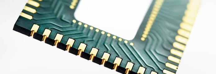
Today, reflow soldering is used for almost every surface mount component. It supports high-density PCBs, fine-pitch packages, micro-BGAs, CSPs, and modern compact devices that require precision.
What Is Reflow Soldering Process in Electronics Manufacturing?
The reflow soldering process is a thermal method used to attach electronic components to pads on a printed circuit board. During the process, solder paste is first applied to copper pads. Components are then placed on top of the paste. After that, the PCB assembly enters a reflow oven where the solder paste melts and forms permanent joints.
The key idea behind reflow process soldering is controlled heat. Every stage of the temperature profile is designed to move slowly and safely through heating zones. Each zone prepares the solder paste and components for the next transition.
Reflow soldering is especially popular because it supports high throughput. It is suitable for large-scale production lines and automated SMT assembly. It delivers reliable results with stable mechanical strength. It also allows manufacturers to assemble complex multi-layer boards with hundreds or thousands of components.
Another advantage is flexibility. The SMT reflow process works with leaded and lead-free solder paste. It also supports various PCB materials, including FR-4, aluminum substrates, flexible circuits, and hybrid boards. With optimized temperature control, it ensures excellent results even on sensitive components such as sensors, small chips, and delicate IC packages.
Which Steps Define the Reflow Soldering Process Step by Step?
The reflow soldering process step by step includes six main phases. Each phase contributes to the final solder joint formation. These steps must run in the correct order, with consistent timing and temperature control.
- Step 1: Solder Paste Application
Every reflow soldering process begins with accurate paste printing. A stencil aligns with PCB pads, and solder paste is applied through stencil openings. The paste must be uniform.
- Step 2: Component Placement
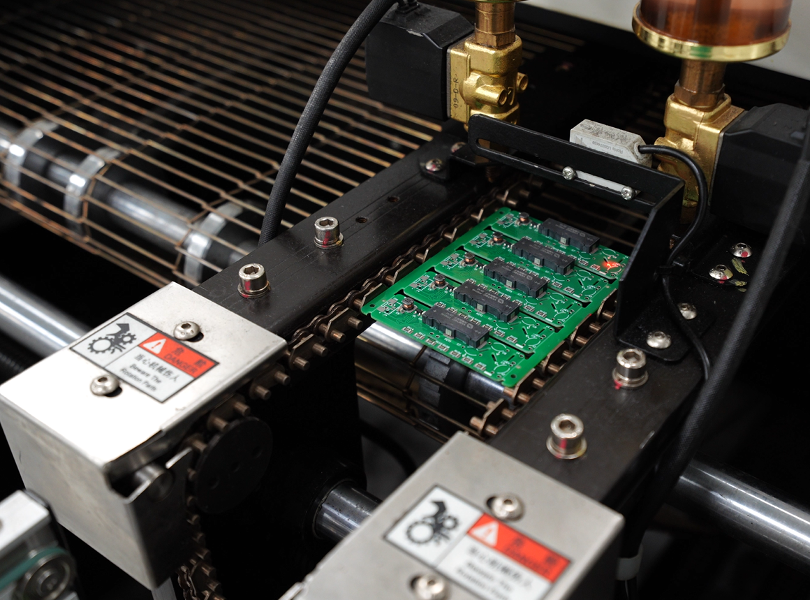
After paste printing, SMT components are placed using pick-and-place machines. These machines locate pads and place each part with high accuracy. The solder paste holds components temporarily due to its tackiness.
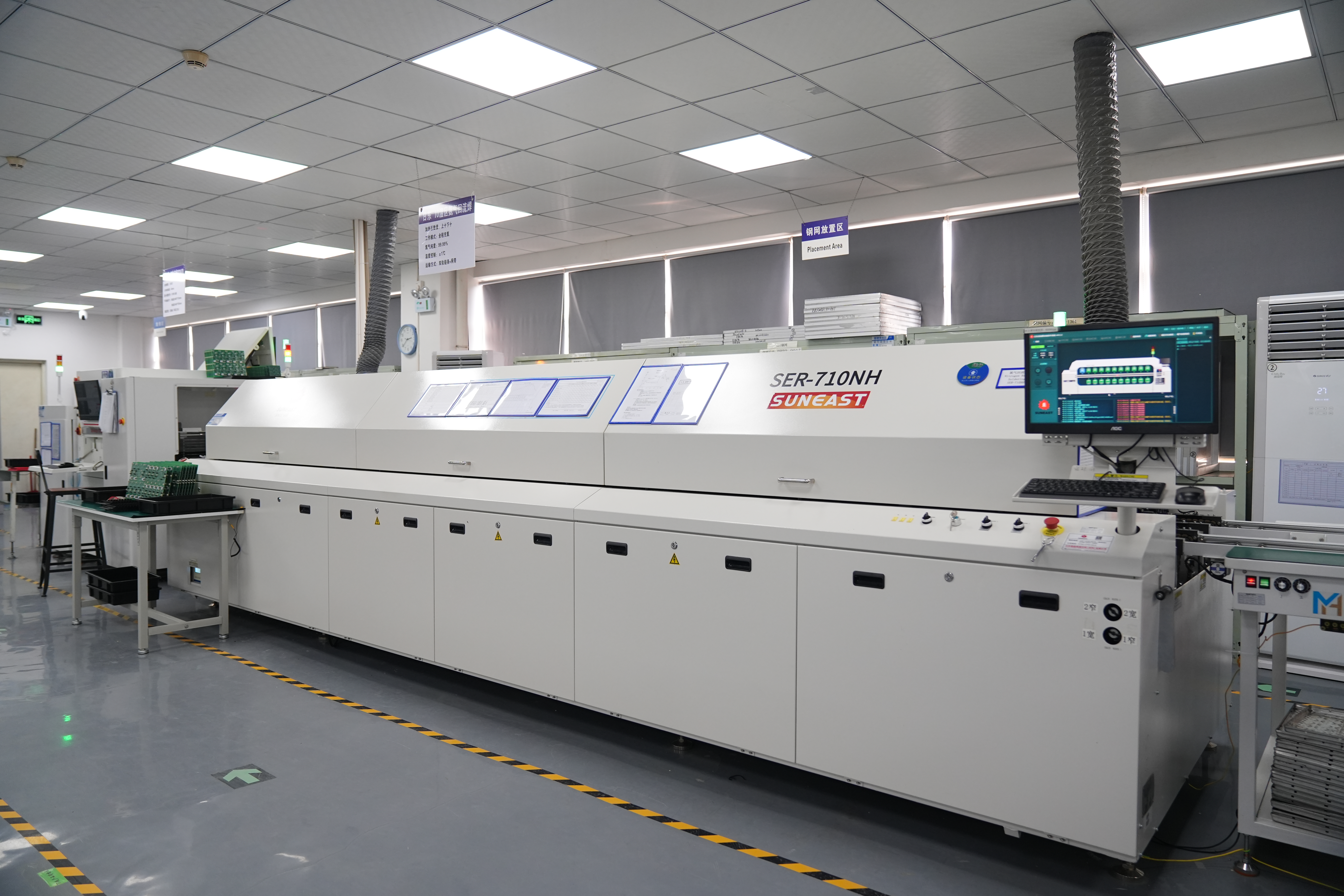
- Step 3: Entry into the Reflow Oven
The PCB assembly enters the reflow oven on a conveyor. The oven includes multiple heating zones. Each zone has its own temperature and airflow control.
- Step 4: Preheat and Soak Stages
As the assembly moves through the preheat zone, the board warms slowly. This step activates flux in the solder paste. It also prepares components for stronger wetting later. The soak zone equalizes PCB temperatures and ensures every part reaches similar thermal levels.
- Step 5: Reflow Zone
Next, the PCB enters the zone where solder paste reaches peak reflow soldering temperature. At this moment, the solder melts and forms solid connections.
- Step 6: Cooling Stage
Once melting occurs, the assembly moves into cooling zones. Proper cooling forms smooth, solid joints. A stable cooling rate prevents defects. When the solder hardens fully, the PCB becomes ready for inspection and testing.
Each stage in the SMT reflow process must be optimized. Even small changes can affect joint quality, component stability, or long-term reliability. When done correctly, however, the full process creates strong, durable, and dependable solder connections.
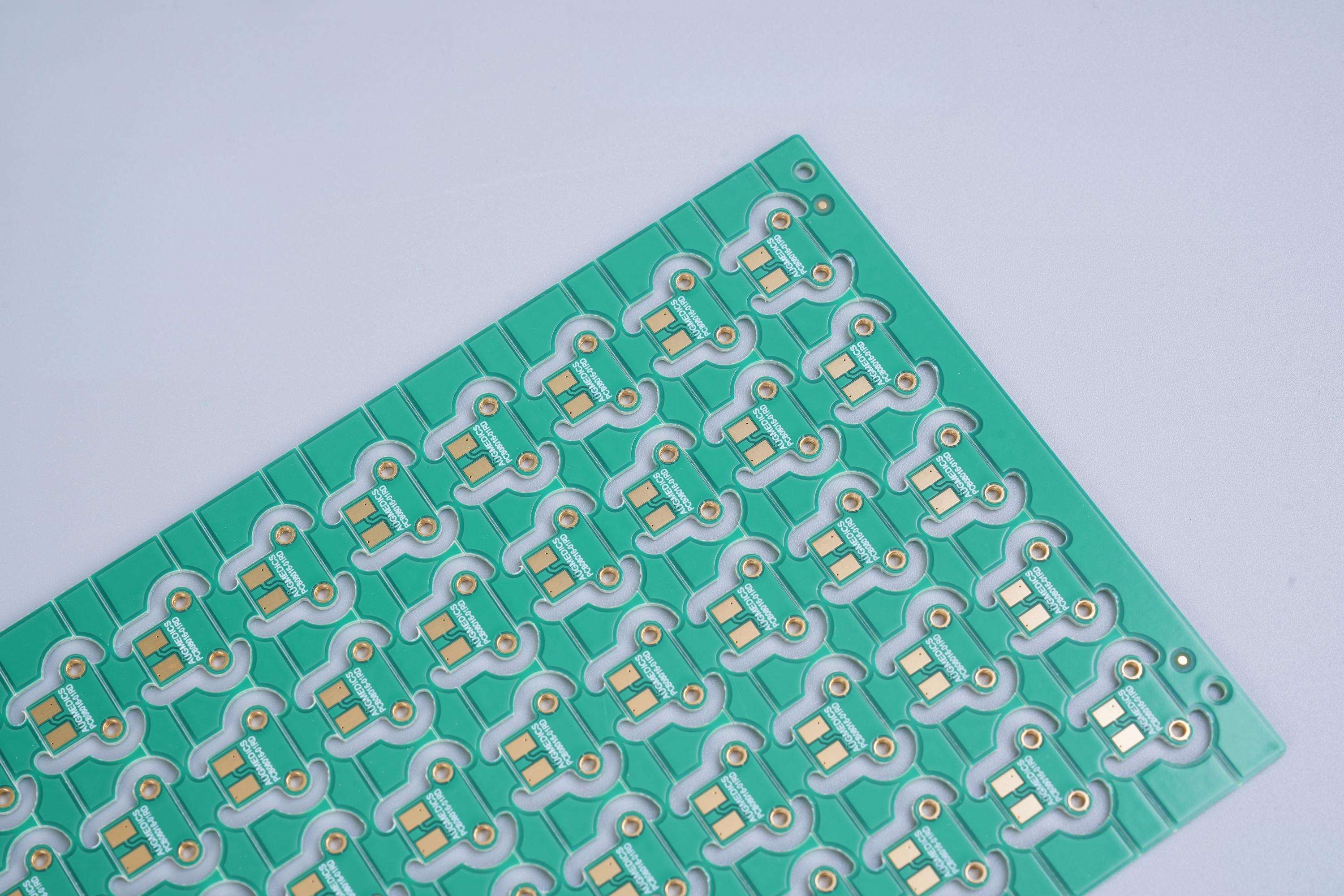
What Is the Composition of Solder Paste Used for Reflow Soldering Process?
Solder paste is a mixture of metal solder powder and flux. Both portions serve critical functions. Together, they enable clean wetting and strong mechanical bonding during the reflow soldering process.
The metal portion typically contains tin, silver, and copper for lead-free versions. Common formulas include SAC305 and SAC405. Leaded solder paste often uses Sn63/Pb37 for stable melting behavior. The spherical metal particles inside the paste make up about 85% to 90% of its total weight.
Flux is the second component. It removes oxides during heating. It also helps metal wet the pads smoothly. Flux mixtures include activators, resins, solvents, and additives. These improve paste stability and support proper printability.
BEST Technology select solder paste formulas based on application needs. Factors include melting point, wetting behavior, stencil thickness, PCB material, pad design, and component type. Proper paste guarantees cleaner joints and better strength.
Good solder paste also improves production efficiency. It prints smoothly, releases cleanly from stencils, and holds components in place. During heating, a high-quality formula creates bright and reliable solder joints with minimal voiding.
Without the right solder paste, the reflow process soldering workflow becomes harder to control. Therefore, paste selection is always a key step in surface mount production.
Which Is the Second Stage in the Reflow Soldering Process?
The second stage in the reflow soldering process is the component placement stage.
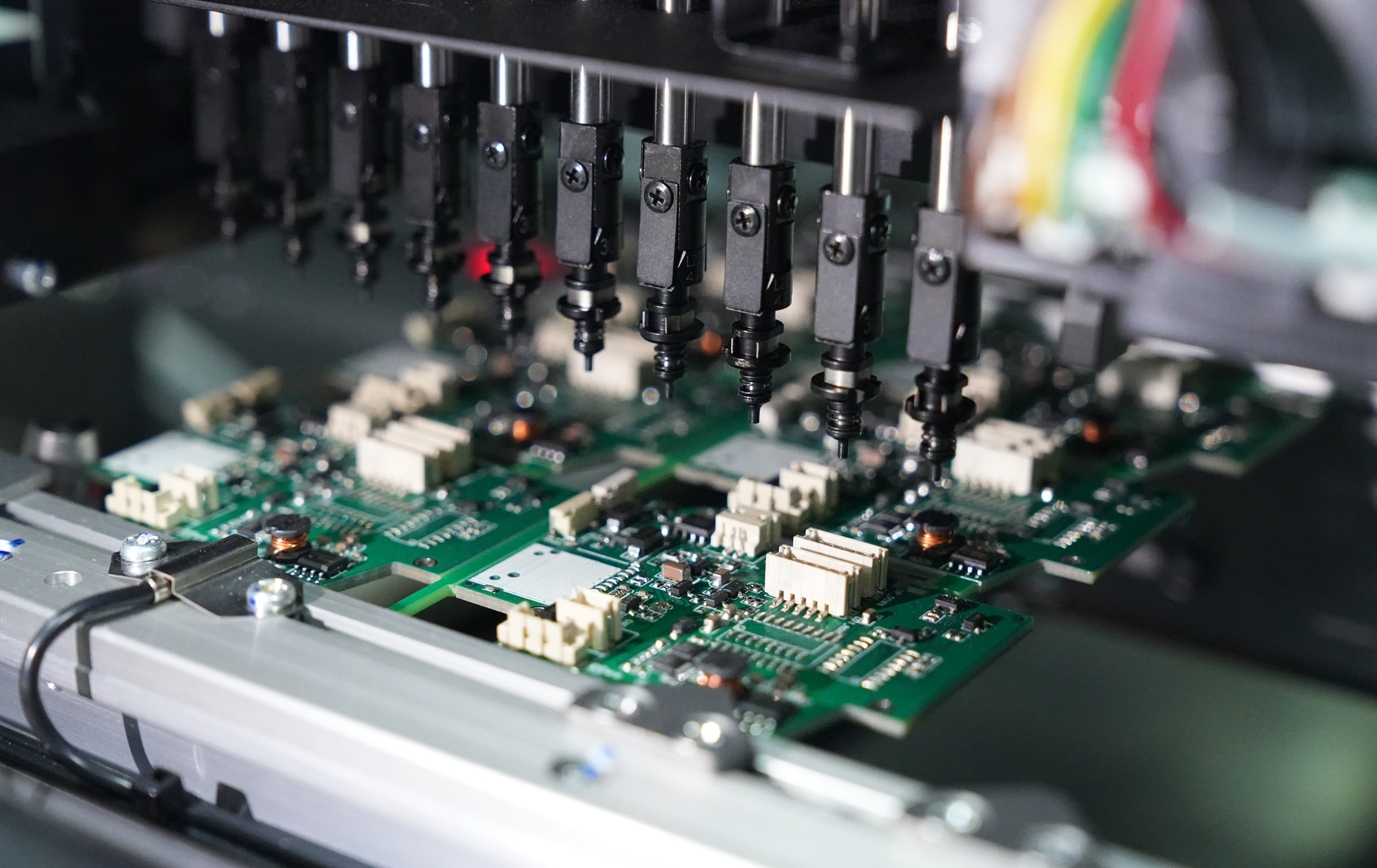
After solder paste application, the next job is placing components onto the PCB. Automated machines handle most of this work. These machines operate at high speed with precise accuracy. They inspect orientation and place each part exactly on its corresponding pad.
Component placement determines how well joints will form in later stages. Proper alignment lowers the risk of tombstoning, bridging, and misalignment defects.
During this stage, the tackiness of solder paste temporarily secures each component. This temporary hold is critical. It allows the PCB to travel safely through the reflow oven without parts shifting.
Which Zone Is the Lengthiest in the Reflow Soldering Process?
The lengthiest zone in the reflow soldering process is the soak zone.
This zone is designed to equalize temperatures across the entire PCB. It helps large components and small components reach similar heat levels. If the PCB does not heat uniformly, defects can occur later. Uneven heating can also impact solder wetting.
In the soak zone, the temperature rises slowly and stays stable for a controlled time. This period activates flux and prepares the solder paste for full melting. The soak zone is typically longer than the preheat or reflow zones because the board needs enough time to stabilize.
Its goal is simple: maintain consistent thermal balance. This balance reduces stress, lowers voiding risk, and improves overall solder quality.
What Is the Cooling Rate Suggested for Reflow Soldering Process?
The recommended cooling rate for the reflow soldering process ranges from 3°C to 4°C per second.
A controlled cooling rate is essential. Cooling too fast can lead to solder cracking. Cooling too slow can create dull joints or grainy structures. The goal is to solidify the molten solder smoothly with a uniform crystalline structure.
Proper cooling also enhances mechanical strength. When the solder cools at the right pace, joints become dense and stable. This stability supports long-term reliability even in high-stress environments such as automotive or industrial electronics.
Modern reflow ovens manage cooling using forced air or nitrogen. Both methods ensure fast and even temperature drops.
At Which Zone Is the Maximum Allowable Temperature of the Reflow Soldering Process Reached?
The maximum allowable temperature is reached in the reflow zone, also known as the peak zone.
This zone is the core of the SMT reflow process. Here, solder paste melts and flows. The entire PCB reaches the temperature necessary to form strong intermetallic bonds. Peak temperature depends on solder paste type but usually ranges from 235°C to 250°C for lead-free paste.
The peak zone must be precise. A temperature too high may damage components. A temperature too low prevents solder from melting fully.
During this stage, the molten solder wets the pads and forms solid joints. The duration of peak temperature exposure is short. Keeping it short protects components while still allowing proper melting. The reflow zone has the most impact on final solder quality.
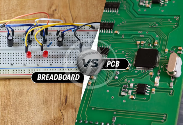
How Does Wave Soldering Differ from Reflow Soldering Process?
Wave soldering and reflow soldering process are two different manufacturing methods. Both create solder joints, but they suit different component types.
Wave soldering is mainly used for through-hole components. In this process, the bottom of the PCB passes over a wave of molten solder. The wave touches exposed leads and forms joints instantly. This method works best for connectors, pin headers, and large leaded devices.
Reflow soldering is used mainly for surface mount components. In this method, solder paste is printed first. Components sit on the paste. The assembly then heats inside a reflow oven until the paste melts.
Here are the major differences:
- Reflow soldering uses solder paste. Wave soldering uses molten solder waves.
- Reflow is ideal for SMT. Wave is ideal for through-hole.
- Reflow controls heat in multiple zones. Wave creates instant soldering in seconds.
- Reflow supports fine-pitch components. Wave is better for larger parts.
Both processes remain important. Many PCBs use mixed technology. In such cases, manufacturers combine reflow soldering for SMT components and wave soldering for through-hole components.
Which Reflow Soldering Defects Appear Most Often?
Several reflow soldering defects may occur if the process is not well controlled. However, with optimized temperature profiles and proper solder paste handling, these issues can be greatly reduced.
Here are the defects that appear most often:
- Tombstoning: One side of a small chip component lifts and stands upright. This occurs when pads heat unevenly.
- Bridging: Two adjacent pads connect accidentally with excess solder. This defect happens when too much solder paste is applied or components shift during heating.
- Insufficient Solder: There is not enough solder on a joint. This may result from poor paste printing or stencil wear.
- Voiding: Trapped gases inside the solder joint create small holes. While some voiding is normal, too much can weaken mechanical strength.
- Solder Balling: Small solder balls appear around pads. This defect often occurs when the paste splatters during reflow.
- Cold Joint: A joint looks dull or grainy. This happens when solder does not melt properly or cooling is inconsistent.
- Shifted Components: Components move out of position. Poor placement or low paste tackiness can cause this.
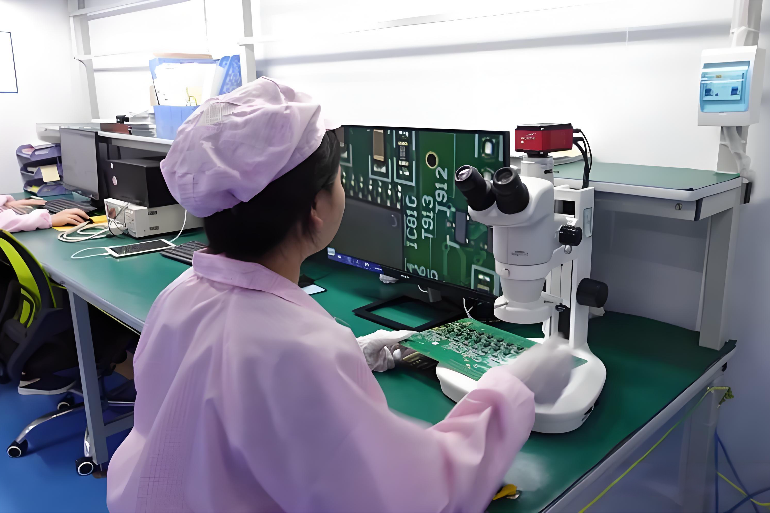
Modern reflow oven soldering process systems reduce most of these issues. Precise temperature control, optimized reflow soldering temperature profiles, and proper paste handling all help lower defect rates dramatically.
Why Is the SMT Reflow Soldering Process Used for Most PCBs?
The SMT reflow soldering process is used for most PCBs because it offers unmatched efficiency, precision, and reliability. It supports the fast pace of today’s electronics industry. It also fits the trend toward smaller, lighter, and more advanced products.
Several reasons make reflow the preferred choice:
- 1. High Accuracy
Reflow soldering offers excellent alignment and precise solder volume control.
- 2. High Productivity
Reflow ovens operate continuously. They handle large volumes with consistent performance.
- 3. Strong Mechanical Reliability
Reflow solder joints display strong bonding strength. They tolerate vibration, thermal cycling, and long-term use.
- 4. Supports Complex Boards
Modern multi-layer PCBs with complex designs rely on reflow soldering.
- 5. Wide Component Compatibility
Reflow supports everything from tiny resistors to large ICs. Its versatility is unmatched.
- 6. Lower Overall Cost
Automated reflow lines reduce labor cost and increase yield. This lowers total production cost.
- 7. Excellent Thermal Control
Reflow ovens regulate every degree of temperature. This precision protects sensitive devices during assembly.
Conclusion:
The reflow soldering process is the foundation of modern PCB assembly. It supports small components, dense designs, and advanced electronics. Each stage—from paste printing to cooling—plays a vital role in forming reliable joints.
With proper paste selection, precise thermal profiles, and excellent process control, the SMT reflow process delivers durable and consistent results across all industries.
If you need further help or want to discuss reflow soldering in more detail, feel free to reach out anytime at sales@bestpcbs.com