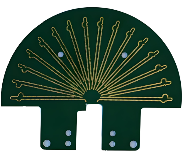
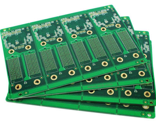
In EBest Circuit (Best Technology), the printed circuit Board manufacturing, particularly in high-frequency and high-speed signal transmission applications, Rogers Corporation’s PCB materials have become the go-to choice for our engineers. Rogers specializes in producing high-performance, highly reliable circuit board materials that find extensive use in wireless communications, automotive radar, satellite communication, and more. This blog post explores the unique advantages of Rogers PCBs and their significance in the international market.
What is Rogers PCB?
Rogers PCBs are renowned for their exceptional electrical performance. Compared to traditional FR-4 materials, Rogers materials offer a lower dissipation factor (Df), meaning they can maintain signal integrity at higher frequencies with reduced energy loss. This is critical for applications requiring precise data transmission such as 5G communications and millimeter-wave radars.
Rogers materials exhibit outstanding thermal stability. In high-temperature environments, these materials retain dimensional stability and mechanical strength, ensuring the reliability of PCBs under extreme conditions. For devices that need to operate stably over long periods, such as base stations or satellite communication equipment, this feature is especially important. Here is a comparison between Rogers materials and FR4.
Moreover, Rogers offers a range of materials with different characteristics to cater to various application needs. From low-loss to ultra-high-frequency applications, customers can choose the most suitable material based on their specific requirements. This not only enhances design flexibility but also provides more solutions to address complex engineering challenges.
In the context of globalization, competition in the international market has intensified. Utilizing Rogers PCB materials not only elevates the technical content and competitiveness of products but also offers customers a superior service experience. With the widespread adoption of 5G technology and the development of the Internet of Things (IoT), the demand for high-performance PCBs will continue to grow, making Rogers a leader in this field.
Advantages of Rogers PCB
1. Superior High-Frequency Performance
Rogers PCBs offer excellent electrical performance at high frequencies. Their stable dielectric constant and low loss tangent minimize signal loss and dispersion, which is critical for RF and microwave applications.
2. Low Dielectric Loss
Rogers materials have very low Df (dissipation factor), reducing power loss during signal transmission. This makes them highly efficient for high-speed, high-frequency signal paths.
3. Excellent Thermal Management
Rogers laminates have better thermal conductivity compared to standard FR4, allowing for more efficient heat dissipation. This helps maintain performance in demanding temperature environments.
4. Stable Electrical Properties
Their dielectric constant remains consistent over a wide range of temperatures and frequencies, enabling precise impedance control and signal integrity in advanced circuit designs.
5. Low Moisture Absorption
Rogers materials absorb less moisture than FR4, making them reliable for outdoor, aerospace, or high-humidity environments.
6. Better Reliability for Harsh Environments
With high temperature resistance and chemical stability, Rogers PCBs perform well in aerospace, military, and industrial applications where standard FR4 may fail.
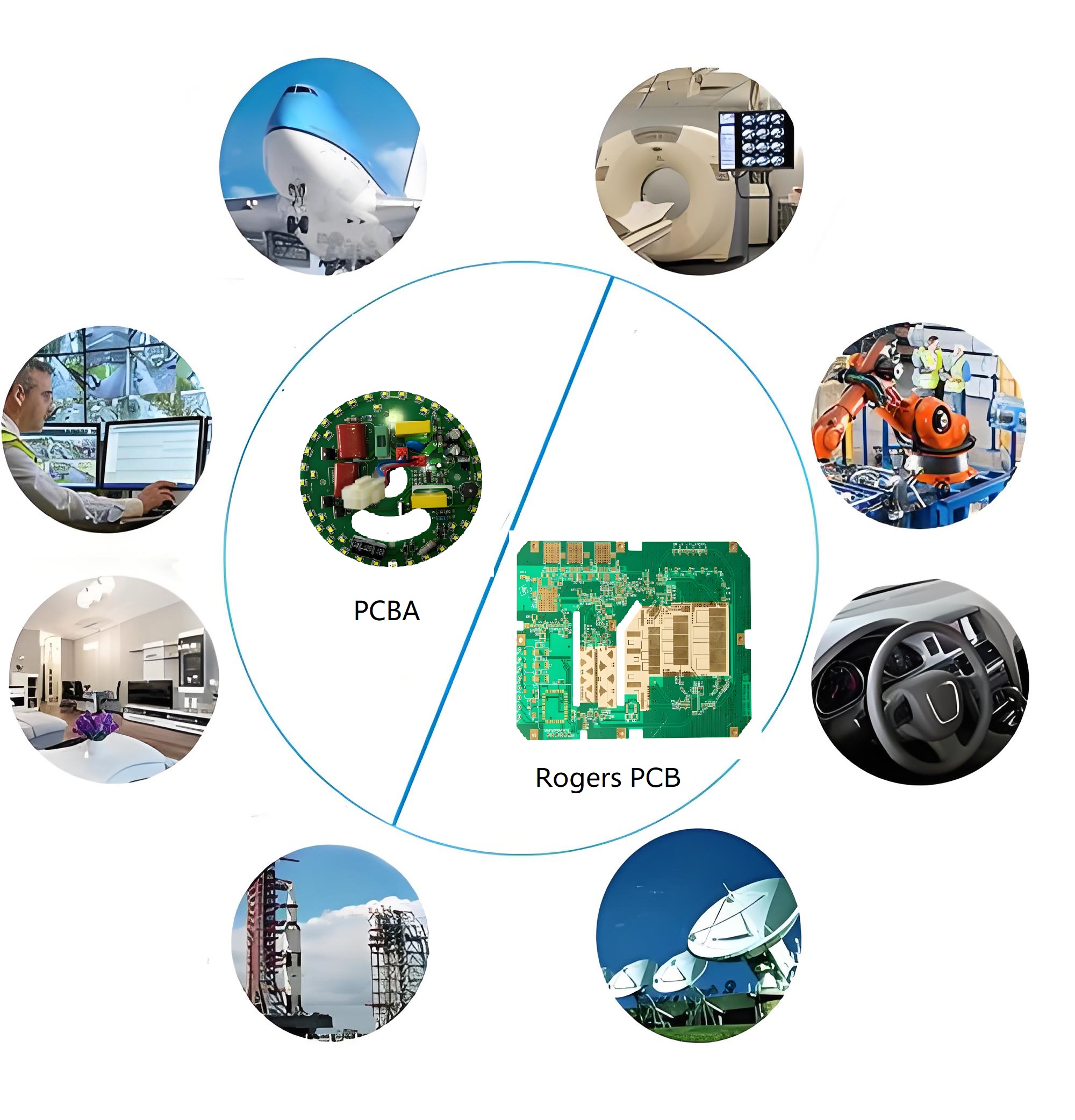
Applications of Rogers PCB
1. RF and Microwave Circuits
Rogers PCBs are widely used in radio frequency (RF) and microwave communication systems, including antenna arrays, radar modules, and RF amplifiers.
2. 5G Infrastructure
Due to their low signal loss and excellent high-frequency characteristics, Rogers boards are ideal for 5G base stations, antennas, and network hardware.
3. Aerospace and Defense Systems
In aviation, satellites, and military electronics, Rogers PCBs provide the precision and durability needed for mission-critical communication and control systems.
4. Automotive Radar and ADAS
Modern vehicles use Rogers-based PCBs in advanced driver assistance systems (ADAS), radar sensors, and collision avoidance modules for reliable performance under extreme conditions.
5. Medical Imaging and Equipment
Rogers boards are used in MRI machines, RF ablation devices, and other diagnostic tools where consistent signal performance is crucial.
6. High-Speed Digital Circuits
In computing and telecommunications, Rogers materials support high-speed signal integrity for backplanes, routers, and high-frequency data transmission boards.
Conclusion
Rogers PCBs stand out globally due to their outstanding performance and broad applicability. Whether developing new communication devices or improving existing systems, choosing Rogers is a wise decision. Their commitment to innovation ensures they remain at the forefront of technological advancement, providing unparalleled solutions for tomorrow’s electronic challenges.
Best Tech is a very professional manufacturer in printed circuit board. If you are interesting to know more information for Rogers PCB and other high-speed signal transmission application for printed circuit board, please come to contact us at any time.
Designing a reliable multilayer circuit board starts with getting the stackup right. If your project involves high-speed signals, compact layouts, or reduced EMI, an 8-layer PCB stackup is a solid choice. It offers flexibility, better performance, and room for complex routing.
In this guide, we’ll walk you through everything you need to know—layer configurations, materials, sizes, and how to make the most of this structure with the help of a trusted PCB manufacturer.
What is a PCB Stackup?
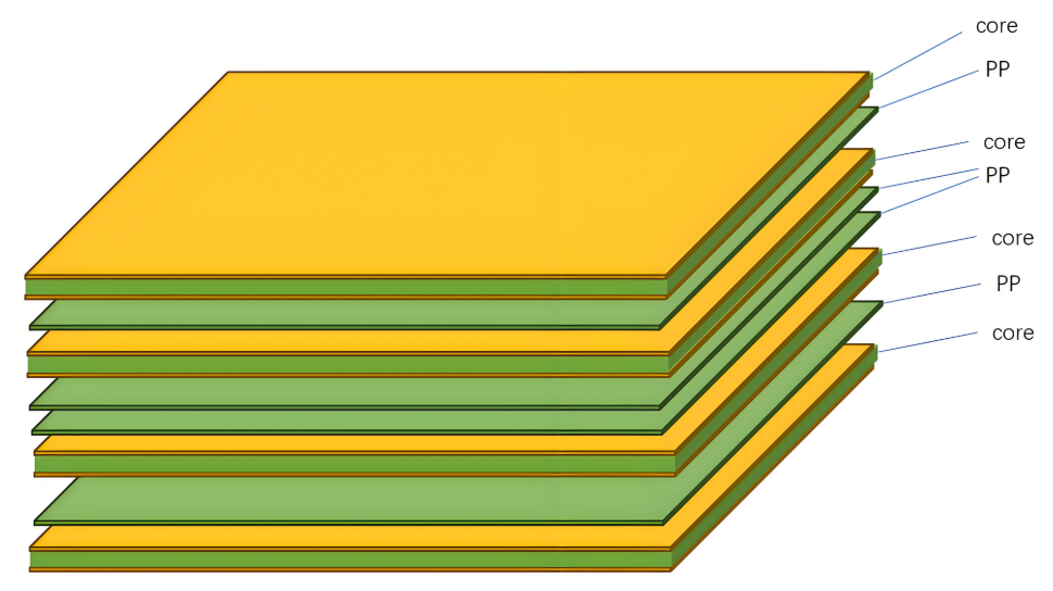
A PCB stackup is the arrangement of copper layers and insulating materials inside a circuit board. These layers are stacked and bonded together using prepreg (resin-impregnated fiberglass) and core materials. The goal is to create a reliable board that supports both mechanical strength and excellent electrical performance.
In simple words, the stackup decides how signal layers, power planes, and ground layers are placed in the board. In high-speed digital designs, this structure plays a big role in signal quality, electromagnetic compatibility (EMC), and overall performance.
For an 8-layer PCB, the stackup consists of eight layers of copper with alternating dielectric materials. These are usually divided into four signal layers and four plane layers, though that can change based on your design needs.
PCB Stackup Considerations
For most PCB designs, there are often competing requirements between electrical performance, manufacturing limitations, cost targets, and system complexity. The final PCB stackup is usually a result of careful trade-offs across these factors. High-speed digital circuits and RF systems commonly rely on multilayer boards for better control and performance. Below are 8 essential principles to consider when designing a reliable stackup:
1. Layer Arrangement
In multilayer PCBs, you’ll typically work with signal layers (S), power planes (P), and ground planes (GND). Power and ground planes are usually solid, unbroken areas that provide low-impedance return paths for signal currents. Signal layers are often positioned between these planes to form symmetrical or asymmetrical stripline structures. The top and bottom layers are mainly used for component placement and limited routing. It’s best to keep traces on these outer layers short to reduce direct radiation and EMI.
2. Defining a Single Power Reference Plane
Decoupling capacitors are vital for maintaining power integrity, and they can only be placed on the outer layers of the PCB. The trace length, pad design, and vias connected to these capacitors greatly affect their effectiveness. To improve decoupling, make these connections short and wide, and minimize via length. For example, in a high-speed digital system, place decoupling capacitors on the top layer, dedicate the second layer to power for the processor, use the third layer for signal routing, and assign the fourth layer as a ground reference.
3. Incorporating Multiple Ground Planes
Using multiple ground planes helps create low-impedance return paths and minimizes common-mode EMI. Ground and power planes should be tightly coupled, and signal layers should also be close to reference planes. Reducing the dielectric thickness between layers improves coupling and enhances performance.
4. Managing Multiple Power Planes
When your design includes more than one power plane, these planes are often split into different voltage regions. If a signal layer is placed next to a multi-region power layer, signal currents may not find clean return paths, leading to noise or EMC issues. For high-speed digital signals, avoid routing traces near split power planes to prevent return current discontinuities.
5. Designing Signal Routing Pairs
When a signal travels from one layer to another, it creates what’s known as a “routing pair.” Ideally, the return current should stay within the same reference plane when switching layers. In practice, however, signals often need to transition between layers. To maintain signal integrity, ensure that return paths are available through stitching vias or decoupling capacitors. Using adjacent layers as routing pairs is a practical and effective strategy.
6. Routing Direction Guidelines
Keep trace directions consistent within each signal layer. At the same time, rotate the routing direction between adjacent signal layers. For instance, use horizontal routing (X-axis) on one layer and vertical routing (Y-axis) on the next. This practice reduces crosstalk and improves signal clarity.
7. Even-Layer Designs is Better
Although odd-layer PCBs may appear cheaper due to fewer materials, they’re more expensive to manufacture. That’s because odd-layer boards require non-standard lamination processes and additional handling steps. These increase the risk of surface damage, incorrect etching, and longer production times. In contrast, even-layer PCBs are more stable, cost-effective, and easier to produce at scale.
8. Budget
Multilayer PCBs are naturally more expensive than single- or double-layer boards. However, they offer significant benefits in functionality, miniaturization, EMI control, and signal integrity. When weighing total cost versus performance, the difference between multilayer and simpler boards may not be as high as expected.
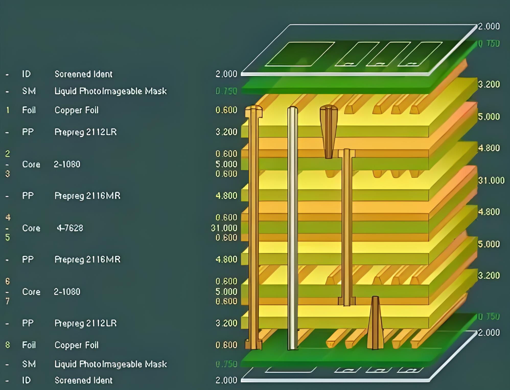
Standard 8-Layer PCB Stackup Structure
When it comes to multilayer PCB design, the arrangement of signal, power, and ground layers directly affects signal integrity, EMI performance, and power delivery. Below are three common 8-layer stackup configurations, each with its own strengths and limitations.
Option 1:
Layer 1: Signal 1
Layer 2: Signal 2
Layer 3: Ground
Layer 4: Signal 3
Layer 5: Signal 4
Layer 6: Power
Layer 7: Signal 5
Layer 8: Signal 6
This layout alternates signal and power layers but does not take full advantage of the electromagnetic shielding benefits that a multilayer board can offer. The ground and power planes are separated, reducing the board’s EMI suppression capability. In addition, the power distribution network suffers from higher impedance, which may affect voltage stability in high-speed or high-current applications.
Option 2:
Layer 1: Signal 1
Layer 2: Ground
Layer 3: Signal 2
Layer 4: Power
Layer 5: Ground
Layer 6: Signal 3
Layer 7: Ground
Layer 8: Signal 4
This structure is widely regarded as the optimal 8-layer PCB stackup. It provides excellent electromagnetic shielding through the use of multiple ground planes. Each signal layer is placed adjacent to a reference plane (either ground or power), which improves signal stability and impedance control. Additionally, the tight coupling between power and ground planes enhances EMI performance and power integrity. This setup is ideal for high-speed, high-frequency, or noise-sensitive applications.
Option 3:
Layer 1: Signal 1
Layer 2: Ground
Layer 3: Signal 2
Layer 4: Power
Layer 5: Ground
Layer 6: Signal 3
Layer 7: Power
Layer 8: Signal 4
This configuration is a variation of Option 1 with improved EMI performance. By adding an extra reference plane, it provides better control over the characteristic impedance of the signal layers. However, the placement of the second power plane (with limited coupling to a nearby ground) leads to higher power delivery impedance, which could be a drawback in power-sensitive designs. Some optimization in power layer arrangement is still needed.
8-Layer PCB Stackup Materials
The performance of an 8-layer PCB stackup relies heavily on the materials used between and around its copper layers. These materials affect everything from electrical behavior to thermal stability and even mechanical strength. Let’s look at the two main categories: conductive and dielectric materials.
1. Conductive Layers
Copper is the most common metal used for the conductive layers in an 8-layer PCB. It’s highly conductive, easy to work with, and available in different thicknesses and finishes.
Copper Thickness: Most boards use ½ oz or 1 oz copper per layer. If the design needs to handle higher current, 2 oz or thicker copper may be used.
Copper Type: Standard copper foil is either electrodeposited (ED) or rolled. Rolled and annealed copper is smoother and more flexible, which makes it useful in boards that need better bend resistance.
Surface Finishes: The exposed copper is usually treated with a surface finish to protect it and ensure solderability. Options include HASL, ENIG, OSP, and immersion silver, among others.
2. Dielectric Layers
The dielectric materials are the insulating layers that separate the copper traces. These layers are critical for controlling impedance, heat flow, and electrical isolation.
FR-4: A glass-reinforced epoxy laminate, FR-4 is the most common dielectric for general-purpose PCBs. It’s reliable, widely available, and cost-effective.
High-Frequency Materials: For RF and high-speed digital designs, materials with low dielectric loss—like PTFE (Teflon), ceramic-filled PTFE, or hydrocarbon-based ceramics—are preferred. These support better signal integrity at high frequencies.
Thermal Conductive Materials: When heat dissipation is a concern, substrates like alumina or aluminum nitride are used. These materials offer higher thermal conductivity than standard epoxy systems.
To hold everything together, manufacturers use prepregs—uncured fiberglass sheets soaked in resin. Common prepreg materials include FR-4 for standard designs and polyimide for higher thermal or mechanical stress environments.
At the center of the stackup is the core, which acts like a spine for the board. This rigid layer typically uses FR-4 or polyimide, though in some high-power or high-heat applications, metal cores are added to improve thermal performance.
8-Layer PCB Thickness & Sizes
The total thickness of an 8-layer PCB depends on several factors:
Copper thickness: Common values are 0.5oz, 1oz, or 2oz per layer.
Prepreg/Core thickness: Adjusted to achieve specific impedance and board height.
Number of plane vs signal layers: Affects thermal and mechanical behavior.
Common Thickness Options:
1.6mm (0.063″) – Industry standard, suitable for most applications.
2.0mm to 2.4mm – Used when extra copper is needed for higher current.
3.2mm or custom – Selected for industrial or military-grade boards.
PCB Sizes:
Panel sizes are typically 18” x 24” before routing. Your board can be as small as a few millimeters or as large as the full panel, depending on the application.
6 Layer vs 8 Layer PCB
A 6-layer PCB consists of six layers of copper circuitry stacked with insulating layers (prepreg and core) in between. It usually includes:
4 Signal Layers for routing high- and low-speed signals
1 Power Plane to distribute voltage
1 Ground Plane to provide a return path and help with EMI suppression
A typical 6-layer stackup looks like this:
Layer 1: Signal (Top)
Layer 2: Ground
Layer 3: Signal
Layer 4: Signal
Layer 5: Power
Layer 6: Signal (Bottom)
While both 6-layer and 8-layer PCBs are widely used in advanced electronics, they serve slightly different purposes depending on design complexity, signal speed, and EMI requirements. Let’s compare them together:
Aspect
6-Layer PCB
8-Layer PCB
Layer Count
6
8
Typical Configuration
4 signal layers + 1 power + 1 ground
4 signal layers + 2 power + 2 ground
Routing Space
Moderate
More routing room
Signal Integrity
Good, suitable for most mid-speed signals
Excellent, supports very high-speed signal routing
EMI Shielding
Limited shielding with fewer ground planes
Strong EMI control due to multiple ground planes
Power Distribution
Single power plane, higher impedance
Dual power planes, better PDN performance
Design Complexity
Less complex, easier to design and fabricate
More complex, better for advanced designs
Thermal Performance
Adequate for medium power applications
Better heat spreading for high-power components
Cost
Lower fabrication cost
Higher cost due to more layers and materials
Use Case
Mid-level MCUs, general embedded, basic RF
FPGAs, DDR memory, high-speed data buses, complex SoCs
Use a 6-Layer PCB if:
Your design isn’t extremely dense.
The signals don’t require tight EMI control.
You want to balance performance and cost.
There’s no strict need for multiple ground or power planes.
It’s widely used in commercial electronics that don’t involve ultra-high-speed communication or compact multilayer routing challenges.
Choose an 8-Layer PCB when:
High-speed signals (such as PCIe, USB 3.x, DDR4, or SERDES) are involved.
EMI performance is critical, especially in sensitive industrial or medical devices.
You need more space for routing due to a denser component layout.
Stable power delivery is required across multiple voltage domains.
You’re working with a compact form factor that demands vertical signal distribution.
An 8-layer stackup allows designers to pair every signal layer with a nearby ground or power plane, which significantly improves signal quality and reduces noise.
Benefits of Working with an Experienced PCB Manufacturer
Designing and fabricating an 8-layer PCB stackup requires precise engineering and process control. Partnering with a reliable manufacturer like EBest Circuit (Best Technology) brings several benefits:
1. Stackup Design Assistance: Professional help with impedance control, signal integrity, and EMC optimization.
2. Material Expertise: Guidance in choosing suitable laminates for your specific requirements.
3. Advanced Fabrication: Capability to handle HDI, blind/buried vias, and tight tolerances.
4. Quality Assurance: Rigorous testing like AOI, X-ray, and impedance measurement.
5. Fast Turnaround: Efficient production process without sacrificing quality.
Why Choose EBest Circuit (Best Technology) for Your 8-Layer PCB Stackup?
EBest Circuit (Best Technology) is a trusted 8-layer PCB stackup specialist serving global customers across aerospace, medical, automotive, and industrial electronics. We hold certifications including:
ISO9001 for quality control
ISO13485 for medical electronics
IATF16949 for automotive-grade PCBs
AS9100D for aerospace applications
Our engineers assist with DFM check, impedance control, EMI reduction, thermal management, and material choices, ensuring your 8-layer design performs reliably under real-world conditions.
FAQs
1. What is the best layer configuration for an 8-layer PCB stackup?
A balanced configuration like Signal–GND–Signal–Power–GND–Signal–Power–Signal is often preferred for signal integrity and EMI control.
2. How much does an 8-layer PCB cost?
Cost varies by material, size, copper weight, and complexity, but typically ranges from $50 to $300 per board in small batches.
3. What software is used for 8-layer PCB design?
Tools like Altium Designer, Eagle, KiCAD, and OrCAD support multilayer PCB stackup planning and layout.
4. Can you use HDI features in 8-layer PCBs?
Yes. Blind and buried vias, via-in-pad, and microvias are often used in 8-layer HDI designs.
5. How do I choose the right manufacturer for 8-layer PCBs?
Look for certifications, material options, engineering support, and experience with multilayer stackups—like what EBest Circuit (Best Technology) provides.
Rogers RO4350B is one of the most popular PCB materials used in high-frequency applications today. If you’re designing circuits that need stable performance at GHz-level speeds, this material often stands out. In this blog, we’ll explore what RO4350B is, what it’s made of, available thicknesses, and why it’s preferred over other materials for high-frequency PCB designs.
What Is Rogers RO4350B Material?
RO4350B is a type of high-frequency laminate developed by Rogers Corporation. It’s engineered for performance in RF (radio frequency) and microwave applications, offering superior electrical characteristics compared to standard FR-4. Unlike generic epoxy-based materials, RO4350B uses a hydrocarbon-ceramic composition that keeps signal losses low even at high frequencies.
This material combines the electrical performance of PTFE (commonly used in high-end RF applications) with the manufacturability of FR-4, making it a cost-effective and reliable choice for high-speed designs.
What Is Rogers Material Made of?
Rogers materials, including RO4350B, are made from hydrocarbon resins with ceramic fillers and reinforced with woven glass. This composite structure delivers excellent mechanical stability and consistent dielectric properties.
Unlike traditional PTFE-based laminates, Rogers materials like RO4350B do not require special handling during PCB fabrication, which saves both time and cost. Rogers materials are engineered to balance electrical performance with ease of manufacturing, which is essential when producing high-frequency PCBs at scale.
RO4350B Dielectric Constant
The dielectric constant (Dk) is a critical factor in high-frequency PCB materials, as it affects signal speed and impedance control. The RO4350B dielectric constant is typically 3.48 ± 0.05 at 10GHz, which is both stable and predictable over a wide range of frequencies and temperatures.
The consistency of frequencies and temperatures ensure that transmission lines behave as expected, which is especially important in RF circuits, microwave devices, and antenna structures. Stable Dk also simplifies impedance control and reduces the risk of signal reflection and distortion.
What Is the Standard RO4350B Thickness?
RO4350B PCBs are available in multiple standard thicknesses to meet different design and performance requirements. Common options include:
0.254 mm (10 mil)
0.508 mm (20 mil)
0.762 mm (30 mil)
1.524 mm (60 mil)
These thicknesses allow designers to select the best stack-up for impedance control, thermal dissipation, and mechanical strength. Depending on your signal layer, ground layer spacing, or copper weight, one of these thicknesses will likely align with your project’s needs.
RO4350B Datasheet
Before choosing a material for your RF or high-speed digital PCB, it’s essential to understand the technical specifications. Here is a summary of the most important values from the RO4350B datasheet:
Property
Typical Value
Test Condition / Note
Dielectric Constant (Dk)
3.48 ± 0.05
@ 10 GHz (z-axis)
Dissipation Factor (Df)
0.0037
@ 10 GHz
Volume Resistivity
1.7 × 10⁸ MΩ·cm
ASTM D257
Surface Resistivity
4.4 × 10⁷ MΩ
ASTM D257
Electrical Strength
>800 V/mil
ASTM D149
Dielectric Breakdown
>40 kV
ASTM D149
Thermal Conductivity
0.69 W/m·K
ASTM D5470
Coefficient of Thermal Expansion (CTE)
11 ppm/°C (x, y) / 32 ppm/°C (z)
-55°C to 288°C
Glass Transition Temperature (Tg)
>280°C (no defined Tg)
Thermomechanical analysis
Decomposition Temperature (Td)
~425°C
TGA method
Solder Reflow Resistance
Excellent
No delamination or blistering
Tensile Modulus
1.4 × 10⁶ psi (x-y)
ASTM D638
Flexural Strength
20,000 psi (typical)
ASTM D790
Peel Strength
≥1.1 N/mm
IPC-TM-650
Young’s Modulus
~10 GPa
Estimated from stress-strain curve
Moisture Absorption
0.06%
ASTM D570
Density
1.86 g/cm³
ASTM D792
Flammability Rating
UL 94 V-0
UL 94
Water Absorption
<0.1%
Excellent water resistance
Material Composition
Ceramic-filled hydrocarbon resin + glass fiber
Non-PTFE-based
Halogen-Free
Yes
RoHS & REACH compliant
Available Copper Foil
0.5 oz, 1 oz, 2 oz (18µm, 35µm, 70µm)
Rolled and electro-deposited options available
If you need the full official datasheet in PDF format, you can also request it from EBest Circuit (Best Technology) along with a quote for your project.
How Much Does Rogers PCB Cost?
Compared to FR-4, the rogers RO4350B price is higher due to its premium performance. On average, RO4350B material can cost between $8 to $25 per square foot, depending on thickness, copper weight, and supplier volume. Full PCB fabrication using RO4350B typically results in a 20–50% higher price than using standard FR-4, mainly due to the material cost and additional processing steps.
However, when you’re working with high-frequency applications—such as 5G, radar, or satellite communications—the improved signal integrity and reduced loss often justify the added cost.
What Is the Difference Between RO4003 and RO4350B?
Both RO4003 and RO4350B are part of Rogers’ high-frequency laminate series, but they have subtle differences:
Feature
RO4003C
RO4350B
Dielectric Constant
3.38
3.48
Loss Tangent
0.0027 @ 10 GHz
0.0037 @ 10 GHz
Flame Rating
Non-UL rated
UL 94 V-0
Cost
Slightly lower
Slightly higher
Process Compatibility
Standard PCB process
Standard PCB process
RO4003 is better suited for applications where cost sensitivity is critical and UL rating is not required. RO4350B, on the other hand, provides a better flame rating and slightly improved mechanical properties, so it is the preferred choice for commercial or defense-grade applications.
Why Choose RO4350B as High Frequency PCB Material?
High frequency PCB, also known as RF PCB, refers to a special circuit boards with relatively high electromagnetic frequencies. This PCB is mainly used in the fields of high frequency (>300 MHz or wavelengths <=1 meter) and microwaves (>3 GHz or wavelengths <= 0.1 meter). If you’re designing a high-frequency PCB, choosing RO4350B gives you the best of both worlds: high performance and ease of fabrication. Here’s why many engineers choose this material:
Low dielectric loss helps reduce signal attenuation.
UL 94 V-0 flame resistance, which is crucial for safety.
Compatible with standard FR-4 processing, so no need for Teflon-specific tooling.
All of these feature help maintain signal quality in applications like RF transmitters, satellite receivers, and high-speed digital circuits. So even if the RO4350B price is slightly higher, it’s often more cost-effective than debugging performance issues caused by suboptimal materials.
High Frequency PCB Design Guidelines
When working with RO4350B PCB material, keep the following design practices in mind to get the best results:
1. Control impedance: Use proper stack-up and trace width calculators for accurate 50Ω or 75Ω routing.
2. Minimize vias: Each via introduces inductance and can distort signals at high frequencies.
3. Short trace lengths: High-speed signals should have the shortest possible paths.
4. Proper grounding: Always include a continuous ground plane to reduce EMI and improve return paths.
5. Avoid sharp corners: Use 45-degree or curved traces instead of 90-degree angles.
6. Use differential pairs: For high-speed interfaces like USB or LVDS, tightly coupled pairs reduce crosstalk and maintain signal integrity.
Combining these techniques with the natural performance of RO4350B helps you unlock superior RF performance without increasing fabrication complexity.
Why EBest Circuit (Best Technology) Is Your Reliable RF PCB Manufacturer?
At EBest Circuit (Best Technology), we specialize in high-frequency PCB manufacturing using premium materials like RO4350B, RO5880, RO4003C. With ISO-certifications, we’re equipped to serve industries ranging from automotive and medical to aerospace and communications. Whether you’re developing high-reliability prototypes or large-scale production, you can count on us as your reliable one-stop PCB & PCBA partner.
We offer:
Strict impedance control with advanced test equipment
Rapid prototyping and flexible volume production
Competitive RO4350B price with guaranteed traceability
Expert engineering support for layout and material selection
No MOQ requires, 1 piece available also
5 years quality guarantee, free rework and functional testing
Free DFM check
If you’re looking to manufacture reliable high-frequency PCBs, you’re in the right place.
FAQs
1. Is RO4350B suitable for multilayer PCBs?
Yes, RO4350B is commonly used in multilayer designs for RF and microwave applications. It offers stable performance in both single and multi-layer stack-ups.
2. How does RO4350B perform at 5GHz or higher?
It maintains low loss and consistent Dk values even at frequencies above 5GHz, making it reliable for 5G and radar circuits.
3. Can RO4350B be used with FR-4 in hybrid stack-ups?
Yes, it can. Many engineers use RO4350B for RF layers and FR-4 for power/control layers to reduce cost.
4. What is the shelf life of RO4350B material?
Stored under proper conditions, it has a long shelf life—typically over a year without degradation.
5. Do I need special PCB fabrication for RO4350B?
No. Unlike PTFE-based materials, RO4350B is compatible with standard PCB fabrication processes, which simplifies manufacturing.
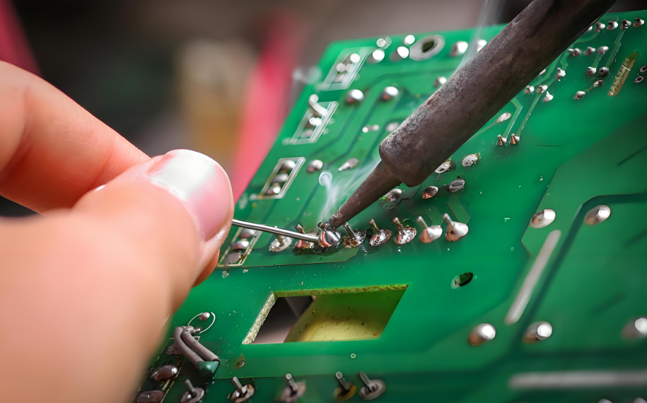
The typical solder temperature for PCBs is 240℃ to 270℃ for lead-free soldering, and 240℃to 260℃ for lead-based soldering.
If you’re building or repairing a PCB, knowing the right soldering temperature is key. It keeps your components safe and ensures strong connections. The temperature you use depends on the type of solder and the method. In this blog, we’ll break down everything you need to know about solder temperatures for PCBs.
Why Solder Temperature Matters in PCB Work?
When working with printed circuit boards, one of the most critical factors for quality and reliability is soldering temperature. Whether you’re assembling prototypes, repairing a PCB, or managing high-volume production, knowing the right temperature is essential for success.
Too low, and the solder won’t melt properly. Too high, and you might damage the board or components. Accurate temperature helps create reliable joints and avoids costly rework. It also protects sensitive parts from overheating.
Solder temperature affects not only how well the joints form but also how long your product will last in real-world use. In this blog, we’ll explore the ideal soldering temperatures for different solders and methods—and how to avoid costly mistakes.
What Determines Soldering Temperature?
Soldering temperature is not a fixed value. It depends on several key factors:
Type of solder alloy (leaded or lead-free)
Soldering process (manual, reflow, wave)
PCB material (standard FR-4, high-Tg, ceramic, etc.)
Component sensitivity
Ambient factory temperature and humidity
Each variable impacts how heat should be applied to the board. Applying the right temperature at the right time ensures the best wetting, strong mechanical bonds, and excellent electrical contact.
Solder Types and Their Melting Temperatures
Lead-Based Solder (e.g., Sn63/Pb37)
Melting point: 183°C
Typical working temperature: 240°C to 260°C
Benefits: Good wetting, lower processing temperature
Drawbacks: Contains lead; banned in many consumer products (RoHS compliance)
Lead-based solder is often used in military, aerospace, or industrial environments where reliability outweighs regulatory restrictions. It’s easier to work with and provides strong joints with less thermal stress on components.
Lead-free solder has become the standard in modern electronics manufacturing due to environmental regulations. However, it requires precise control of temperature and time to ensure quality results.
Soldering Methods and Their Temperature Profiles
Let’s explore how soldering temperatures vary across different processes used in PCB manufacturing and assembly.
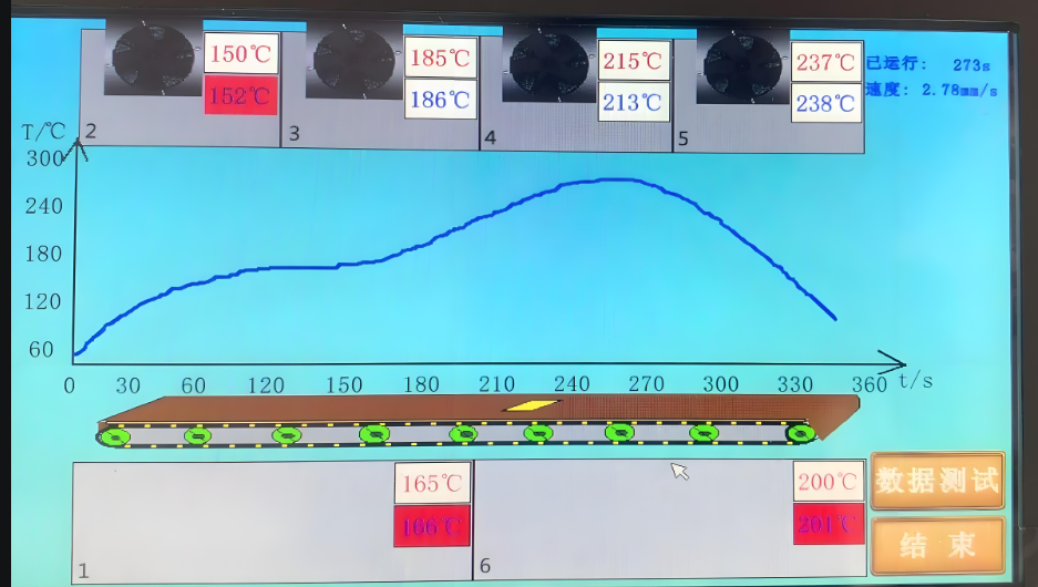
1. Reflow Soldering
Reflow soldering is the most common method for assembling surface-mount components. A solder paste (a mix of powdered solder and flux) is applied to the PCB, and components are placed on top. Then, the board goes through a reflow oven with controlled temperature zones.
Reflow Temperature Profile (Lead-Free):
Preheat: 150°C–180°C for 60–120 seconds
Soak: 180°C–200°C for 60–90 seconds
Reflow Peak: 240°C–250°C for 30–60 seconds
Cool-down: Controlled descent to room temperature
Reflow Temperature Profile (Lead-Based):
Preheat: 120°C–150°C
Soak: 150°C–180°C
Reflow Peak: 210°C–230°C
Cool-down: Gradual cooling to avoid thermal shock
The peak temperature should not exceed the maximum rating of components, and the time above liquidus (TAL) must be kept short to avoid damaging the board.
2. Wave Soldering
Wave soldering is widely used for through-hole assemblies and some mixed-technology PCBs. The board passes over a wave of molten solder.
Lead-Based Solder: 245°C–255°C
Lead-Free Solder: 260°C–270°C
Before reaching the solder wave, the PCB is preheated to about 100°C–150°C to prevent thermal shock and improve solder wetting. Flux is applied before the preheat stage to clean and prepare pads.
3. Hand Soldering
Hand soldering is still widely used in prototyping, repair work, or in low-volume custom assemblies. It uses a soldering iron with a temperature-controlled tip. Recommended tip temperatures:
Lead-Based Solder: 330°C to 370°C
Lead-Free Solder: 350°C to 400°C
While this may seem high, actual contact time is very short (1–3 seconds). A good soldering station will allow precise control and thermal recovery. Operators must avoid overheating pads or components.
Does the PCB Material Affect Soldering Temperature?
Yes—PCB material plays a major role in how much heat it can tolerate.
FR-4 (Standard)
Can handle up to 260°C for short durations
Common for most consumer and industrial PCBs
High-Tg FR-4
Higher glass transition temperature (Tg ~170°C to 180°C)
More stable under high thermal stress
Ideal for lead-free soldering or multilayer boards
Ceramic PCBs (Alumina, Aluminum Nitride)
Extremely high thermal stability
Can endure 300°C+ without damage
Requires more precise soldering to avoid cracking
Metal Core PCBs (Aluminum, Copper Core PCB)
Withstand up to 260°C for short durations
High thermal conductivity due to the metal core
Used in: Power electronics, lighting, and automotive control
Aluminum boards dissipate heat quickly, which helps during soldering. However, the uneven expansion between the metal and dielectric layer requires careful control to avoid mechanical stress during reflow.
Flex Circuits (Flexible PCBs)
Max soldering temperature: Typically <250°C
Material: Polyimide or PET base
Critical risk: Heat can distort, shrink, or damage traces
Flexible PCBs are more heat-sensitive than rigid boards. The polyimide or PET base can tolerate soldering but has lower thermal mass, which means it heats up—and cools down—faster. Excessive temperature or contact time can easily cause:
Wrinkling or warping
Delamination of copper traces
Tearing at bend areas
When soldering flex circuits:
Use lower reflow peak temperatures, typically not exceeding 240°C–245°C.
Apply thermal barriers or stiffeners in vulnerable areas.
Ensure the heating and cooling are gradual to prevent mechanical stress.
Flex PCBs often use selective soldering or low-temperature solders to reduce heat exposure. In some cases, hot-bar soldering or laser soldering is used for better temperature precision.
At EBest Circuit (Best Technology), we ensure every PCB assembly follows strict soldering standards. Our team uses professional thermal profiling tools to fine-tune the temperature curve for each product.
We support:
RoHS-compliant lead-free soldering
Lead-based solder for specialized industries
High-Tg and ceramic PCBs
Automated reflow and wave soldering
Manual soldering by IPC-trained operators
Suppose you have any questions about our products and service, price, MOQ, delivery, location, quality standards, certificates, engineering support and so on. We offer engineering support, thermal profiling, and high-quality PCB manufacturing for all your assembly needs. Please contact us freely any time. We aim to be the best PCB manufacturers in China to supply our customers with the best quality, price, and services. Contact us right now to discuss your next PCB project or to request a quote!
FAQs
1. What is the ideal soldering temperature for lead-free solder?
A peak reflow temperature of 245°C–250°C is typical. Manual soldering may require a tip temp of 350°C–370°C.
2. Can I use the same temperature for leaded and lead-free solder?
No. Lead-free solder needs a higher temperature due to its higher melting point.
3. Will high soldering temperatures damage my PCB?
If temperatures are too high or sustained too long, they can cause delamination, burnt pads, or component failure. Use proper profiling.
4. What’s the difference between peak temperature and tip temperature?
Peak temperature is the highest board temp during reflow. Tip temperature is the iron’s surface heat during manual soldering.
5. How can EBest Circuit (Best Technology) help with soldering specifications?
We provide detailed thermal profiles, component-safe soldering, and high-reliability assembly for all PCB types.
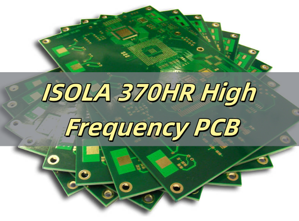
Isola 370HR is a well-established choice for engineers who need a durable, high-frequency compatible PCB base material. Its high Tg, low loss, and excellent reliability make it suitable for everything from aerospace to telecommunications.
If you’re working on a complex design or RF application, switching to Isola 370HR PCB materials might be the upgrade you need. And with a reliable partner like EBest Circuit (Best Technology), you’re assured of quality from the first prototype to volume production.
What Is Isola 370HR Material?
Isola 370HR is a high-performance, high-Tg epoxy laminate and prepreg system developed by Isola Group. Designed specifically for multilayer printed circuit boards, it offers a great balance between electrical stability and thermal durability. It’s classified as a high-Tg FR4 material but provides better signal handling and thermal behavior compared to standard FR4.
Isola engineered this material for demanding sectors like telecommunications, data networking, and military electronics. Its low dielectric loss and stable performance across a wide frequency range make it suitable for modern high-speed circuits.
Advantages of Using Isola 370HR in PCB Manufacturing
Choosing Isola 370HR for your PCB manufacturing brings several key benefits that directly impact the performance and reliability of your finished products:
Superior Thermal Stability: With a high glass transition temperature (~180°C), Isola 370HR withstands the high temperatures of lead-free soldering and multiple reflow cycles without warping or delamination.
Low Dielectric Loss: This material minimizes signal loss at high frequencies, making it perfect for RF circuits and high-speed digital designs.
Excellent Signal Integrity: Stable dielectric constant (Dk) across frequency ranges means consistent signal propagation and reduced timing errors.
Enhanced Moisture and CAF Resistance: Improved resistance to moisture-induced failures helps maintain long-term reliability, especially in humid or harsh environments.
Dimensional Stability: Reduced Z-axis expansion ensures layers stay aligned during manufacturing and operation, critical for multilayer PCBs.
IPC Compliance: Isola 370HR meets rigorous industry standards, ensuring compatibility with demanding aerospace, automotive, and medical applications.
RoHS and Environmental Compliance: Fully compliant with environmental regulations, supporting green manufacturing practices.
ISOLA 370HR Datasheet
Property
Typical Value
Test Method / Notes
Glass Transition Temperature (Tg)
180°C (DSC)
Differential Scanning Calorimetry
Decomposition Temperature (Td)
>340°C
TGA (Thermogravimetric Analysis)
Dielectric Constant (Dk)
4.04 @ 1 GHz
IPC-TM-650 2.5.5.5
Dissipation Factor (Df)
0.0127 @ 1 GHz
IPC-TM-650 2.5.5.5
Coefficient of Thermal Expansion (CTE)
15 ppm/°C (X-Y), 65 ppm/°C (Z)
IPC-TM-650 2.4.24
Thermal Conductivity
0.4 W/m·K
ASTM E1461
Tensile Strength
24,000 psi
IPC-TM-650 2.4.18
Flexural Strength
32,000 psi
IPC-TM-650 2.4.4
Water Absorption
<0.10%
IPC-TM-650 2.6.2.1
Flammability Rating
UL 94 V-0
UL 94
Copper Peel Strength
>1.0 lbs/inch
IPC-TM-650 2.4.8
Surface Resistivity
>1×10^6 ohms
ASTM D257
Volume Resistivity
>1×10^9 ohm-cm
ASTM D257
Dielectric Breakdown Voltage
>50 kV/mm
IPC-TM-650 2.5.6
What Is the Difference Between FR4 and 370HR?
While both standard FR4 and Isola 370HR are epoxy-based materials widely used in PCB manufacturing, they differ significantly in performance—especially when it comes to high-speed and high-frequency applications.
Standard FR4 is the go-to material for many general-purpose PCBs. It offers decent mechanical strength, good manufacturability, and cost-effectiveness for everyday electronics. However, its glass transition temperature (Tg) typically ranges from 130°C to 140°C, and it has relatively higher dielectric loss (Df). These limitations can cause signal degradation and reliability issues in circuits operating at higher frequencies or elevated temperatures.
In contrast, Isola 370HR is a high-Tg FR4 variant designed to meet the demands of more challenging environments. Its Tg is around 180°C, which provides superior thermal stability during lead-free soldering and extended use in high-temperature settings. More importantly, it exhibits a lower dielectric constant (Dk) and dissipation factor (Df), which translates to lower signal loss and better signal integrity at microwave and radio frequencies.
Why Isola 370HR PCBs Are Suitable for High Frequency Applications?
As electronic devices evolve to support faster data rates, the performance of PCB materials under high-frequency conditions has become a serious concern. This is where Isola 370HR PCB materials shine.
Its consistent dielectric constant (Dk) and low dissipation factor (Df) ensure that high-frequency signals do not lose strength or become distorted. That’s a major reason why 370HR is used in:
Gigabit Ethernet systems
High-speed backplanes
Automotive radar systems
Satellite communications
Advanced test equipment
Its ability to handle GHz-level signals without distortion helps maintain data accuracy and reduces EMI-related issues.
When to Choose Isola 370HR Material for Your PCB?
You might consider Isola 370HR when your design falls into any of the following categories:
High-speed or RF designs: If your circuit runs at over 1 GHz, this material can preserve signal quality.
Multilayer PCBs: When stacking 8 or more layers, 370HR offers great registration control and stability.
Thermal stress tolerance: It performs reliably through multiple reflow cycles and temperature extremes.
CAF-resistant needs: Ideal for products exposed to moisture or long-term outdoor use.
Strict industry compliance: It meets IPC-4101/126 and 129, as well as UL and RoHS requirements.
Choosing this material isn’t just about performance—it’s about peace of mind over the product’s lifecycle.
How to Identify Genuine Isola 370HR PCB Material?
To avoid counterfeit materials or unverified substitutions, it’s important to:
Request the original datasheet with the Isola logo and batch number.
Check board markings for Isola brand identification or laminate codes.
Work with certified suppliers who purchase directly from Isola or its authorized distributors.
Ask for certification documents, especially if your application is regulated by aerospace or medical standards.
Genuine Isola 370HR PCB materials ensure consistency in production and performance.
Typical Applications of Isola 370HR in PCB Design
Here are common industries and devices where Isola 370HR is frequently used:
Telecommunications: High-speed switches, routers, and fiber optic systems.
Aerospace and Defense: Radar, avionics, satellite boards.
Medical Equipment: Imaging devices, patient monitoring systems.
Automotive: Advanced driver-assistance systems (ADAS), LiDAR modules.
Industrial Automation: Motor controls, power management systems.
Designers across these sectors rely on its thermal reliability and signal control to reduce field failures.
What Is the Equivalent of Isola 370HR?
While Isola 370HR is a preferred material, there are other options that offer similar characteristics. Here’s how some alternatives compare:
Material Name
Tg (°C)
Df @ 1GHz
Notable Feature
Nelco N4000-13EP
~180
~0.013
Known for stability
Panasonic MEGTRON 6
~185
~0.0025
Ultra-low loss, but expensive
Ventec VT-47
~180
~0.014
Cost-effective option
If you need better electrical performance than 370HR, MEGTRON 6 is a great choice. For general high-frequency use with cost control, 370HR remains the most balanced option.
With over 18 years of experience in printed circuit boards and as one of the leading PCB manufacturers, we support over 1,000 customers in different industrial areas worldwide. You can count on a PCB board manufacturer like us to meet your one-stop electronics manufacturing demands.
We are your one-stop PCB manufacturer in China who can meet all your diversified PCB requirements. We have an experienced engineering, production, and quality team that fully understands the unique needs of your industry—especially in medical, automotive, and aerospace applications. As a printed circuit board manufacturer, we always follow the most widely accepted standards in the industry: IPC-A-600 for fabrication and IPC-A-610 for PCB assembly. All our products meet IPC Class 2 by default, and we can also meet Class 3 or 3A when your application requires it.
If you have any questions about our products, services, pricing, lead times, quality control, certifications, or technical support, please feel free to contact us anytime. Our goal is to be one of the best PCB manufacturers in China, offering exceptional quality, fair pricing, and professional service.
FAQs
1. Is Isola 370HR good for RF applications?
Yes, it offers low dielectric loss and stable Dk, perfect for high-frequency circuits.
2. How is Isola 370HR different from standard FR4?
It has higher Tg, better thermal stability, and lower signal loss.
3. What industries use Isola 370HR PCB materials?
Telecom, automotive, aerospace, medical, and industrial electronics.
4. Can Isola 370HR support lead-free assembly?
Yes, it’s fully compatible with RoHS and lead-free soldering processes.
5. Where can I get a quote for Isola 370HR PCB fabrication?
Contact EBest Circuit (Best Technology) for fast, custom quotes and expert support.
High speed PCB routing plays a critical role in signal integrity, system performance, and EMI control. When designing boards that operate at higher frequencies or faster edge rates, simple routing mistakes can lead to severe issues—such as signal reflections, timing delays, and crosstalk.
To help engineers and designers avoid these common pitfalls, we’ve outlined the 11 most effective high-speed PCB routing practices to keep your circuits stable and reliable.
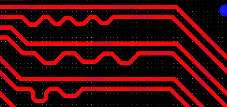
1. Use Short and Direct Signal Paths
In high-speed designs, longer traces become transmission lines. This causes delays and possible signal degradation. The longer the path, the more distortion your signal might encounter. That’s why you should keep all critical nets—like clocks, differential pairs, and high-speed data lines—as short and direct as possible.
For example, a 2-inch trace might seem negligible, but at 5Gbps speeds, even a small delay could impact timing budgets. The best routing practice is to go from point A to point B without meandering.
2. Maintain Controlled Impedance
High-speed signals don’t just travel—they reflect if the impedance isn’t consistent. This is where controlled impedance routing comes in. You need to maintain a specific impedance value (typically 50Ω for single-ended or 100Ω for differential signals).
To achieve this:
Choose the correct trace width based on the PCB stackup.
Keep dielectric thickness uniform.
Avoid inconsistent copper weights.
EBest Circuit (Best Technology) helps you calculate and verify impedance before production using simulation tools and TDR measurements.
3. Avoid 90-Degree Trace Bends
Sharp bends look neat, but at high frequencies, they act like mini antennas. A 90-degree corner changes the trace width at the bend, creating impedance discontinuity and increasing EMI.
Instead of sharp corners, route traces using:
Two 45-degree angles
Or a smooth arc
This method maintains uniform impedance, reduces reflections, and looks cleaner from a manufacturing standpoint.
4. Implement Solid and Continuous Ground Planes
Every signal needs a return path, and that path usually travels directly under the trace on the ground plane. If that plane is broken or has cutouts, the return path becomes longer and induces unwanted noise.
To fix this:
Place a solid, unbroken ground plane beneath high-speed layers.
Avoid crossing plane splits with high-speed signals.
Minimize layer transitions that force return paths to detour.
EBest Circuit (Best Technology) uses dedicated ground planes and simulation validation to ensure return paths are uninterrupted.
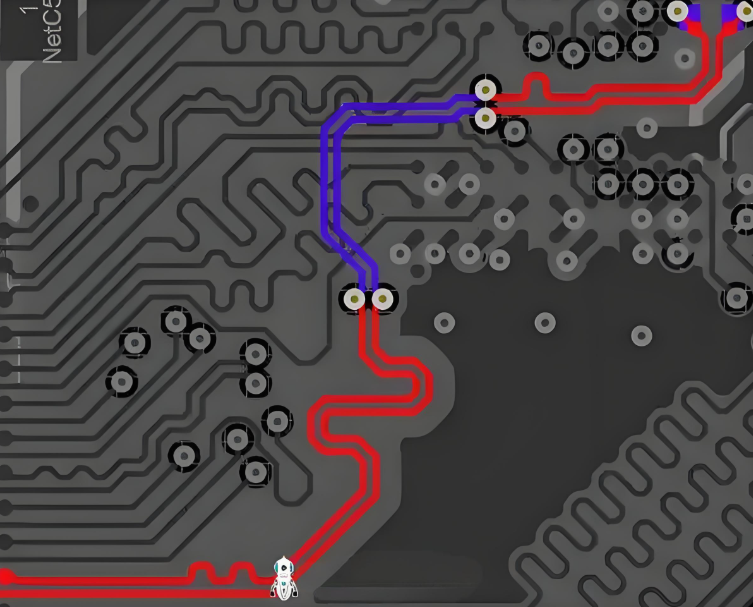
5. Match Lengths of Differential Pairs
Differential pairs, such as USB, HDMI, or LVDS lines, must be length-matched to prevent signal skew. If one trace is longer than the other, the timing mismatch can cause errors.
Some tips:
Match lengths to within a few mils.
Maintain consistent spacing (edge-to-edge).
Route them together, avoiding different layers unless absolutely needed.
At EBest Circuit (Best Technology), we support tight differential pair matching down to ±5 mil during production.
6. Minimize the Use of Vias
Every via adds capacitance and inductance, which degrades signal quality. High-speed signals don’t like jumping between layers unless absolutely necessary.
If you must use vias:
Keep them short and consistent.
Avoid unnecessary layer transitions.
Use via stitching to maintain continuous return paths.
Our engineering team optimizes via placement and offers blind and buried vias for complex HDI boards to reduce signal loss.
7. Use Proper Termination Techniques
Termination prevents reflections and stabilizes high-speed signals. Whether it’s series, parallel, or AC termination, it depends on your driver and load setup.
For instance:
Series termination works well for point-to-point connections.
Parallel termination helps in multi-drop setups.
Improper termination can cause overshoot, ringing, or logic errors. We assist customers in selecting proper termination resistors during DFM review.
8. Isolate Analog and Digital Grounds
Mixing analog and digital signals is risky. Digital circuits generate switching noise that can interfere with sensitive analog components.
Good layout practices include:
Keeping analog and digital circuits physically separated.
Avoiding crossover between analog and digital return paths.
Using ground islands connected at a single point if necessary.
Our layout reviews always evaluate signal isolation to avoid interference in mixed-signal boards.
9. Route Differential Pairs Together
Differential pairs must be routed together, in parallel, and on the same layer. If one signal strays away or loops, it creates an imbalance, which defeats the benefit of differential signaling.
Also:
Avoid routing them across split planes.
Keep them tightly coupled (consistent spacing).
Avoid fan-out unless necessary at termination points.
Our advanced PCB manufacturing equipment keeps tight trace spacing and alignment even on high-density interconnects (HDI).
10. Observe Return Current Paths
High-speed return currents don’t follow the shortest path—they follow the path of least inductance, usually right beneath the trace.
Interrupting that path causes:
Ground loops
Crosstalk
Increased EMI
To prevent this:
Avoid crossing plane splits with signal traces.
Use stitching vias to keep the return path near.
Place decoupling capacitors close to where the signal changes layer.
We validate return paths during layout verification using signal integrity tools.
11. Use Stitching Capacitors and Ground Vias
To suppress high-frequency noise and EMI:
Use stitching capacitors between power and ground.
Place ground vias near signal transitions and connectors.
These components act like firewalls, keeping noise from traveling across the board.
We help customers determine the best placement for decoupling caps and ground stitching to maintain signal purity.
Why Trust EBest Circuit (Best Technology) for Your High-Speed PCB Projects?
At EBest Circuit (Best Technology), we specialize in advanced PCB manufacturing and assembly solutions, supporting industries like automotive, aerospace, medical, and telecom. With ISO-certifications, we bring rigorous quality control to every project.
Since its establishment in 2006 as a printed circuit board manufacturer, EBest Circuit (Best Technology) has focused on high-quality, low to medium-volume PCB fabrication, PCB assembly and electronics manufacturing. Our products and services include 1-40 layers printed circuit boards, thru-hole assembly, SMT assembly including BGA assembly, components sourcing, turnkey box build and electronic product development. Whether you need quick-turn prototypes or volume production with controlled impedance, we’re your reliable partner in high-speed design.
High-speed PCB design is more than just routing—it’s about understanding physics, signal behavior, and layout strategy. At EBest Circuit (Best Technology), we not only manufacture your boards, but also optimize them for real-world performance.
Whether you need HDI PCBs, controlled impedance, differential pair routing, or quick prototypes, our team is ready to help.
👉 Let’s turn your next design into a high-speed success. Contact us now to get a quote or design consultation!
Frequently Asked Questions (FAQs)
1. What is considered a high-speed signal in PCB design?
Any signal with a rise/fall time below 1ns or operating above 100MHz is considered high-speed, as it starts behaving like a transmission line.
2. Can I use auto-routing for high-speed signals?
Auto-routers are not recommended for high-speed nets. Manual routing provides better control over trace length, impedance, and matching.
3. What is skew in differential pairs?
Skew refers to the time delay between the two signals in a differential pair. Skew can cause data errors and must be minimized.
4. How do I calculate trace impedance?
Trace impedance depends on trace width, thickness, dielectric height, and PCB material. Use online calculators or simulation tools like Polar or Altium.
5. Can I run high-speed signals on outer layers?
It’s better to route high-speed signals on internal layers between solid ground planes to reduce EMI and maintain impedance.
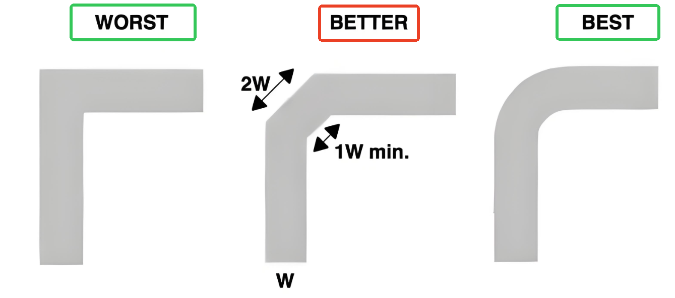
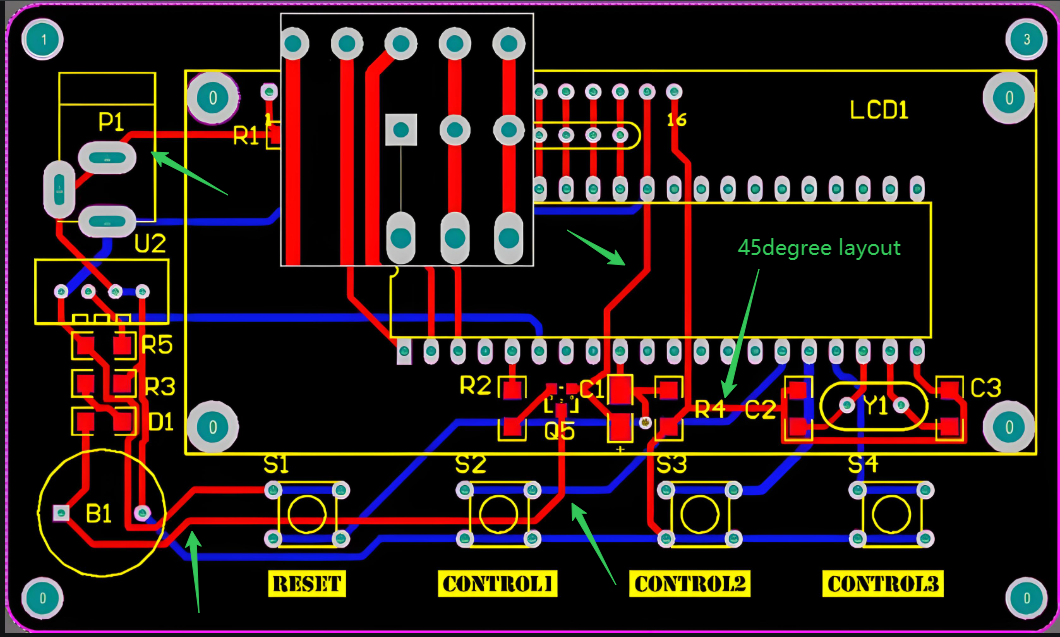
In PCB layout design, routing angles have a direct impact on signal integrity, manufacturing quality, and overall board performance. The two most common routing angles—45-degree and 90-degree—have long been debated among engineers and designers. While both have their uses, the choice between them depends on electrical performance, fabrication processes, and design goals.
This blog explores the differences between 45-degree and 90-degree routing angles. We’ll break down how each angle affects your board’s reliability, signal flow, and manufacturability. You’ll also get practical insights into when and why to choose one over the other.
Why Routing Angles Matter in PCB Design?
Routing angles may seem like a minor detail, but they carry more weight than you might expect. When copper traces change direction sharply, it impacts how current flows through the circuit. This is especially critical for high-speed and high-frequency designs. Uneven trace transitions can cause reflections, impedance discontinuity, and even signal degradation.
Aside from performance, routing angles influence how easy it is to manufacture, etch, and inspect the board. Smooth routing not only helps the signals but also improves the final product’s consistency and durability.
What Is a 90-Degree Routing Angle?
A 90-degree angle in PCB routing refers to a sharp right-angle corner where a trace takes a turn. It is often called a right-angle bend and used mostly in older or simpler PCB layouts.
Characteristics:
Easy to draw and route.
Common in low-frequency, analog, or single-layer PCBs.
Produces a clear, angular look on CAD tools.
Despite its simplicity, the 90-degree bend has downsides when it comes to electrical performance and manufacturing precision, which we’ll explore in detail later.
What Is a 45-Degree Routing Angle?
A 45-degree angle is a more gradual, beveled bend in PCB traces. Instead of a sharp corner, the trace changes direction at an angle, forming a smoother path. Some layouts even use two 45-degree bends to make a soft curve.
Characteristics:
Smoother current flow.
Reduced signal reflection.
Preferred for high-speed and high-frequency circuits.
Many modern CAD tools default to 45-degree routing due to its positive effect on signal integrity and trace etching quality.
Main Differences Between 45-Degree and 90-Degree Angles
Feature
45-Degree Angle
90-Degree Angle
Signal Integrity
Better, due to smooth transitions
Worse, due to corner reflections
EMI/EMC
Lower emissions
Higher emissions
Manufacturing
Easier to etch; fewer defects
Etch traps can form at corners
Trace Length
Slightly longer
Shorter, more direct
CAD Complexity
Slightly harder to route manually
Very easy to route
Aesthetic & Professionalism
Industry standard for high-speed
Looks dated in modern designs
Why 90-Degree Angles Can Be a Problem?
1. Impedance Discontinuity
Sharp corners create impedance mismatches that disrupt uniform signal travel. This is especially noticeable in controlled impedance traces, where precision is key. Signal reflection at a 90-degree turn can distort waveforms and cause errors in communication lines.
2. Electromagnetic Interference (EMI)
A sharp angle acts like a small antenna. This increases electromagnetic emissions, which may lead to your product failing EMI compliance tests. It also raises the risk of cross-talk in dense layouts.
3. Etching Defects
During fabrication, etching around a sharp 90-degree corner can cause acid traps, where chemical etchants get stuck and over-etch the copper. This can weaken the trace or cause open circuits.
4. Signal Reflection
Right-angle bends can cause signal reflection and ringing, particularly at high frequencies. This distorts the signal waveform and affects timing, which is critical in fast digital or RF systems.
Why 45-Degree Routing Is Widely Used?
The use of 45-degree routing in PCB design has become a standard practice in the industry. While older layouts sometimes featured sharp 90-degree angles for simplicity, most modern PCB designs now adopt 45-degree bends. Below are the key factors that explain why 45-degree routing is widely used.
1. Smoother Signal Transitions
In high-speed PCB designs, signal integrity is everything. Signals travel along copper traces like waves, and any abrupt direction change can reflect or distort the waveform. A 90-degree corner creates a sudden path change, which introduces a small but sharp discontinuity.
2. Lower Electromagnetic Interference (EMI)
Electromagnetic interference (EMI) is a growing concern in today’s electronics, especially in wireless and communication systems. Sharp trace corners such as 90-degree bends tend to behave like antennas. They concentrate electric fields and can emit higher levels of radiation, contributing to EMI. Designs that follow 45-degree routing are more likely to pass EMI compliance tests and meet international standards for electromagnetic compatibility.
3. Improved Manufacturability
From a manufacturing point of view, sharp corners can introduce several problems. During the etching process, chemical etchants used to remove unwanted copper may get trapped in 90-degree corners. These are known as acid traps. They can lead to over-etching, where too much copper is removed, or even undercutting, which weakens the trace at the bend.
4. Better Heat Distribution
Although routing angles don’t directly affect thermal conductivity, trace shapes can influence heat flow, especially in power boards. Smooth traces, like those formed with 45-degree bends, allow more even heat distribution along the path. Sharp corners may act as stress points where heat can build up, potentially weakening the copper over time.
5. Supports High-Speed and RF Design Standards
High-speed digital and RF designs demand strict control over trace geometry, impedance, and layout structure. In such designs, even minor trace irregularities can lead to signal degradation, noise coupling, or timing issues. Most high-speed PCB design guidelines—such as those for DDR memory, USB 3.0, HDMI, or RF transceivers—explicitly discourage the use of 90-degree angles.
How to Avoid 90-Degree Angles in PCB Design?
Most PCB layout software supports angle snapping, which makes it easy to design 45-degree routes. Here are a few tips:
Use 45-degree snap mode in your routing tool.
Use arc routing for smoother transitions in sensitive areas.
Double-bend technique: Instead of a single 90-degree, use two 45-degree bends to redirect the trace.
Check your DRC (Design Rule Check) for right-angle warnings if available.
Many RF and microwave design rules prohibit 90-degree bends.
Professional board reviewers often flag right angles as poor practice.
Following these standards doesn’t just improve performance—it also gives clients and manufacturers confidence in your designs.
Common Myths About Routing Angles
Myth 1: 90-Degree Bends Always Break the Signal
Not always. If you’re working with low-speed signals or power lines, the impact is negligible. The problem grows with frequency, edge rate, and sensitive signals.
Myth 2: 45-Degree Routing Takes More Space
It may take a tiny bit more space, but not enough to justify poor signal integrity. Most modern designs can accommodate 45-degree bends with minor effort.
Myth 3: 90-Degree Angles Are Cheaper to Fabricate
Not true. They can actually increase manufacturing costs due to over-etch risks or inspection failures.
Why Choose EBest Circuit (Best Technology) for PCB Design and Manufacturing?
At EBest Circuit (Best Technology), we go beyond just making PCBs. We help you design better boards from the start. Whether you’re routing high-speed digital signals or managing dense analog layouts, our engineering team follows best practices—including angle rules—to improve your product’s performance.
We are certified under ISO9001, ISO13485, IATF16949, and AS9100D, with an MES system that ensures traceability and quality control. We specialize in both standard and complex PCB manufacturing, including HDI, RF, and metal-core designs.
Contact Us Today
If you need help with routing strategy or want high-quality PCB production, our team is ready. From prototype to volume production, we can support your needs with fast delivery, quality control, and engineering guidance.
📩 Reach out now to get your quote and talk to our experts.
FAQs
1. Do 90-degree angles always cause EMI issues?
Not always. At low frequencies, the impact is minimal. But in high-speed or RF designs, they can be problematic.
2. Is 45-degree routing mandatory for all traces?
It’s not mandatory, but it’s highly recommended for signal traces, especially in complex or fast designs.
3. Can I use rounded corners instead of 45-degree angles?
Yes. Rounded corners are even better for very high-speed signals but may increase layout complexity.
4. Are 90-degree bends allowed in power planes?
Yes. Since power planes don’t carry high-speed signals, 90-degree turns are generally safe there.
5. How can I check for right angles in my layout?
Use your PCB tool’s DRC (Design Rule Check) to scan for sharp angles or manual review if needed.
Electron devices and circuits are the foundation of modern electronics. From smartphones and computers to medical scanners and satellite systems, these components quietly manage the flow of electricity behind the scenes. This blog explores how they work, what types exist, and how they power the electronic world around us.
What Are Electron Devices?
Electron devices are components that either control, modify, or amplify electrical signals. These devices rely on the movement of electrons to function and are used in countless applications, from simple toys to complex industrial machinery. Their job is to manage electrical energy in ways that produce useful output—such as turning on lights, processing data, or amplifying sound.
At their core, electron devices convert electrical energy into other forms or modify electrical signals to perform a specific function. Without them, modern electronic systems wouldn’t be possible.
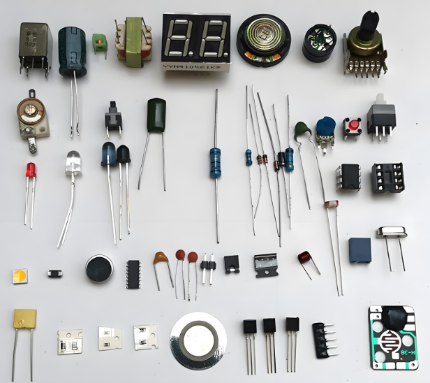
Types of Electronic Devices
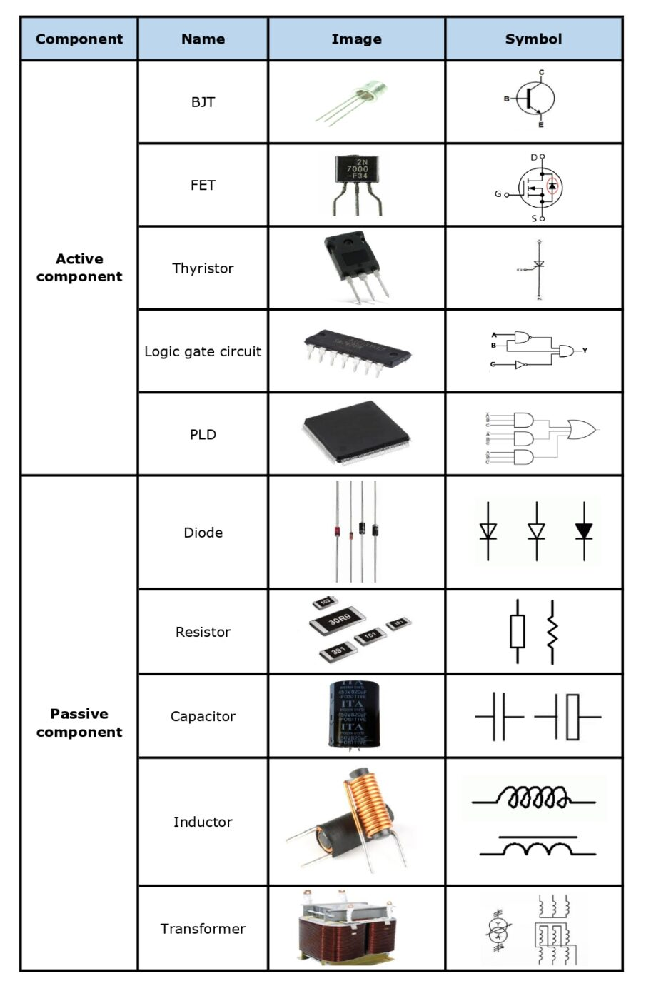
Each electronic component has specific properties that determine how it behaves in a circuit. The choice of components depends on the designer’s goal and the function the circuit is meant to perform. The image below highlights common electronic components used across various types of circuits. To better understand their roles, components are generally classified into two categories: Active Components and Passive Components.
1. Active Devices
Active devices can control current flow and even amplify weak electrical signals. These devices require an external power source to operate. Some common active devices include:
Transistors: Used in amplifiers and switches.
Diodes: Let current flow in one direction.
Integrated Circuits (ICs): Tiny packages that contain complex electronic functions.
Active devices are central to any system that processes signals, computes information, or boosts communication signals.
2. Passive Devices
Passive devices do not generate energy. Instead, they store, dissipate, or transfer it. Common examples include:
Resistors: Limit the flow of current.
Capacitors: Store and release electrical energy.
Inductors: Resist sudden changes in current.
These components support the work of active devices and help shape how signals behave in a circuit.
What Are the 5 Basic Electronic Devices?
The five basic devices you’ll find in nearly every circuit are:
Resistor
Resistors manage the current flowing through different parts of a circuit. They help in dividing voltage, controlling signal levels, and protecting components from excessive current.
Capacitor
Capacitors store electrical charge temporarily. They’re used in filtering noise, smoothing power supply outputs, and creating time delays.
Inductor
Inductors store energy in a magnetic field when current flows through them. They’re commonly used in filters, power supplies, and transformers.
Diode
Diodes allow current to flow in only one direction. They are essential in power rectification, signal demodulation, and voltage regulation.
Transistor
Transistors act as switches or amplifiers. They control the flow of current and are fundamental to logic circuits and digital electronics.
How Do Electronic Devices Work?
Each electronic device has a specific function based on its physical and electrical characteristics:
Resistors slow down current.
Capacitors store energy in an electric field.
Inductors build magnetic fields.
Diodes control direction.
Transistors regulate and amplify signals.
Together, these devices shape how electricity behaves inside a circuit. When connected in specific arrangements, they form circuits capable of performing tasks like amplifying a sound, storing digital information, or controlling a motor.
What Are Electronic Circuits?
An electronic circuit is a system of connected components that guide electrical currents to perform a specific job. These circuits can be as simple as a battery lighting an LED or as complex as the logic boards inside a computer.
Circuits make electronic devices work by controlling where and how electricity flows. Each component in the circuit has a role—some store energy, others shape signals, and some respond to external inputs like light or sound.
Types of Electronic Circuits
Electronic circuits come in a few major types, depending on how they handle signals:
Analog Circuits
Analog circuits work with continuous signals. They are used in audio systems, radio receivers, and temperature sensors. They process real-world inputs like sound or light.
Digital Circuits
Digital circuits work with binary signals (0s and 1s). They form the backbone of computers, smartphones, and digital watches. Logic gates and microcontrollers are key components.
Mixed-Signal Circuits
These combine analog and digital elements. Examples include digital audio converters, embedded controllers, and power management circuits.
Key Components in Electronics Circuits
A functioning circuit depends on a combination of components, each with a distinct role:
Power Supply: Provides the necessary voltage and current.
Resistors: Manage current flow and protect sensitive parts.
Capacitors & Inductors: Shape or filter signals and manage timing.
Diodes & Transistors: Control signal direction, switching, and amplification.
Integrated Circuits (ICs): Combine multiple components in one small package for complex functions.
Switches, Connectors & PCBs: Physically support and route current throughout the system.
All these parts are arranged on a printed circuit board (PCB), which provides the mechanical structure and electrical connections.
How to Design an Electronic Circuit?
Designing a circuit starts with a clear goal. Once the purpose is defined, follow these steps:
Outline Your Requirements: What do you want the circuit to do?
Create a Schematic: Use circuit design software to build the layout using symbols for each component.
Select Components: Choose values for resistors, capacitors, etc., based on your requirements.
Simulate the Circuit: Check how it behaves using tools like LTspice or Proteus.
Build a Prototype: Use a breadboard or PCB to assemble and test your design.
Test & Debug: Measure voltages and currents to confirm it works as expected.
Final Layout: Once tested, you can design a PCB for the final version.
Even simple circuits need careful planning, as incorrect wiring or value choices can lead to failure or inefficiency.
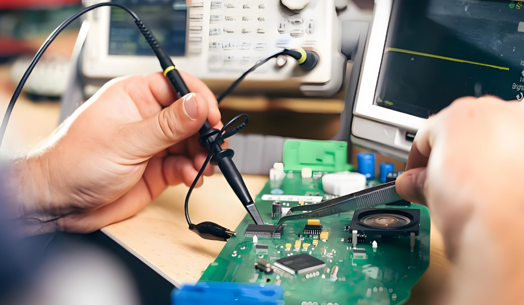
Common Measurement Devices for Electronic Circuits
To check and troubleshoot circuits, engineers use various tools:
Multimeter: Measures voltage, current, and resistance. Essential for almost any testing.
Oscilloscope: Displays how signals change over time—helpful for analyzing waveforms.
LCR Meter: Measures inductance (L), capacitance (C), and resistance (R).
Logic Analyzer: Helps in debugging digital signals and timing issues.
These devices ensure that the circuit performs properly under different conditions.
Applications of Electron Devices and Circuits
Electron devices and circuits power virtually all technology we use today. Here are a few major application areas:
Consumer Electronics: Televisions, phones, game consoles, and home appliances all rely on sophisticated circuits.
Automotive Systems: Used in engine control units (ECUs), ABS brakes, GPS modules, and more.
Medical Devices: Circuits manage everything from heart monitors to imaging systems.
Telecommunications: Signal boosters, routers, and network devices depend on electronic components.
Industrial Equipment: Used in automation, robotics, and machine control systems.
Defense & Aerospace: Critical in radar systems, flight control computers, and satellite communications.
No matter the industry, the role of electron devices and circuits is critical in innovation, performance, and safety. Whether you’re a student, hobbyist, or professional, grasping how circuits function and how devices interact is essential to designing or repairing electronic equipment.
For those looking to build reliable circuit boards or need help bringing their electronic designs to life, partnering with an expert manufacturer is key.
Why Choose EBest Circuit (Best Technology) for Electronic Circuit Projects?
EBest Circuit (Best Technology) is a trusted PCB manufacturer specializing in both prototype and volume production. With ISO-certifications, our team ensures your circuits meet international standards. Whether you need rigid PCBs, flexible circuits, or mixed-signal board assemblies, we help turn your ideas into high-quality products—on time and within budget. By choosing EBest Circuit (Best Technology), you can enjoy:
1. Fast Turnaround from Prototype to Mass Production
We help you move quickly from design to final product. Whether it’s a first-run prototype or a full production batch, we adapt to your schedule and keep your project on track.
2. Hands-On Engineering Support
Our experienced engineers work with you on component selection, stack-up optimization, and layout suggestions—helping you avoid design flaws before production begins.
3. High Customization, No Fear of Complexity
Need a non-standard stack-up, hybrid materials, or bendable structures? We handle complex builds with confidence and tailor every detail to match your design requirements.
4. Clear Quotes and On-Time Delivery
Our pricing is transparent, and our timelines are realistic. Dedicated project coordinators provide regular updates, so you’re never left guessing.
5. Quality is a Daily Practice, Not Just a Promise
We don’t just inspect a few boards—we test every unit. From flying probe tests to X-ray and AOI, our quality process ensures every board performs reliably.
FAQs
1. What’s the difference between an electronic and electrical device?
Electronic devices use the flow of electrons to process signals, while electrical devices typically handle power distribution and energy conversion.
2. Can I build electronic circuits without a PCB?
Yes, prototypes are often built on breadboards or perfboards, but PCBs are used for stability and durability in final products.
3. What software is best for circuit design?
Popular tools include KiCad, Eagle, Altium Designer, and Proteus for simulation and layout.
4. What is the most common cause of circuit failure?
Overheating, poor soldering, incorrect component values, or voltage surges are common failure causes.
5. How do I start learning electronics as a beginner?
Start with basic components, build simple circuits using breadboards, and gradually move to microcontroller projects using kits like Arduino or Raspberry Pi.
Printed circuit board switches (PCB switches) are an integral component in electronic devices that allow current to flow or be interrupted in a circuit. Among them, PCB dome switches offer crisp tactile feedback, high reliability, and easy integration, making them ideal for everything from consumer devices to industrial panels.
What is a PCB switch?
PCB switch is a control device mounted on a printed circuit board. It allows users to interact with electronics through simple actions. Turning a device on, changing a setting, or starting a function often happens with a PCB switch.
They come in various forms. Some are tactile. Others are soft-touch. Some are designed for heavy use. All types share a goal: precise, responsive user input.
Small in size, PCB switches deliver big performance. Their design ensures low-profile, efficient operation across many devices.
How does a printed circuit board switches work?
PCB switches complete circuits when pressed. Two contacts inside the switch touch, allowing current to flow. This flow sends a signal to the device’s processor. Once released, the contacts separate and the signal stops.
Some switches use rubber or plastic materials. Others use metal domes. No matter the type, the process is consistent. They translate physical action into digital output.
What are circuit board switch types?
There’s a wide range to explore. Some of the most common circuit board switch types include:
Tactile switches: These give a distinct click when pressed. Perfect for user interfaces.
Toggle switches: Often found in industrial settings, they flip between states.
Push button switches: Simple and efficient. Often used in consumer electronics.
Slide switches: Move side-to-side to open or close a circuit.
Rotary switches: Used for controlling devices with multiple options.
Membrane switches: Flat and sealed, ideal for wet or dusty environments.
Dome switches (including metal domes): Deliver tactile feedback and durability.
Each type serves specific purposes. Some are built for rugged use, others for sleek designs.
How do you choose PCB switch types?
Choosing the right switch isn’t just about size. It’s about function, environment, and experience.
First, consider the application. Is it for a wearable or a medical device? Does it need water resistance or high responsiveness?
Next, focus on the feel. Tactile feedback can enhance user satisfaction. For example, a solid click feels more secure than a mushy press.
Durability is key. If your product requires millions of cycles, dome switches or metal dome are top contenders.
Mounting style also matters. Surface-mount technology (SMT) is ideal for automated processes. Through-hole switches are better for heavy-duty usage.
Lastly, never ignore cost versus performance. Striking the right balance ensures both user happiness and budget control.
Where are PCB switches used?
Everywhere. They’re found in:
Smartphones and tablets
Wearable fitness trackers
Automotive dashboards
Medical monitoring equipment
Consumer appliances
Industrial controls
Gaming consoles and controllers
Smart home devices
PCB switches keep our devices functional, responsive, and enjoyable to use. Without them, even the most advanced system becomes difficult to operate.
What is a PCB dome switch?
PCB dome switch is a special kind of tactile switch. It uses a metal dome to complete a circuit. When pressed, the dome collapses and bridges the contacts underneath.
The beauty lies in its simplicity. When released, the dome returns to shape, breaking the connection. This mechanism ensures long-lasting reliability and quick response times.
Metal domes are especially favored for their sharp tactile feel. Users feel that satisfying “snap” which confirms the input was registered.
Why use metal domes for circuit board switches?
Metal domes offer a blend of sensitivity and strength. Their advantages include:
Crisp tactile feedback: Users know exactly when a button is pressed.
High durability: Many domes last over 1 million cycles.
Slim profile: Ideal for sleek, compact designs.
Fast response: Instant signal when activated.
Corrosion-resistant: Especially when made from stainless steel.
Metal domes work across different applications. Whether in medical gear or touch panels, they perform consistently. They also resist wear and temperature shifts. That’s why they are used where precision matters.
How is a metal dome switch different?
Metal domes outperform rubber and membrane layers in many areas.
Unlike membrane switches that rely on pressure-sensitive layers, metal dome switches use a physical component to create contact. This makes them more tactile, with less chance of accidental activation.
Compared to rubber domes, metal domes are more consistent. They don’t degrade as fast and hold up under heavy use.
Also, metal dome switches are cleaner. There are fewer moving parts and minimal debris generation. In critical fields like medical and aerospace, this matters.
How do metal dome switches work on PCBs?
Metal domes sit over circuit contacts. It may sit on a spacer or adhesive film or held within a dome array.
When pressed, the dome collapses. It connects the circuit beneath. Release it, and the dome returns to shape. This makes and breaks the signal.
Dome arrays make installation easier. Each dome aligns with its PCB contact. Assembly becomes fast and accurate.
These switches support mass production. SMT machines can place them quickly. You can also fine-tune dome properties—like snap force and shape.
Conclusion:
Printed circuit board switches are at the heart of modern electronic control. From standard tactile switches to high-performance metal domes, these components create that essential connection between people and machines.
Among all the options, PCB dome switches—especially metal dome switches—stand out for their tactile feel, durability, and reliability. They’re the preferred choice when performance and user experience matter most.
For more information or to request samples, contact us today at sales@bestpcbs.com
A DTP MCPCB, or Direct Thermal Path Metal Core PCB, also known sinkpad MCPCB, is a type of printed circuit board designed for high-power and high-heat applications. It helps electronics stay cool and stable, even under heavy loads. Compared to standard MCPCBs, DTP PCBs offer better thermal transfer and stronger mechanical support. Many industries, including LED, power supply, automotive, and telecom, now prefer DTP copper MCPCBs for reliable performance.
In this blog, we’ll explain what DTP means, its features, structure, design tips, manufacturing process, and how it fits into modern electronics.
What Is DTP and Its Features?
DTP stands for Direct Thermal Path. It refers to a design where heat moves directly from hot components to the metal base without many thermal barriers. This path lowers thermal resistance and keeps components cooler.
Main Features of DTP:
Direct connection between heat source and metal base
Higher heat dissipation than traditional MCPCBs
Stronger thermal conductivity through thick copper or copper convexity
Better reliability in high-power circuits
Long-lasting even under thermal cycling and vibration
This structure reduces the chance of overheating, which helps the whole system run longer and safer.
DTP Copper MCPCB Structure
A DTP copper MCPCB uses a raised copper structure (called a copper convexity or copper boss) formed directly on the metal base. This convex feature aligns under the heat source, typically a power component like a MOSFET or high-wattage LED. The DTP copper PCB layers are:
Top Layer: Copper trace for electrical routing
Dielectric Layer: High thermal conductivity insulation
Copper Convexity: Directly contacts both the component and the base
Metal Base: Usually aluminum or copper for heat spreading
Its stackup layers is:
This design bypasses traditional insulation layers and allows heat to flow directly into the metal core.
DTP MCPCB vs Traditional MCPCB
Standard MCPCBs have a thin dielectric layer between the copper trace and the metal base. This layer adds thermal resistance. In contrast, a DTP PCB reduces this resistance by forming a direct path between the component and the base metal using copper convexities.
Feature
DTP MCPCB
Traditional MCPCB
Heat Transfer
Direct (through copper convexity)
Through dielectric
Thermal Resistance
Very Low
Medium
Use Case
High-power, LED, EV, power supply
General LED, moderate power
Cost
Higher
Lower
Performance
Excellent
Good
Where Are DTP PCBs Used?
DTP MCPCBs are perfect for any application where heat is a big issue. They’re now standard in many thermal-critical products. The main applications including:
High-power LED lighting
Power supplies and inverters
Electric vehicles (EVs) and battery packs
RF and telecom base stations
Solar energy systems
Laser modules and sensors
Whenever components get hot and space is tight, DTP copper MCPCBs offer a smart solution.
Tips for MCPCB Design with DTP Structure
Designing a DTP PCB requires special attention to thermal paths, layout, and material selection.
Place heat-generating components directly over copper convexities
Use high-conductivity dielectric materials to keep thermal resistance low
Align thermal vias with component pads for effective heat flow
Choose a suitable base material: aluminum for cost, copper for performance
Ensure planarity and flatness for solid thermal contact
A carefully designed DTP MCPCB handles more power without compromising safety or reliability.
Why Is the Price of DTP MCPCB Higher Than a Normal MCPCB?
The cost of a DTP MCPCB is higher due to the complexity of its design and processing. It uses thicker copper or custom copper convexities, which are more expensive than standard copper foil. Creating a precise raised copper feature under each heat source requires extra machining steps, tight alignment, and rigorous quality checks.
Additionally, the dielectric materials used must have very high thermal conductivity and are usually more costly. The manufacturing process also involves advanced methods like X-ray alignment, CNC machining, and thermal performance testing. Despite the higher price, DTP MCPCBs offer long-term savings by improving thermal efficiency, reducing failure rates, and extending product lifespan.
How DTP MCPCBs Are Manufactured?
The manufacturing of a DTP MCPCB is more advanced than a standard MCPCB manufacturing process. It focuses on forming a raised copper boss (convexity) that provides a one-piece thermal bridge between the heat source and the metal base.
1. Base Metal Preparation
The aluminum or copper base is cleaned and pre-treated. This forms the foundation for the entire board.
2. Creating the Copper Convexity
A raised copper feature is formed on the base metal. This copper boss is placed directly beneath high-heat components. The convexity may be CNC machined or created during the copper plating process.
3. Dielectric Layer Lamination
A thin, high-thermal-conductivity dielectric is laminated around the copper convexity and onto the metal base. The copper bump remains exposed to make direct contact with the top copper circuit.
4. Copper Foil Application & Circuit Etching
Copper foil is laminated onto the surface and patterned using photolithography. The exposed part of the copper boss connects directly to a pad on the top layer.
5. Drilling & Plating (if required)
If the design includes signal vias or multi-layer connections, micro-drilling and copper plating are applied carefully to avoid damaging the copper boss.
6. Solder Mask & Surface Finish
Solder mask is printed, leaving heat transfer pads exposed. Surface finish (e.g., ENIG, HASL) is applied for soldering protection.
7. Inspection & Testing
X-ray confirms alignment of copper convexity under the pad
Thermal resistance is measured
Electrical continuity is tested
Visual and mechanical checks ensure no delamination or defects
This process requires tight process control and high-end fabrication equipment.
Benefits of Using DTP Copper MCPCB in High-Power Electronics
Superior thermal performance for high-wattage components
Longer component life due to reduced junction temperatures
Smaller form factor with higher power density
Stable performance under vibration, shock, and thermal cycling
Improved system efficiency and lower cooling requirements
These benefits make DTP MCPCBs an excellent investment for demanding applications.
DTP PCB Material Choices
A high-quality DTP PCB relies on the right materials:
Copper Convexity: Pure copper, usually 1–4mm thick
Dielectric Layer: Ceramic-filled epoxy or other high-conductivity material
Metal Base:
Aluminum: Lightweight, good for general use
Copper: Best thermal conductivity, ideal for extreme conditions
The right combination depends on your project needs, thermal limits, and cost targets.
Why Work With a Reliable DTP MCPCB Manufacturer?
Not all PCB manufacturers can build DTP MCPCBs. You need a supplier with tight process control, CNC machining, and advanced lamination tools.
A good DTP supplier should offer:
Custom DTP MCPCB design support
In-house thermal simulation and analysis
CNC or stamping for copper convexity
X-ray and AOI for high-precision quality control
Quick prototyping and scalable volume production
About EBest Circuit (Best Technology)
At EBest Circuit (Best Technology), we are experts in DTP MCPCBs, aluminum PCBs, and thermal solution boards. We serve industries including LED, automotive, telecom, and medical electronics. We also use MES systems to provide full traceability of materials and processes. Our team can support you from design to mass production with reliable engineering and fast service.
Call To Action
If you’re working on a demanding project, contact EBest Circuit (Best Technology) to learn how a custom DTP copper MCPCB can power your next innovation.