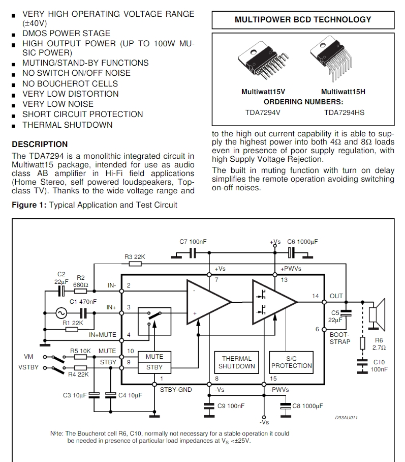
What is the full form of MCPCB
mcpcb full form is metal core printed circuit board
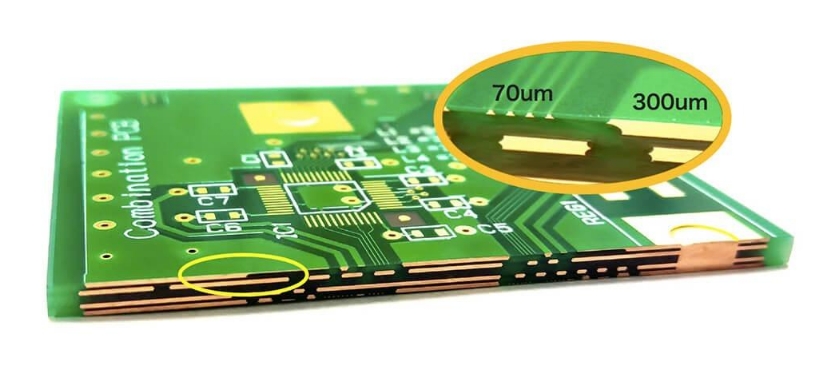
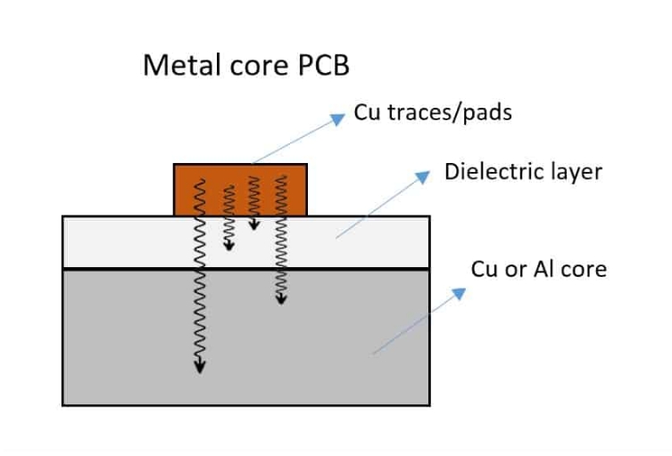
Attach the original printed circuit board to another metal with better heat conduction effect to improve the heat dissipation at the circuit board level. Metal-based PCBs usually consist of three layers: circuit layer (copper foil layer), thermal conductive insulation layer and metal base layer.
What is MCPCB
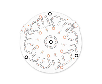
Metal Core PCB is a printed circuit board whose substrate uses metal material as a support layer or heat dissipation layer, usually an aluminum substrate or a copper substrate. It has excellent electrical conductivity and thermal conductivity.
Metal Core PCB is usually composed of a metal substrate, an adhesive and copper foil. It is characterized by high reliability, good heat dissipation, and is suitable for high-speed transmission and high-frequency circuits.
What is MCPCB
What is mcpcb led
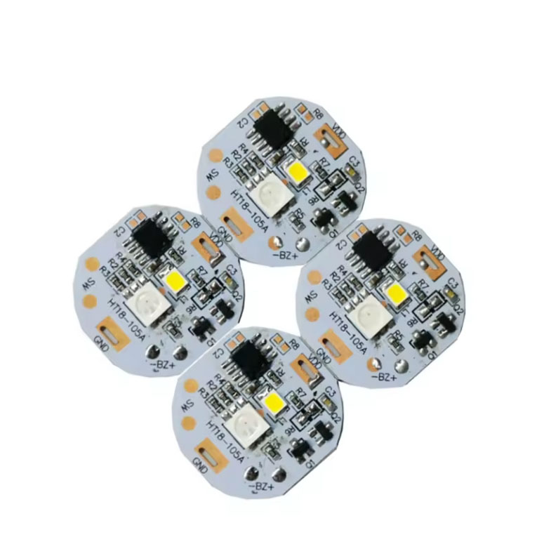
Metal-based LED lamps are LED lighting fixtures that use metal-based circuit boards (MCPCBs) as light source boards. This type of circuit board, called aluminum-based copper-clad circuit boards (ALPCBs), has excellent thermal conductivity and high cost-effectiveness, and has rapidly become the first choice for light source boards of LED lighting fixtures since 2007. The basic structure of a metal-based circuit board includes a conductive layer (copper foil layer), an insulating heat dissipation layer, and a metal base layer (mostly aluminum or copper), which together provide good electrical insulation and heat dissipation.
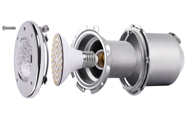
In LED lamps, it can conduct heat quickly, which is very effective in dealing with the problem of high heat generation of LEDs. Aluminum substrates also support surface mount technology (SMT), which effectively handles heat diffusion in circuit design solutions, ensuring that LED lamps have better performance and longer service life
What is the thermal conductivity of Mcpcb?
The thermal conductivity of MCPCB ranges from 1.0-4W/mK, while high-performance MCPCB can reach 230W/mK.
The thermal conductivity of MCPCB depends on its design and the materials used. Generally speaking, the thermal conductivity of MCPCB is between 1.0-4W/mK, which can already meet the heat dissipation needs of most electronic devices. However, for applications that require higher thermal conductivity, MCPCBs with thermal conductivity as high as 230W/mK have appeared on the market. This high-performance MCPCB uses special materials and designs to provide better heat dissipation.
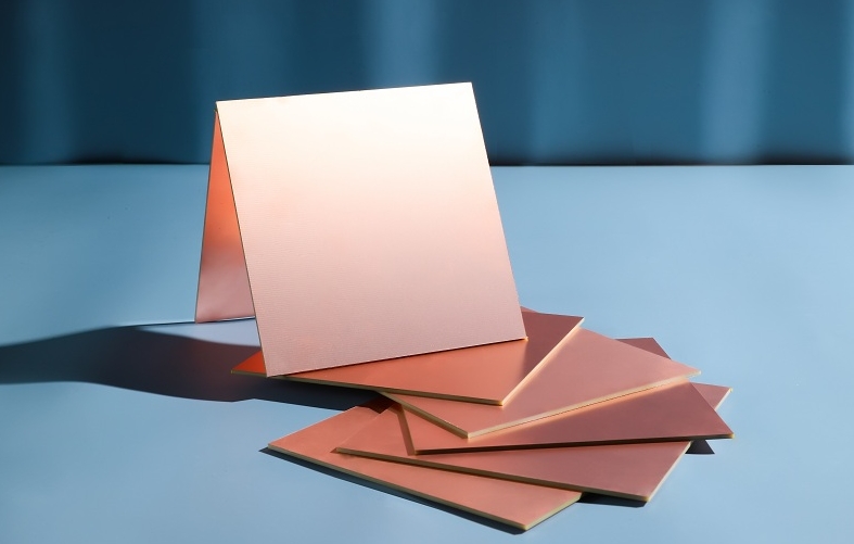
MCPCB material
- Aluminum substrate: Aluminum substrate is a metal-based copper-clad plate with good thermal conductivity and electrical insulation properties. It is usually composed of an aluminum alloy base layer and an insulating dielectric layer, and is suitable for electronic devices that require efficient heat dissipation, such as LED lighting and power supplies. Aluminum substrates can not only effectively conduct heat from the circuit board to the heat sink, but also have good mechanical strength and electromagnetic shielding effects.
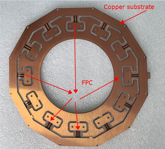
- Copper substrate: Copper substrates are known for their excellent electrical conductivity and can provide low-resistance paths, which helps improve circuit performance. Copper’s thermal expansion coefficient is similar to that of many semiconductor materials, which helps reduce thermal stress and increase component reliability.
- Tungsten substrate: Tungsten substrate has good high-temperature stability and is suitable for electronic devices in high-temperature environments. Tungsten has a low thermal expansion coefficient, which helps maintain the dimensional stability of components at different temperatures, and is suitable for high-performance electronic devices that require compact designs.
- Nickel substrate: Nickel substrate has good magnetic properties and is suitable for the application of magnetic components. Nickel substrates exhibit excellent corrosion resistance and mechanical strength under certain environments, and are suitable for electronic devices in some special environments.
- Stainless steel substrate: Stainless steel substrate is well-known for its excellent corrosion resistance and is suitable for electronic devices in some special environments. The durability and stability of stainless steel substrate make it an ideal choice for some harsh environments.
Advantages of MCPCB
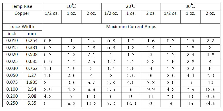
- High thermal conductivity: The thermal conductivity of metal substrate PCB is much better than that of traditional plastic substrates such as FR4. It can effectively conduct the heat generated by components, reduce the operating temperature of components, and improve the reliability and life of circuit boards.
- Good thermal stability: Metal substrate PCB can maintain good dimensional stability and electrical performance in high temperature environments, and is suitable for high temperature working environments.
- High strength and rigidity: Metal substrate PCB has high mechanical strength and rigidity, is not easy to deform and break, and can withstand large external forces and vibrations.
- Excellent electrical insulation performance: Through the special insulation layer design, good electrical insulation performance is guaranteed to avoid electrical short circuits between components.
- Low impedance: The conductive layer of metal substrate PCB is made of metal material, which has low impedance, which is conducive to signal transmission and processing.
- Good processability: Metal substrate PCB can be processed by conventional mechanical processing methods such as drilling and cutting, which is convenient for the production of circuit boards with complex shapes and sizes.
- Widely used: Aluminum substrates are widely used in audio equipment, computers, automobiles, lamps and lighting. Copper substrates are suitable for high-frequency circuits and areas with large changes in high and low temperatures.
Application of MCPCB
- Automotive electronics: The stability and reliability of metal-based PCBs make them an ideal choice in the automotive electronics field, ensuring the stable operation of automotive electronic systems.
- Medical devices: In medical devices, the high reliability and good electromagnetic compatibility of metal-based PCBs are essential to ensure the accuracy and safety of medical equipment.
- Industrial automation: Industrial automation equipment has high requirements for reliability and performance. The mechanical strength and high thermal conductivity of metal-based PCBs make them the preferred choice in the field of industrial automation.
- Communication base stations and radar systems: Communication base stations and radar systems need to process a large amount of data transmission and high-frequency signals. The excellent electrical properties and high-frequency characteristics of metal-based PCBs meet the needs of these applications.
- Antennas and filters: In the field of wireless communications, the electromagnetic shielding performance and stability of metal-based PCBs are essential to improving communication quality and reducing electromagnetic interference.
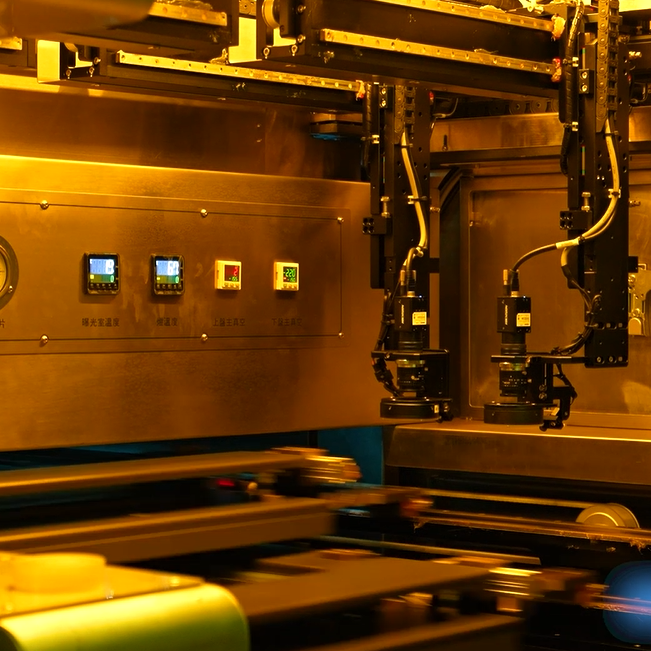
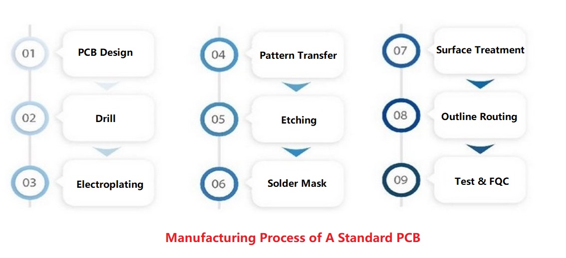
How to make MCPCB
The process flow of metal-based PCB includes inner-layer circuit production, lamination, drilling, hole metallization, outer-layer dry film, outer-layer circuit, silk-screen printing, surface processing and post-processing.
- Inner-layer circuit production: This step is mainly to produce the inner-layer circuit of the PCB circuit board, including cutting, pretreatment, lamination, exposure, DE (development, etching, film removal) and other processes, the purpose is to produce the inner-layer circuit of the PCB circuit board.
- Lamination: Press the copper foil, prepreg and brown-treated inner-layer circuit board into a multi-layer board. This step is to press multiple inner-layer boards into one board.
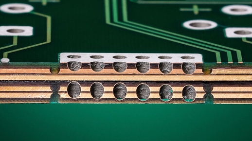
- Drilling: Use a drilling machine to drill holes of different diameters and sizes on the board according to customer requirements, so that the holes between the boards are convenient for subsequent processing of plug-ins, and can also help the board dissipate heat.
- Hole metallization: Metallizing the non-conductor part on the hole wall can make the subsequent electroplating process more convenient. This step is to plate copper in the hole so that the circuits on each layer of the board are conductive.
- Outer layer dry film: The required circuit is exposed on the dry film through graphic transfer technology, in order to facilitate the subsequent process to make the circuit.
- Outer layer circuit: The purpose is to plate the copper thickness to the thickness required by the customer and complete the circuit shape required by the customer.
- Silk screen printing: The protective layer of the outer layer circuit is used to ensure the insulation, protective plate, and solder mask of the PCB.
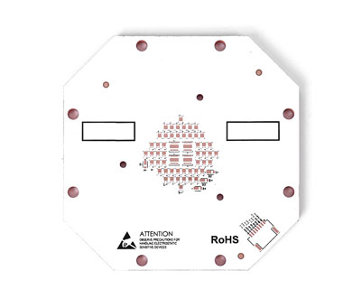
- Surface processing: Complete the processing according to the customer’s requirements, and test it to ensure the final quality audit. Both THT and SMT parts are installed on the PCB using machinery and equipment.
- Post-processing: Complete the processing according to the customer’s requirements, and test it to ensure the final quality audit.
Metal PCB Manufacturers
Welcome to our website! With over 18 years of experience in designing and manufacturing MCPCBs, we take pride in being your one-stop supplier. Our original factory spans 30,000㎡, and with a team of 229+ staff and advanced equipment, we achieve a daily peak production of up to 100k pieces.
As a trusted supplier, we hold certifications including UL, ISO13485, ISO9001, IATF16949 and SGS, enabling us to meet the high standards of clients across Europe, America, Israel, India, and so on. Our success is built on core values such as honesty, integrity, teamwork, appreciation, self-confidence, pragmatism, continuous learning, self-discipline, and fostering win-win cooperation. Experience reliability, efficiency, and quality with us. Explore our services and let us help you fulfill your MCPCB needs.
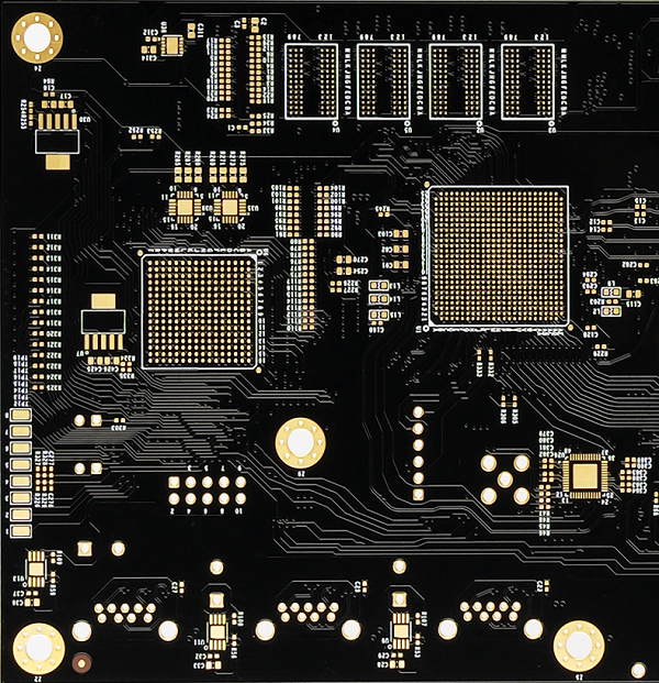
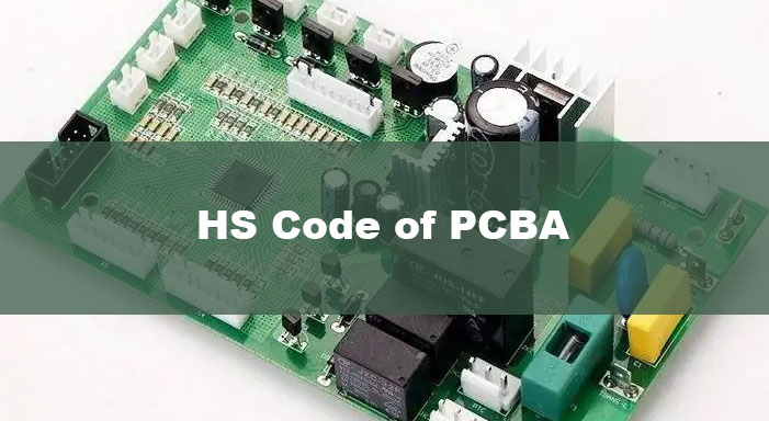
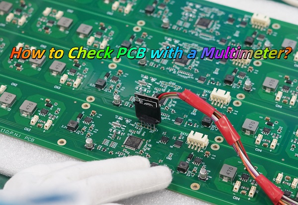
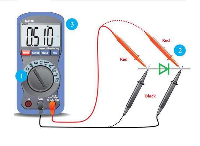
Printed circuit board assembly metal core
The preparation processes of metal matrix composite materials include contact reaction method (CR method), mixed salt reaction method (LSM method), hot pressing preparation process, stirring casting method, semi-solid composite casting method, impregnation solidification method (MI technology) and centrifugal casting method.
- Contact reaction method (CR method) is to mix the matrix element or alloy powder and the strengthening element or alloy powder in a certain proportion, cold press into a prefabricated block with a certain density, and then immerse it in an alloy melt at a certain temperature. After the reaction, a fine strengthening phase is generated in the alloy melt, and after stirring and standing, it can be cast into various castings. This method has been used to prepare a variety of metal matrix composite materials, such as Al-based, Mg-based, Cu-based, Ti-based, Fe-based, Ni-based composite materials, showing excellent mechanical properties.
- The mixed salt reaction method (LSM method) is to mix salts containing Ti and B, such as KBF4 and K2TiF6, and add them to high-temperature metal melt. The Ti and B in the salt are reduced by the metal under high temperature and react in the melt to form a reinforcing phase. After slag removal, it can be cast to obtain a reinforced metal matrix composite material.
- The hot pressing preparation process is a solid phase composite process for preparing metal matrix composite materials by diffusion bonding continuous fibers and matrix alloys at a certain heating temperature and pressure.
- The stirring casting method is to add ceramic particles to the molten metal, and after uniform stirring, pour it into the mold to obtain products or secondary processing blanks. This method is easy to achieve mass production and has low cost, but the main disadvantage is that the combination of matrix metal and reinforcing particles is limited.
- The semi-solid composite casting method is developed from the semi-solid casting method. Through strong stirring, the dendrite network skeleton is broken and the dispersed granular structure is retained, which improves wettability and promotes interface bonding.
- The impregnation solidification method (MI technology) is a method of impregnating a pre-prepared reinforcement phase formed body with a high porosity into a molten matrix metal, allowing the matrix metal to penetrate the preform and then solidify it to prepare a composite material.
- The centrifugal casting method is widely used in the casting of hollow parts. It forms a bimetallic layered composite material through a two-step casting method. This method is simple and has the advantages of low cost and high density of the casting, but the interface quality is not easy to control.