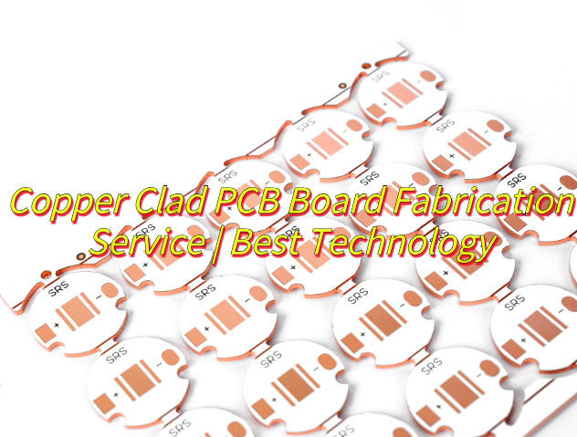
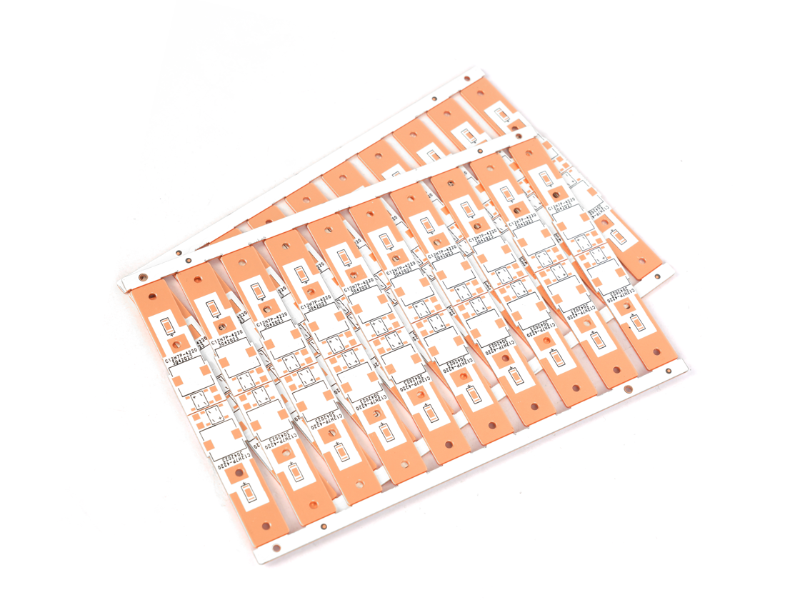
What is copper clad PCB board fabrication? Let’s discover its definition, types, applications, production process and why choose EBest Circuit (Best Technology) as copper PCB manufacturer.
Are you troubled with these problems?
High Thermal Resistance & Poor Heat Dissipation?
Unstable Processing Yield?
Small-Batch Order Barriers?
As a copper clad PCB board manufacturer, EBest Circuit (Best Technology) can provide service and solutions:
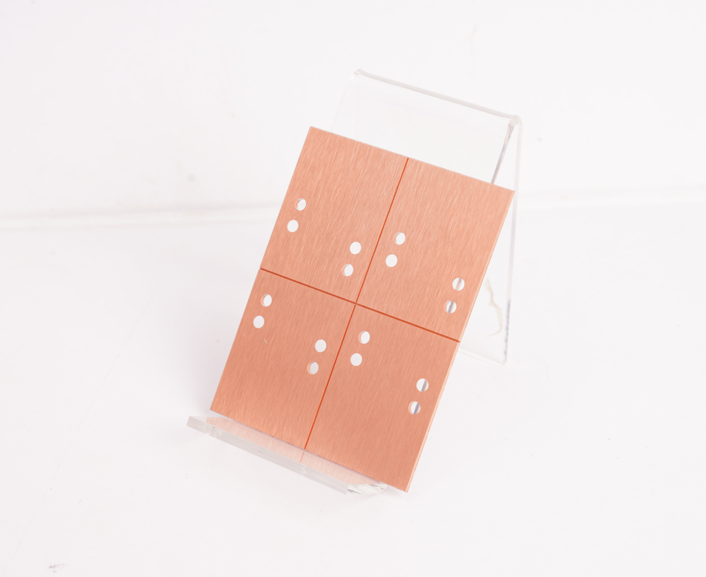
Copper Clad PCB Board Fabricationinvolves the process of securely coating an insulating substrate (such as epoxy resin) with a copper foil layer through a specific process, followed by precise etching to form conductive circuit patterns. This process leverages copper’s excellent electrical and thermal conductivity to provide a reliable physical carrier for signal transmission and heat dissipation in electronic devices.
Common Types of Copper PCB Fabrication
Single-layer Copper PCB
Single-sided copper conductive layer formed through a single etching process.
Cost-effective and simple, suitable for low-power, low-complexity applications such as household appliance control boards, LED lighting drivers, and basic sensor circuits.
Double-layer Copper PCB
Dual-sided copper layers with interlayer connectivity achieved via drilled-and-plated through-holes.
Ideal for moderately complex electronics like mobile chargers, small motor drives, and industrial controllers, enabling flexible routing and component placement.
Multilayer Copper PCB
Three or more hidden conductive layers integrated via inner-layer patterning, interlayer insulation lamination, and via/plating processes.
Designed for high-density, high-performance scenarios including 5G communication modules, automotive power systems, and medical imaging devices, supporting high-speed signal transmission, low EMI, and efficient thermal management.
Applications of Copper Clad PCB Board Fabrication
5G Base Station RF Module
EV IGBT Power Module
Satellite Communication Payload Board
CT Scanner X-ray Generator Control Board
Industrial Robot Servo Drive Board
Smartphone Motherboard
Photovoltaic Inverter Power Module
High-Speed Rail Traction Control Unit
Copper Clad PCB Board Fabrication Processes
1. Raw Material Preparation & Cutting
Precision cutting of high-Tg FR-4 substrate (Tg ≥ 170°C) and 2-10oz thick copper foil using CNC panel saws, with ±0.05mm dimensional accuracy and 20mm process margins.
Material selection ensures optimal thermal conductivity (≥3.0W/m·K) and electrical performance for high-power applications.
2. Panel Pretreatment & Circuit Formation
Surface cleaning via alkaline degreasing (5-8% NaOH, 40-50°C, 5-10min) and acid pickling (10-15% HCl, 25-30°C, 2-3min) to achieve <30° water contact angle, ensuring strong adhesion.
UV photolithography forms circuit patterns with ±0.01mm line width accuracy. Electroplating (1-1.5A/dm² current density, 180-220g/L CuSO₄) achieves 15-35μm copper thickness with <10% thickness variation, optimized for low resistance and high current carrying capacity.
3. Circuit Quality Control & Etching
Multi-stage QC includes visual inspection for shorts/opens, AOI for trace defects, and in-circuit testing (ICT) for electrical integrity.
Acidic etching (FeCl₃, 38-42Be’, 45-50°C) with controlled spray pressure minimizes undercut (<10% line width). Residual copper removal ensures <0.1% residual copper rate, critical for signal integrity in high-frequency applications.
Substrate blanks cut to specification; dry film photoresist (25-35μm) applied if non-copper-clad. Mechanical brushing (300-400 grit) or chemical micro-etching (H₂SO₄/H₂O₂) creates 5-15μin Ra surface roughness for enhanced bonding.
Wet film resist (20-30μm) screen-printed on designated areas, followed by selective etching to form raised copper platforms, improving thermal dissipation and electrical connectivity in power modules.
5. Lamination & Structural Integration
Vacuum-assisted hot pressing (30-40kg/cm² pressure, 180-200°C, 60-120min) bonds panel-substrate stacks using high-Tg prepreg (Tg 170-180°C). Vacuum level ≤10Pa prevents delamination and voids, ensuring mechanical robustness.
Post-lamination processes include resist stripping (5-8% NaOH, 50-60°C), target drilling for alignment, and secondary surface cleaning for subsequent steps.
6. Solder Mask & Surface Treatment
UV-curable epoxy solder mask applied via curtain coating, followed by pre-bake (75-85°C, 20min), UV exposure (1200-1500mJ/cm²), and developing (1% Na₂CO₃, 25-30°C) for precise mask alignment.
Surface finishes include OSP (0.2-0.5μm organic coating for short-term storage), ENIG (5-8μm Ni/0.05-0.1μm Au for solderability and corrosion resistance), or lead-free HASL for RoHS compliance.
7. Outline Processing & Electrical Testing
CNC routing for precise dimensions (±0.05mm tolerance), V-cut scoring for easy breakaway, and drilling for mounting holes.
100% electrical testing verifies continuity, isolation, and impedance, while environmental stress tests (-40°C to 125°C thermal cycling for 1000 cycles, 500hr salt spray) ensure long-term reliability in harsh conditions.
8. Final Inspection & Packaging
FQC visual inspection checks for surface defects, while FQA sampling validates compliance with IPC-A-600 standards.
Vacuum-sealed packaging with desiccant and QR codes ensures traceability and protection against moisture/oxidation. Final warehouse entry and shipment follow strict quality audit protocols.
Copper Clad PCB Board Fabrication Services We Offered
Material Customization Services: Offer combinations of copper foil thickness (1-4OZ), substrate types (FR4/high-frequency materials/ceramic substrates), and surface finishes (ENIG/HASL/OSP) to suit diverse needs from consumer electronics to industrial-grade equipment.
Precision Lamination Process: Support single-layer/double-layer/multilayer board fabrication using vacuum lamination technology to achieve strong bonding between copper layers and substrates, ensuring no bubbles or delamination for high-reliability circuits.
Microvia Processing Capabilities: Provide mechanical drilling, laser drilling, and chemical etching microvia services to achieve blind/buried via structures with a minimum hole size of 0.1mm, supporting HDI (High Density Interconnect) designs.
Thermal Management Solutions: Thick copper layer design (≥3OZ) combined with thermal via/heat sink processes to enhance heat dissipation efficiency for power modules (e.g., IGBT/MOSFET), supporting 200A/mm² high current density applications.
Harsh Environment Adaptation: Custom circuit designs resistant to extreme temperatures (-65°C to 150°C), corrosion (salt spray test ≥96 hours), and vibration (random vibration ≥10G), meeting demands for aerospace, rail transit, and other extreme environments.
24 Hours Rapid Prototyping & Low Volume Production: Support end-to-end services from prototype design to mass production, including 48-hour rapid prototyping, small-batch trial production, and large-scale automated manufacturing to meet project needs at different stages.
Quality Testing & Certification: Include AOI (Automated Optical Inspection), flying probe testing, impedance testing, and reliability verification (e.g., thermal shock, aging tests) to ensure compliance with international standards such as IPC and RoHS.
19-Year Manufacturing Expertise: Leveraging 19 years of industry experience to rapidly match similar project cases, enhance complex demand response efficiency, and boost project success rates for clients.
Automotive & Medical Certifications: Holding IATF 16949 automotive quality certification and ISO 13485 medical device certification, meeting strict compliance thresholds for high-reliability fields to facilitate client product approval.
Full-Process Multi-Technology Compatibility: Covering single-layer to high-layer complex circuits with full-process capabilities, reducing communication costs and launch delays caused by technological limitations.
Proprietary Database for Rapid Response: Smart database of material/process parameters enables quick optimization scheme calls during design, shortening validation cycles by 30%+ and improving first-pass yield.
24 Hours Rapid Prototyping Service: 24/7 prototyping response with 48-hour deliverable samples, accelerating prototype validation and market testing to seize first-mover advantages.
Free DFM Pre-Analysis: Complimentary manufacturability assessment during design phase to pre-identify risks (e.g., trace/space defects, via reliability), minimizing mass-production modification costs.
Transparent Pricing with No Hidden Fees: Clear itemized quotes covering full-flow costs (materials, processes, testing) to enable precise budgeting and avoid post-factum fee disputes.
9-Stage Rigorous Quality Control: Implementing 9 strict inspection steps from raw material intake to finished product (e.g., AOI, flying probe, thermal shock tests) to ensure batch-to-batch consistency and reliability.
100% Full Inspection for Mass Production: Every PCB undergoes full inspection during volume production to eliminate defective outflows, reducing client repair costs and enhancing end-user trust.
How to Get a Quote for Copper Clad PCB Board Fabrication Service?
Copper Clad PCB Board Fabrication Quote Checklist
Layer Count: Specify single-layer/double-layer/multilayer with exact layer count and interlayer connection structure (e.g., through-hole/blind via configuration).
Dimensions: Include length × width (mm) and minimum trace width/spacing (e.g., 0.1mm/0.1mm).
Substrate Type: FR4/high-frequency materials/ceramic substrate (note exact model or parameters).
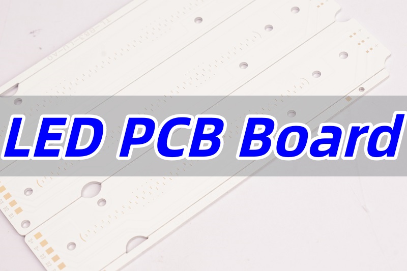
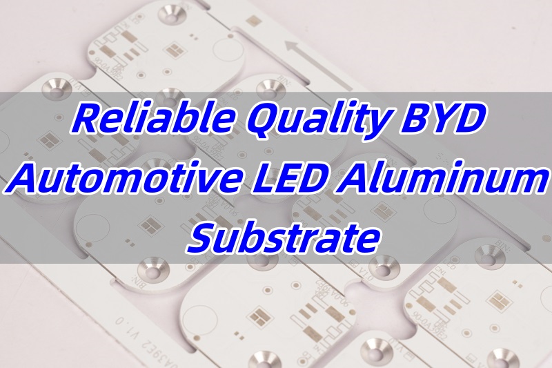
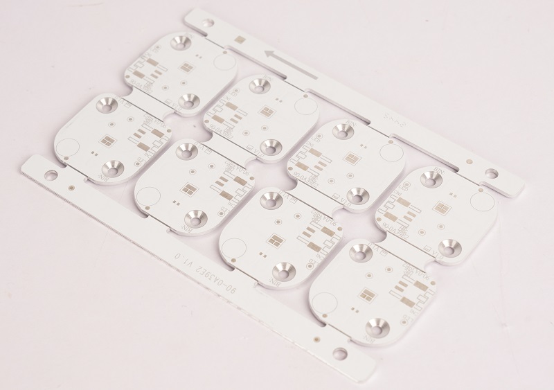
LED PCB board is the backbone of modern lighting. The blog shares valuable points on the design, construction, testing, and diverse applications of LED PCB boards, including differences between power ratings, features of LED strip PCBs, and guidance for sourcing high-quality prototypes.
Are there major challenges hindering your LED PCB board project?
Improper thermal design causes overheating and shortens lifespan?
Inconsistent manufacturing quality, such as uneven brightness, flickering, or varying lifespans?
Design difficulties and long production cycles?
High-quality LED PCB boards are costly, and your customers choose cheaper products, potentially sacrificing quality?
Here’s how we tackle the issues mentioned above:
Optimized Thermal Management: Using metal-core PCBs (MCPCB) and advanced thermal design to improve heat dissipation efficiency.
Enhanced Quality and Consistency: Employing advanced manufacturing equipment and strict quality control processes to ensure product uniformity.
Technical Support and Project Management: Providing technical support and project management services to guide clients through the entire process from design to delivery.
Cost and Performance Balance: Offering high cost-performance solutions that balance budget constraints with product performance.
As a PCB light board manufacturer, EBest Circuit (Best Technology) provides custom LED PCB, SMD LED PCB board prototypes, LED PCB board design, mass production, LED PCB board 12v assembly, LED PCB Strip box build service. We have our own metal core PCB factory, responsible for expediting your delivery time, quality control, and full process coordination. You don’t need to waste time and money to communicate with different factories. Since you cooperate with EBest Circuit (Best Technology), which is a one-stop PCB and PCBA factory. If you have any doubts or requirements about LED PCB board material selection, LED PCB board prototypes, or LED PCB fabrication, just feel free to make contact with us through sales@bestpcbs.com.
What is LED PCB Board?
An LED PCB board (Light Emitting Diode Printed Circuit Board) is a specialized circuit board designed to mount, connect, and power LED components. It not only provides electrical pathways but also supports the LEDs mechanically and manages heat efficiently, ensuring stable illumination and extended lifespan. In essence, LED PCB boards form the backbone of modern lighting systems, supporting everything from small LED PCB boards to large-scale LED display PCB boards.
Key Components and Structure
Substrate: The base material, which can vary from standard FR4, aluminum, or ceramic, is chosen based on thermal management requirements. For instance, aluminium PCB boards for LED are widely used in high-power applications due to their excellent heat dissipation.
Copper Layer: Conductive traces transmit power from the input terminals to each LED. The thickness and layout of the copper layer determine current carrying capacity and light output stability.
Solder Mask: This protective layer prevents short circuits and oxidation while providing a reliable surface for soldering LEDs and other components.
Pads: Areas where LEDs and resistors are mounted, ensuring both electrical connectivity and mechanical stability.
Surface Finish: Treatments like ENIG or HASL enhance solderability and protect copper traces.
Why It’s Important / Core Advantages
Efficient Thermal Management: With metal-core designs like MCPCB or aluminium LED PCB boards, heat generated by high-power LEDs is dissipated effectively, preventing overheating.
Enhanced Brightness and Efficiency: Optimized circuitry reduces energy loss, improving luminous efficiency for LED strip PCB boards, RGB LED PCB boards, and other configurations.
Extended Lifespan: Proper heat control and reliable construction reduce the risk of premature failure, especially in LED ceiling light PCB boards or LED tube light PCB boards.
Flexible Design Options: Whether for custom LED PCB boards or high-density SMD LED PCB boards, layouts can be tailored to fit specific applications.
Difference from FR4
While FR4 is a common material for standard circuit boards, offering low cost and good insulation, its thermal conductivity is limited.
In contrast, LED PCB boards often use metal or ceramic substrates to handle higher power and manage heat efficiently, crucial for maintaining consistent brightness and long-term reliability. The choice of board material—be it aluminium LED PCB board, LED PCB board material for high-wattage setups, or FR4 for low-power designs—directly affects thermal performance, current handling, and overall efficiency.
Main Types
Single-Sided LED PCB Boards: Simple layout with copper traces on one side, suitable for basic LED applications.
Double-Sided LED PCB Boards: Copper traces on both sides, often used for more complex LED boards.
Multilayer LED PCB Boards: Three or more layers, ideal for high-power or dense LED circuit boards.
Flexible LED PCB Boards: Can bend for curved installations, perfect for LED strip PCB boards or wearable lighting.
Metal-Core LED PCB Boards (MCPCB): High heat dissipation, commonly used for LED bulb PCB boards or LED display PCB boards.
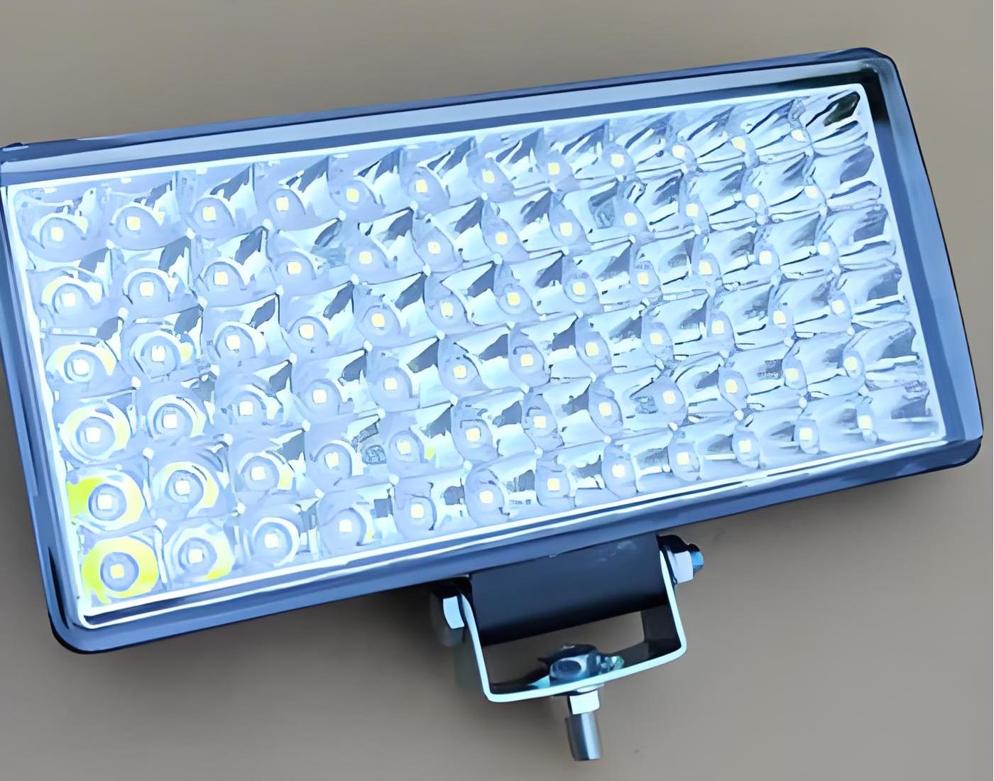
LED PCB boards are used across a variety of lighting scenarios including residential and commercial illumination, automotive headlights, industrial lighting, LED display panels, and emergency lighting solutions like LED emergency light circuit PCB boards.
What is SMD LED PCB Board?
SMD stands for Surface-Mount Device, a critical distinction in modern electronics. An SMD LED PCB board refers to a printed circuit board where SMD LEDs are directly mounted and soldered onto the board surface using Surface-Mount Technology (SMT). Unlike traditional through-hole LEDs, which require long leads to pass through the PCB, SMD LEDs are compact, flat, and attach directly to the board, making the board thinner and more space-efficient.
Why SMD is a Big Deal
Size and Density: SMD LEDs are smaller and lighter, enabling designers to place more diodes on a limited area. This high-density arrangement is essential for LED PCB strips, LED display PCB boards, and high-resolution backlighting. Miniaturization allows slim and lightweight designs for products like LED ceiling light PCB board replacements.
Performance and Light Quality: SMD LEDs often offer wider viewing angles (120°–180°), higher luminous efficiency, and more color versatility, including RGB LED PCB boards. They provide smooth, even light output for LED light PCB boards in commercial or residential lighting applications.
Manufacturing and Cost Efficiency: SMD LEDs are ideal for automated assembly with high-speed pick-and-place machines. This reduces labor costs, increases production consistency, and supports cost-effective manufacturing of custom LED PCB boards or LED 12V PCB boards.
Design Flexibility: The small size allows for complex and compact LED PCB board designs, making it possible to integrate high-power LEDs like LED PCB board 100W or LED PCB board 18W into versatile lighting solutions.
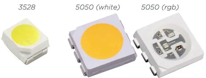
Common SMD LED Types and Identification
2835, 3528: Widely used for general lighting in LED strip PCB boards.
5050, 5060: Larger packages for higher brightness or RGB LED PCB boards.
3014, 4014: Ultra-thin SMDs for backlighting in LED TV PCB boards or monitors.
COB (Chip-on-Board): Though not a traditional SMD, it’s a related technology where multiple chips are integrated on a single PCB to form a large, uniform light surface.
Differences Between COB LED Strips and SMD LED Strips
COB and SMD LED strips differ in light efficiency, flexibility, and lifespan.
Light Quality:
COB LED strips use chips embedded in a gel-like material, producing a more uniform and soft light.
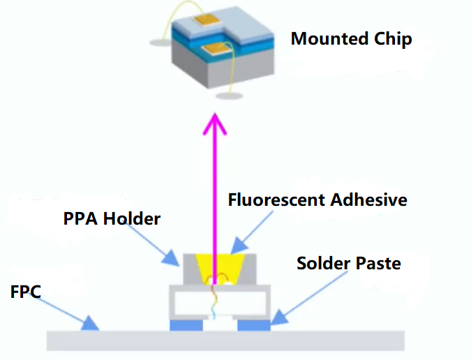
SMD LED strips have LEDs directly mounted on the PCB. When lit, the individual LEDs are visible, creating a noticeable dot effect. Fewer LEDs increase this dot effect and can create dark spots.
Flexibility:
COB strips are more flexible, allowing designers to shape them freely.
SMD strips can protrude at corners due to the mounted LEDs, limiting design flexibility.
Thermal Management and Lifespan:
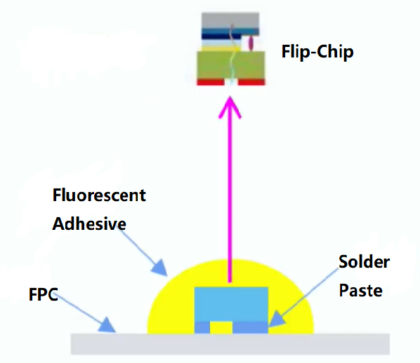
COB LED strips use flip-chip technology, offering better heat dissipation and longer lifespan.
SMD LED strips use packaged chips/mounted chips, which have higher thermal resistance and reduced longevity.
Key Applications
Consumer Electronics: Backlighting for smartphones, tablets, laptops, and LED light PCB boards for compact devices.
High-End Lighting: Panel lights, LED tube light PCB boards, smart bulbs, and modern automotive lighting systems.
Display Technology: Indoor and outdoor full-color LED screens, including small-pitch LED display PCB boards (P0.9, P1.2, etc.).
Decorative Lighting: LED PCB strips, RGB strips, and smart lighting fixtures.
Practical Takeaways for Buyers
Selection Tips: When choosing SMD LEDs, consider package type (e.g., 2835 for higher efficiency than 3528), color rendering index (CRI), and color temperature.
Reliability: Since SMD LEDs have exposed solder points, PCB thermal design and production quality are critical to longevity, particularly for high-power applications like aluminium PCB board for LED or LED PCB board 100W setups.
To wrap things up, SMD LED PCB boards are the modern standard in LED technology. The key advantage lies in the surface-mount method, which allows miniaturization, high efficiency, and cost reduction. SMD designs have driven the evolution of LED lighting and displays, from LED ceiling light PCB board replacements to high-resolution LED display PCB boards, making them indispensable in today’s electronics and lighting industry.
What is the Difference: LED PCB Board 100W vs 18W?
The difference between a LED PCB board 100W and an 18W board goes far beyond brightness—it is essentially a battle in thermal management. The 100W design focuses on how to dissipate huge amounts of heat, while the 18W design emphasizes efficient and reliable illumination.
Think of it like this: the 18W board is a family car engine—adequate, reliable, and simple. The 100W board, however, is a high-performance sports car engine—demanding in heat dissipation, power supply, and materials. Their requirements are on completely different scales.
A Side-by-Side Breakdown
Thermal Management and Heat Dissipation (Core Difference)
18W: Heat generation is moderate. Small aluminium PCB boards for LED can dissipate heat through their surface area and simple enclosures (like plastic housings). The thermal design is straightforward.
100W: Generates massive heat. Requires large metal heatsinks, often die-cast aluminum, with additional cooling fins. The PCB itself is only part of the thermal system. Poor heat management can lead to immediate LED degradation or failure.
PCB Design and Materials
18W: Standard thermal conductivity of the aluminum or FR4 substrate suffices. Copper traces are relatively simple.
100W: High thermal conductivity aluminum or even ceramic substrates are needed. Copper layers must be thick to carry large currents. Circuit layout prioritizes thermal balance to prevent hotspots.
LED Components and Layout
18W: Uses fewer standard SMD LED PCB boards (like multiple 2835 LEDs) to achieve sufficient brightness.
100W: Needs high-power, expensive constant-current drivers. Higher input/output voltage and current require components with higher voltage tolerance and current-carrying capacity.
Safety and Reliability
18W: Low risk; failure usually manifests as gradual light decay.
100W: High safety risk. Involves high voltage and temperature. Requires superior insulation, fire-resistant materials, IP-rated housings, and multiple protections (over-voltage, over-temperature, short-circuit).
Where They Are Used
18W PCB boards: Mainstream for home and commercial lighting—LED ceiling light PCB board replacements, panel lights, desk lamps, and LED PCB strips. Emphasis on cost-effectiveness, compactness, and aesthetics.
100W PCB boards: Industrial, outdoor, and specialized lighting—high-mast street lights, industrial floodlights, plant grow lights, stadium lighting, and large searchlights. Priority is maximum luminous output and reliability; size and cost are secondary considerations.
Actionable Advice for Buyers
Don’t focus solely on wattage: Pay attention to heat dissipation (heatsink design), luminous flux (lumens), and efficiency (lm/W).
Cost Difference: The total system cost for a 100W solution (PCB + heatsink + high-power driver) is far more than five times that of an 18W board—often tens of times higher.
Selection Warning: Never use a 100W LED PCB in a confined space or without proper cooling—it risks severe overheating or fire. The 18W boards are much safer and flexible.
All in all, the difference between 100W and 18W LED PCB boards is a classic example of how quantitative changes lead to qualitative transformations. The jump in power requires fundamental changes in PCB materials, layout, heat management, LED selection, and driver design, reshaping the board’s application, safety, and performance. Choosing the right wattage is not just about brightness—it’s about engineering a complete, reliable LED solution.
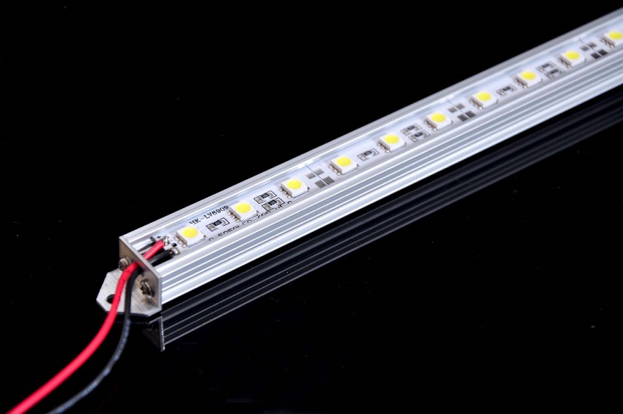
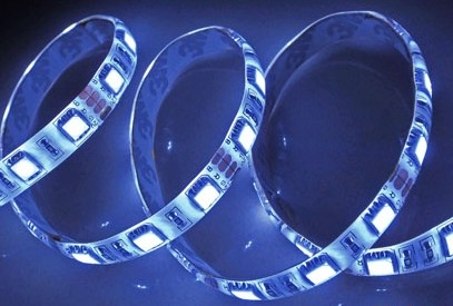
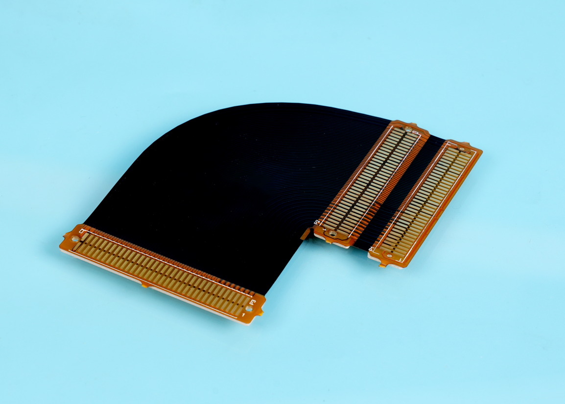
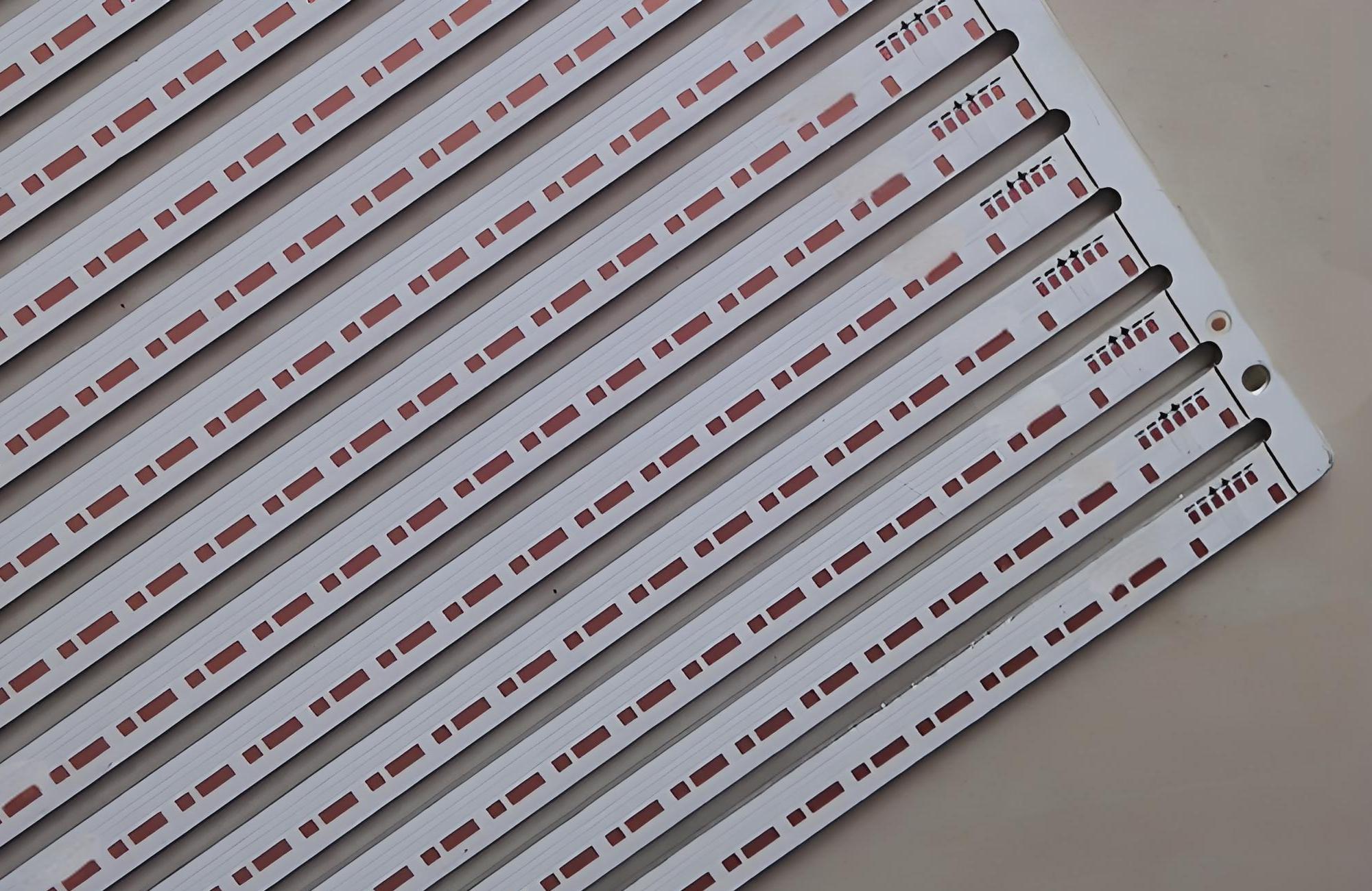
What are the Features of LED Strip PCB Board?
LED strip PCB boards have become a popular choice for modern lighting due to their flexibility, efficiency, and wide design options. From residential decoration to large-scale commercial projects, they combine advanced PCB technology with innovative LED packaging to deliver stable performance and long service life. Understanding their structure, materials, voltage ranges, and chip types is essential for choosing the right solution for different applications.
1. Base Materials of LED Strip PCB Board
Rigid PCB board: Made with solid PCB substrates, offering better heat dissipation and durability, suitable for high-end lighting applications.
Flexible FPC board: Lightweight and bendable, ideal for installations in narrow or irregular spaces.
2. Classification by Structure
Hard LED Strips: Easy to mount, quick heat dissipation, and reliable for projects requiring long service life.
Soft LED Strips: Ultra-thin and flexible, can be folded or combined freely, widely used in versatile applications.
3. Voltage Options
High-Voltage Strips: Capable of long-distance lighting (50–100 meters) with a clean appearance, though slightly lower in safety.
Low-Voltage Strips: Typically 12V/24V, safer for residential and commercial lighting, though limited in length (usually ≤10 meters).
4. LED Chip Specifications
Popular models include 3528, 2835, 5050.
Packaging size and chip count affect brightness, power consumption, and cost (e.g., 5050 brightness ≈ 3 times of 3528).
5. Key Features
Consistent LED spacing for soft and balanced lighting.
Cuttable design to meet custom length requirements.
Adhesive backing for quick and simple installation.
Slim and compact, saving space and fitting multiple scenarios.
6. Application Scenarios
Ambient and decorative home lighting.
Commercial displays and advertising light boxes.
Stage lighting, entertainment venues, and outdoor landscape illumination.
Automotive interiors and creative DIY projects.
LED strip PCB boards combine versatile designs, safe voltage options, and advanced LED chip technologies to deliver reliable lighting solutions. Whether used in residential decoration, commercial displays, or large outdoor projects, they provide efficiency, ease of installation, and long-lasting performance. For businesses and engineers, understanding the materials, structures, and technical features helps in selecting the most suitable type of LED strip PCB board for specific needs.
How to Make LED PCB Board?
Making an LED PCB board is a precise process that requires careful attention to circuit design, heat management, and component assembly to ensure stable and reliable lighting performance. While rigid LED boards and flexible LED strips (FPC) differ slightly, the core manufacturing steps are largely similar.
1. Selecting Base Materials
Rigid PCB Board: Made of FR4 or aluminum substrates, offering excellent heat dissipation and mechanical strength, suitable for high-power LED rigid strips.
Flexible FPC Board: Thin and bendable, ideal for installation in tight or irregular spaces, used for flexible LED strips.
2. Copper Lamination
Copper is laminated onto the substrate to form conductive layers.
Copper thickness is chosen based on current requirements; high-power LEDs require thicker copper to prevent overheating.
3. Circuit Etching
Unwanted copper is removed to form precise circuit patterns.
Correct line width and spacing ensure even current distribution and prevent voltage drop or short circuits.
4. Solder Paste Application
Solder paste is applied to pads to prevent shorts and protect copper traces from oxidation.
This layer also ensures reliable soldering for LEDs and resistors.
5. Pad Surface Finishing
Pads can be treated with ENIG, OSP, or other finishes to ensure strong and reliable solder joints.
6. Component Placement
LED chips, resistors, and other components are placed using automated pick-and-place machines.
Flexible LED strips commonly use 12, 15, 18, 24, or 30 LEDs per segment.
Key considerations: correct LED polarity, resistor value, and accurate component positioning to ensure uniform brightness.
7. Reflow Soldering
The assembly is heated in a reflow oven to melt the solder paste and fix components.
Temperature control is critical: too low causes cold solder joints; too high can damage FPC or cause warping and solder balls.
8. Inspection and Testing
Visual Inspection: Check for misaligned components, solder bridges, or shorts.
Electrical Testing: Verify LEDs operate correctly, current is stable, and voltage meets specifications.
9. Waterproofing (Optional, LED Strip Finished Stage)
Different waterproofing methods vary in encapsulation method and material:
Epoxy Coating: A thin layer of epoxy is applied to the LED surface; simple but offers limited protection.
Silicone Tubing: LEDs are inserted into silicone tubes, with ends sealed; flexible and suitable for light water resistance.
Solid Encapsulation (U-channel + Resin): The strip is placed in a U-shaped channel, then filled with resin; strong structure and good waterproofing.
Potting (PU or Epoxy Resin): The entire strip is encapsulated in resin, providing maximum weather resistance and protection.
10. Aging, Testing, and Packaging
Completed PCB or LED strips undergo aging tests to ensure long-term reliability.
LED strips are typically packaged in 5-meter rolls using anti-static and moisture-proof materials for safe storage and shipping.
To sum up, every stage of LED PCB board production requires precision—from base selection, copper lamination, and circuit etching to component placement and reflow soldering. Flexible strips also require considerations for bendability and space adaptability. Strict manufacturing standards combined with MES system tracking ensure high-quality, reliable LED PCBs widely used in home, commercial, automotive, and decorative lighting applications.
How to Build a LED PCB Board Design Step by Step?
Designing a new LED PCB board requires careful planning and attention to detail. A well-designed board ensures optimal light output, thermal performance, and reliability. Below is a step-by-step guide to LED PCB design:
1. Define Design Goals
Before starting, define the essential goals:
Target light output (lumens)
Operating voltage (commonly 12V or 24V)
Expected lifetime and reliability
Thermal management requirements
2. Select Materials
Choose base materials based on application:
Aluminum PCB: Excellent for high-power LEDs, provides superior heat dissipation.
FR4 PCB: Cost-effective, suitable for low-power LED applications.
Flexible FPC: Ideal for soft LED strips or irregular shapes.
3. Circuit Layout
Use CAD software to lay out the PCB traces and LED positions:
Ensure proper spacing between copper traces to prevent shorts and overheating.
Plan thermal paths for heat dissipation under each LED pad.
Follow industry-standard design rules for trace width:
For current carrying traces, the IPC-2221 formula is often used:
Trace Width (W) = (I / (k · (ΔT)0.44))1/0.725 where I is current (A), ΔT is allowed temperature rise (°C), k is a constant based on copper thickness.
4. Layer and Drill Planning
Decide the number of layers:
Single-layer PCB: simplest, low power, low cost.
Double-layer PCB: standard for most LED boards.
Multi-layer PCB: for complex designs or higher currents, often 4–6 layers.
Drill locations should match LED lead holes and vias for thermal and electrical connection.
5. Thermal Management
LED performance depends heavily on heat control:
Use thermal vias under high-power LEDs to conduct heat to the metal core.
Keep copper thickness and pad size sufficient to carry required current.
6. Simulation and Verification
Before fabrication:
Simulate current flow and temperature rise to detect hotspots.
Check trace width and spacing using design rule checks (DRC) in CAD software.
Review LED polarity, pad sizes, and via placements to avoid assembly issues.
7. Prototype and Testing
Build a prototype and test:
Measure brightness, voltage, and current.
Verify temperature under load.
Check electrical continuity and insulation.
Adjust design as needed before mass production.
8. Final Checks
Ensure the PCB design meets the following:
All LED pads have correct polarity and spacing.
Trace width sufficient for current without excessive temperature rise.
Thermal paths and metal core areas optimized for heat dissipation.
Layer stackup and drill positions correctly defined.
Following these steps ensures a robust LED PCB design that performs reliably. EBest Circuit (Best Technology) engineers provide professional design review and optimization, reducing redesign costs and improving manufacturing yield.
How to Test LED PCB Board?
Testing an LED PCB board is not just a formality—it’s a critical step to ensure safety, performance, and long-term reliability. Testing ensures LED PCB boards are safe, fully functional, and durable under real operating conditions. It should cover incoming materials, in-process checks, and final inspection, though clients usually focus on final inspection and random sampling to verify quality.
1. Step-by-Step Testing Process
Step 1: Visual Inspection
Objectives:
Check PCB cleanliness, surface scratches, burns, or mechanical damage.
Confirm LED orientation, model, and position; no reverse polarity or missing LEDs.
Inspect solder joints: full, smooth, without cold solder, bridges, or solder balls.
Tools:
Magnifying glass or microscope (for high-density boards)
Direct visual inspection
Why it matters: Early detection of physical defects prevents functional failure after power-up.
Step 2: Electrical Performance Testing
Key Tests:
1. Continuity & Short-Circuit Test:
Use a multimeter to verify all circuits are connected properly.
Detect shorts or open circuits before powering the board.
2. Insulation & Hi-Pot Test:
Apply high voltage to check isolation between conductors.
Critical for safety in high-voltage designs.
3. Power-On Test:
Apply rated voltage and current.
Check all LEDs for full brightness; no dead or flickering LEDs.
Measure brightness, color temperature, and CRI; RGB boards should show consistent color mixing and proper signal response.
Step 3: Optical Performance Testing
Objectives:
Luminous Flux (Lumens): Ensure total light output meets specifications.
Color Temperature & Color Coordinates (CCT): Verify light color accuracy (e.g., 2700K warm white, 6000K daylight).
Color Consistency: Check for batch-to-batch variation; ensure uniform appearance across multiple boards.
Tools:
Integrating sphere or light measurement equipment
Step 4: Thermal Performance Testing
Objectives:
Measure LED junction temperature (Tj) under rated load using thermocouples or thermal imaging.
Calculate thermal resistance (Rθ) and confirm temperature rise is within LED specifications:
Rθ = (Tjunction_max – Tambient) / Ptotal
Where Tjunction_max is maximum allowed junction temperature, Tambient is ambient temperature, and Ptotal is total power.
Monitor brightness decay after continuous operation (e.g., 30 minutes) to assess thermal stability.
Why it matters: High junction temperatures accelerate LED degradation and reduce lifespan. Controlling thermal performance ensures reliability.
Step 5: Environmental & Reliability Testing
Burn-In Test:
Continuous operation at rated or slightly higher current for 24–72 hours.
Screens out early failures (“infant mortality”) before shipping.
Optional Stress Tests (based on application):
Vibration (for automotive LED boards)
Thermal cycling or shock (outdoor / IP-rated applications)
Humidity or waterproof tests
These ensure LEDs meet long-term durability requirements.
2. Practical Guide for Clients
What to request from suppliers:
Detailed Test Reports / Certificates of Analysis (COA)
Data for burn-in, optical output, thermal performance, and electrical safety
Sampling Strategy:
Inspect incoming shipments using standards like AQSL II
Focus on visual checks, power-on tests, and basic electrical testing
Recommended Tools:
Essential: Multimeter, adjustable DC power supply, magnifying lens
Advanced: Thermal camera, integrating sphere
Handling Defects:
Define Acceptable Quality Limit (AQL)
Establish clear rejection and return policies
In summary, a rigorous LED PCB testing workflow ensures that boards are safe, functional, and durable. By combining visual, electrical, optical, and thermal inspections with environmental stress testing, clients can confidently verify product quality, reduce field failures, and choose reliable suppliers.
Where to Get an LED Light PCB Board?
Choosing the right supplier is often the hardest step. Some buyers face issues with poor quality, late shipping, or inadequate technical support.
Quality Assurance: EBest Circuit (Best Technology) solves these pain points with certified systems like ISO 9001, ISO 13485, IATF 16949, and AS9100D. All our manufacturing process are fully compatible with these standard.
Fast Prototypes: We offer high-quality and quick prototypes. If you have cooperated with us, you will enjoy our strong engineering support. All the prototypes are without MOQ requirements.
Advanced system and equipment: Using MES traceability, we track each part of the process, giving clients excellent quality in long-term supply. And every year, we will purchase cutting-edge machines to meet the higher volume order needs and the diverse project requirements of different customers.
In closing, whether it is an LED PCB board 12V, an LED PCB Strip, or custom LED PCB, EBest Circuit (Best Technology) delivers both small and large runs without delay.
What are the Applications of LED PCB Boards?
LED PCB boards are no longer just for basic lighting. They now enable precision, flexibility, and energy savings across virtually every sector that requires controlled light. From industrial lamps to high-tech displays, LED boards drive innovation and efficiency, influencing both technical choices and commercial strategy.
1. Detailed Applications by Sector
1.1 Lighting Applications
General & Commercial Lighting: Indoor panel lights, downlights, bulbs, tubes, industrial and commercial luminaires, and street lamps. Key considerations: cost efficiency, luminous efficacy, lifespan, and color rendering (CRI).
Agricultural Lighting: plant growth LEDs targeting specific spectra (red and blue). Focus: spectral accuracy, waterproofing, high PPF/PPFD for plant growth efficiency.
1.2 Display & Backlight Applications
Information Displays: outdoor billboards, stadium screens, traffic signage, financial tickers. Focus: high brightness, fast refresh, weatherproofing, long-distance visibility.
Consumer Electronics Backlight: LCD TVs, monitors, laptops, tablets. Focus: thin form factor, uniform light distribution, advanced Mini/Micro LED technologies.
High-End Commercial Displays: indoor small-pitch LED screens for command centers, meeting rooms, broadcasting. Focus: pixel density, color consistency, low brightness/high gray performance.
1.3 Signaling & Indication
Traffic Signals: traffic lights, railway indicators. Focus: ultra-reliable operation, brightness, precise wavelength for visibility and compliance.
Status Indicators: appliances, industrial equipment, network routers. Focus: compact size, long lifetime, low power consumption.
1.4 Emerging & Innovative Applications
UV/IR LEDs: UV for curing (3D printing, nail art, ink printing) and sterilization; IR for night vision and facial recognition. Focus: wavelength-specific power, effective thermal management.
Wearables & Smart Devices: smart wristbands, health monitors, flexible luminous textiles. Focus: flexible PCB, low power consumption, lightweight design.
Automotive & Smart Transportation: beyond lighting, including LiDAR and optical sensing. Focus: precision optics, high-speed pulse performance.
2. Insights and Decision-Making Guide
Technical Requirements Comparison Across Applications:
Thermal Management: low for status indicators, extreme for high-power street lights and UV curing devices.
PCB Type Selection: rigid (industrial/street lights), FPC (flexible strips), MCPCB (metal-core for automotive), ceramic (UV/IR for heat-intensive applications).
Performance Priorities: brightness, color accuracy, lifespan, cost – weighted differently per application.
Communicating with Suppliers: Do not just say “I need a LED board.” Specify the end-use scenario (e.g., “outdoor plant growth light”), so suppliers can recommend power rating, spectral design, IP rating, and thermal solutions accurately.
Trends and Future Outlook:
Mini/Micro LED: driving next-generation displays, requiring high PCB precision.
Smart Lighting & IoT Integration: higher integration with sensors and controllers.
Efficiency & Sustainability: ongoing improvements in luminous efficacy and environmentally friendly materials.
To conclude, LED PCB boards serve as a strategic technology platform across multiple sectors. By mapping applications, understanding technical requirements, and analyzing business value, clients can make informed decisions on design, procurement, and market opportunities. This approach helps identify where and why LED PCBs are used, enabling optimized product strategies and competitive advantage.
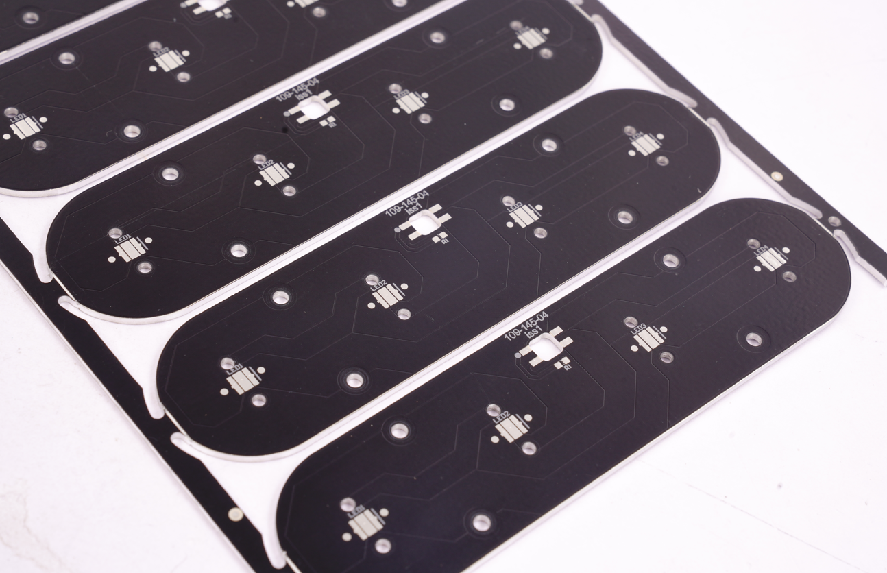
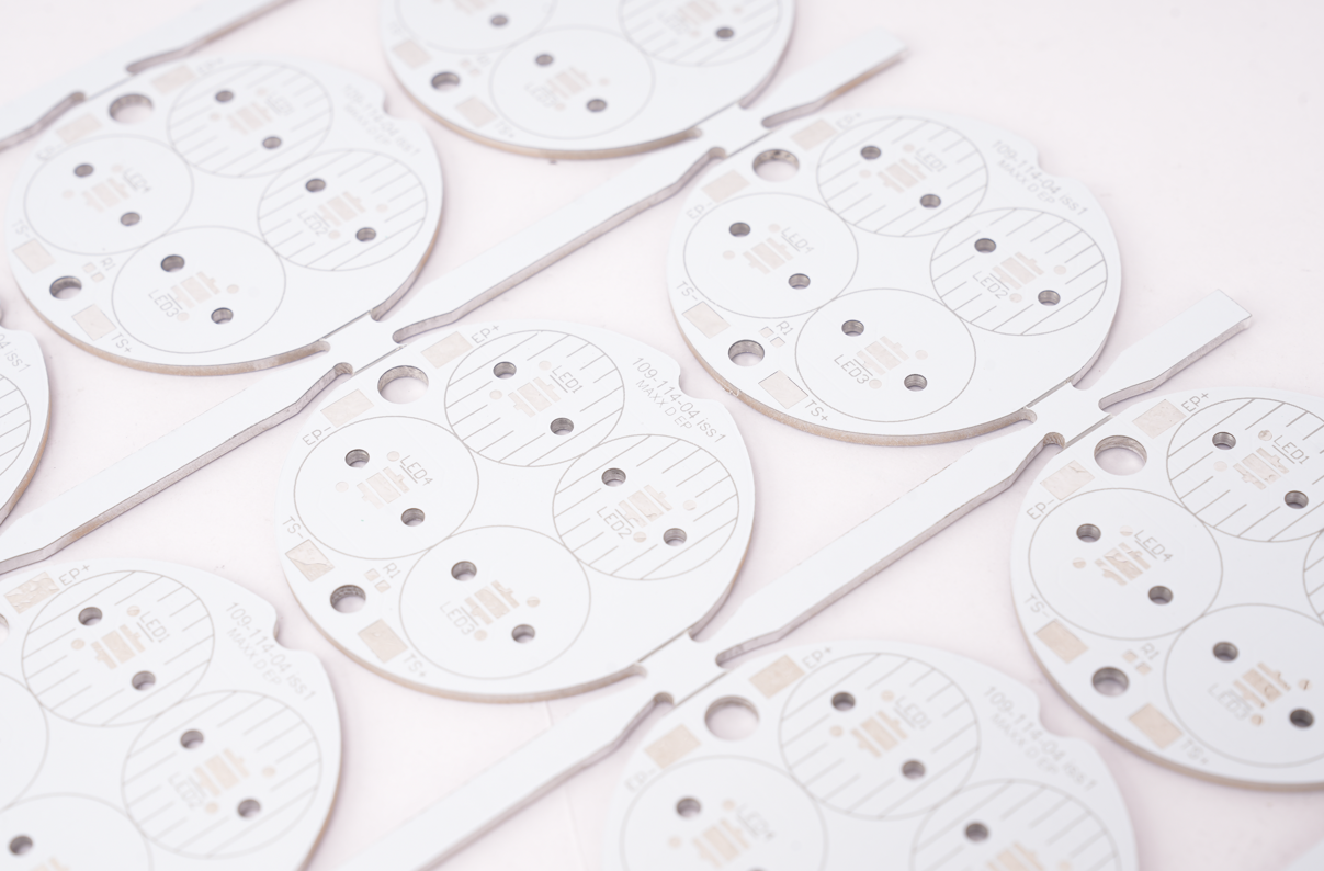
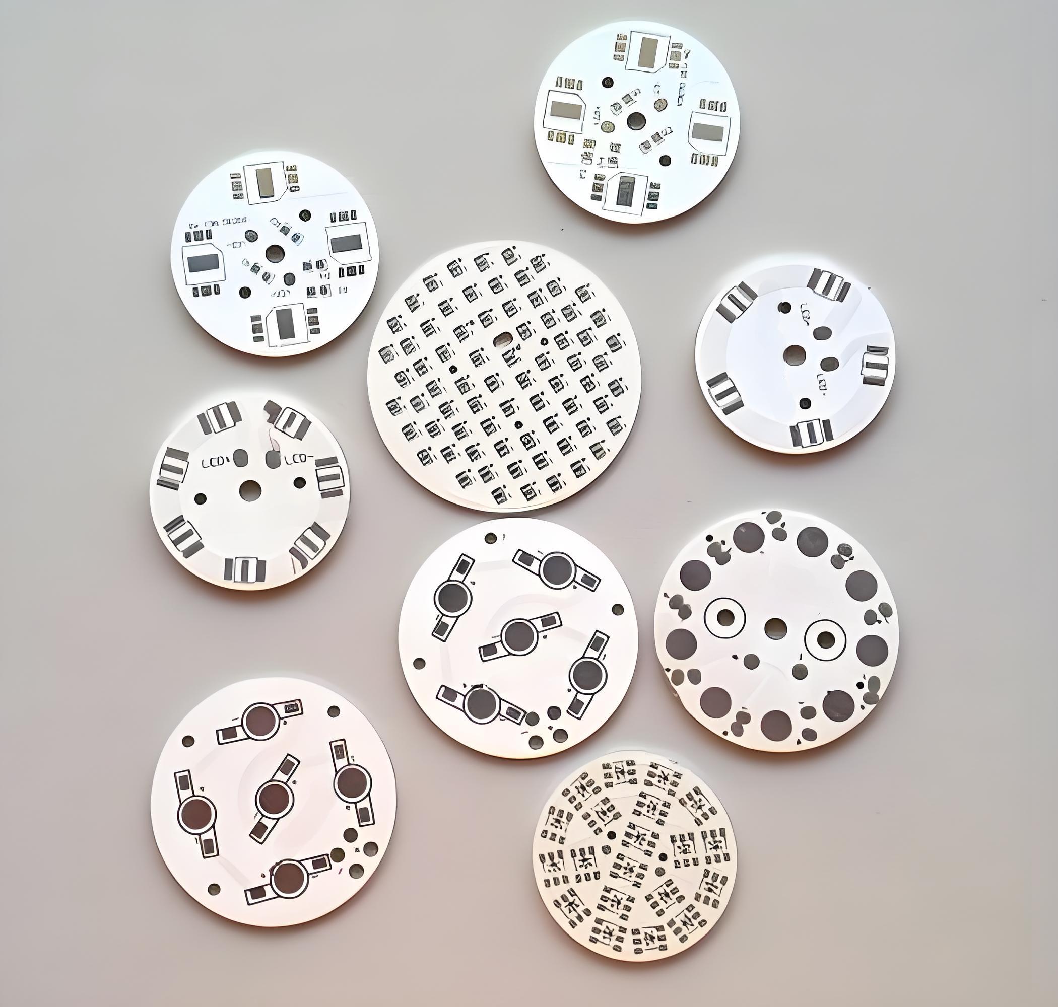
Case of PCB Light Board in EBest Circuit (Best Technology)
Here are some cases EBest Circuit (Best Technology) completed for our customers. These LED PCB boards are widely applied in different lighting projects, from outdoor high-power lamps to indoor decorative lights. Their design and performance directly support brightness, stability, and long lifespan in real applications.
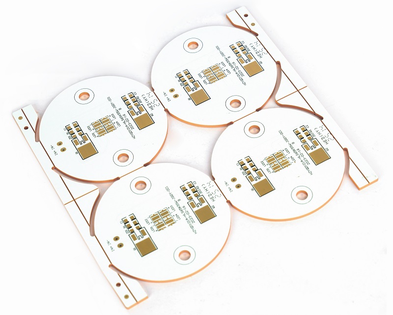
Double-Sided Aluminum PCB
Finished board thickness: 1.6mm±10%;
Thermal conductivity: 3W;
Copper thickness: 1OZ;
Solder mask: Black with white legend;
Surface finish: Lead-free HASL;
This type of PCB is commonly used in high-power LED floodlights, street lamps, and stadium lights. Its double-sided structure supports complex circuit routing, while the aluminum base helps manage high thermal loads. In outdoor lighting projects, such as highway lighting or public square illumination, these boards provide both durability and efficiency.
Single-Sided Double-Layer Copper PCB
Copper base thickness: 1.3mm;
Copper thickness: 1/1OZ;
Thermal conductivity: 3W/m.k;
Finished board thickness: 1.60mm±10%;
Solder mask: Black with white legend;
Surface finish: OSP;
This copper-based PCB is often chosen for LED power supply modules, industrial lighting fixtures, and high-brightness spotlights. The excellent conductivity of copper provides stable current flow, which is important in commercial lighting systems, stage spotlights, and smart control LED panels. It delivers both high brightness and reliable performance under continuous use.
Single-Sided Double-Layer Aluminum PCB:
Aluminum base thickness: 1.50mm;
Copper thickness: 0.5/0.5OZ;
Thermal conductivity: 3W/m.k;
Finished board thickness: 1.85mm±10%;
Solder mask: Black with white legend;
Surface finish: OSP;
This board is suitable for LED panel lights, downlights, tube lights, and automotive interior lamps. The aluminum base ensures strong heat dissipation, while the dual copper layers maintain circuit stability. It is widely used in office ceiling lighting, residential decorative lamps, and car dashboard backlight systems, where energy efficiency and uniform brightness are required.
In a nutshell, LED PCB boards are more than just carriers of light. They balance power, heat, and cost in ways that define product success. Yet, buyers often face real pain points: lack of design support, poor heat control, or unreliable supply. EBest Circuit (Best Technology) meets these challenges with certified processes, strong engineering, and a customer-first mindset. By offering LED PCB board design advice, reliable testing, and professional service through all process, we give clients the trust they need. A warm welcome to get in touch with us via sales@bestpcbs.com for a creative solution.
As a LED MCPCB Manufacturer, We are proud to provide a wide variety of MCPCBs for the lighting world. With over 19 years of experience in designing and manufacturing MCPCBs, we take pride in being your one-stop supplier.
As a trusted supplier, we hold certifications including UL, ISO13485, ISO9001, IATF16949 and SGS, enabling us to meet the high standards of clients across Europe, America, Israel, India, and so on. Explore our services and let us help you fulfill your MCPCB needs.
Are you looking for LED MCPCB Manufacturer? Do you have any questions?
What types of MCPCBs do you mainly produce?
Do you support customized designs?
What is the typical delivery time? Do you offer expedited service?
What after-sales service and technical support do you provide?
As a MCPCB manufacturer with 19+ years of experience, BEST Technology can tell you:
Based on metal substrate type, we offer copper, copper-aluminum, aluminum, and steel substrates. Based on product structure, we offer thermal and electrical separation MCPCBs, rigid-flex MCPCBs, and single- and double-sided multilayer MCPCBs.
We offer one-stop customized solutions from design to production.
Standard delivery time is 5-10 business days; we also offer expedited service, and urgent boards can be shipped out within 24 hours!
Quality inspection and returns and exchanges are included. We also provide design-for-manufacturing (DFM) advice, technical consulting, and troubleshooting services.
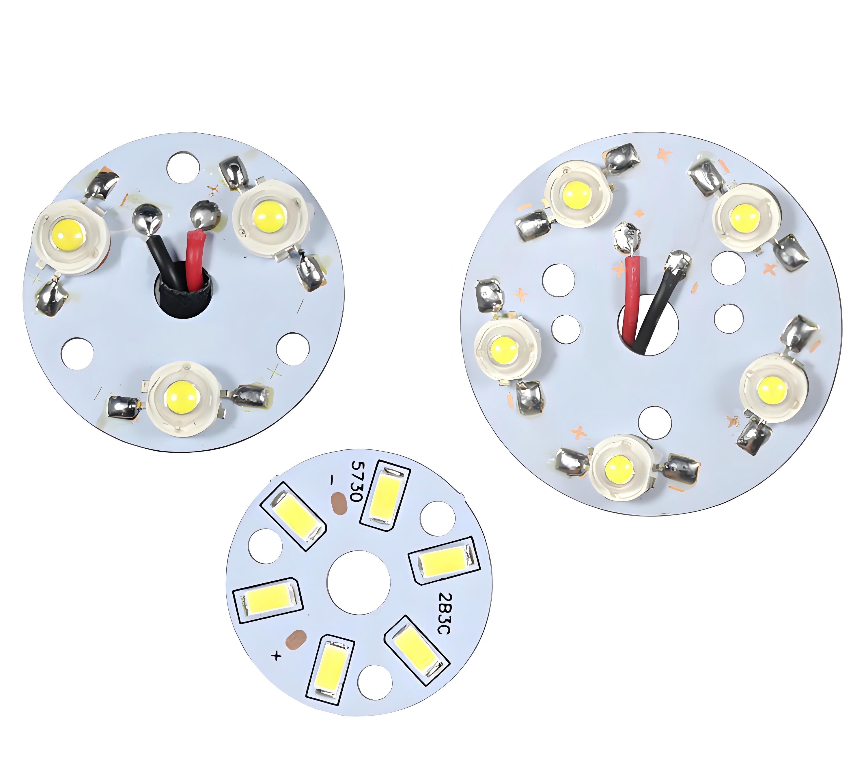
What is MCPCB LED?
An MCPCB LED is a light-emitting diode mounted on a Metal Core Printed Circuit Board. Unlike a standard circuit board, an MCPCB uses a metal plate as the base. This metal core, usually aluminum or copper, moves heat away from the LEDs fast. Heat is the main reason LEDs fade or fail. A board that spreads heat keeps them bright and strong.
MCPCB LEDs appear in almost every modern lighting product. LED panels for offices, car headlights, medical lamps, and industrial floodlights all rely on this design. The solid metal base creates a powerful thermal path. That means longer life, steady color, and reliable brightness.
Which board is better for LEDs: MCPCB or standard FR-4?
FR-4 is a fiberglass and epoxy laminate. It works for many electronics. But LEDs run hot and need better heat transfer.
As a MCPCB led manufacturer, BEST Technology can tell you the advantages of MCPCB:
Metal base moves heat away quickly.
LEDs stay at a safe operating temperature.
Brightness and color remain stable for years.
FR-4 costs less for simple circuits. Yet for high-power LED lights, it can become a weak link. Over time heat builds up. That can reduce LED life and cause early dimming.
When a product demands long service and high brightness, MCPCB is the better choice. The small extra cost pays back through fewer failures and less maintenance.
What is a Metal Core PCB and why do LEDs need it?
A Metal Core PCB has a solid metal plate inside the board. Most often that plate is aluminum. Some high-performance designs use copper or a mix of alloys.
The structure is simple but powerful. A thin dielectric layer separates the copper circuit from the metal base. This dielectric must be thermally conductive yet electrically insulating.
LEDs convert electricity into light. That process produces heat. If heat stays near the LED chip, performance drops. Light output falls, and lifetime shortens.
The metal core solves this. Heat flows fast from the LED junction through the dielectric into the metal base. From there it moves to a heat sink or the surrounding air. This keeps the LED at an optimal temperature.
With a cooler junction, the LED can handle higher current and stay bright. This is why china mcpcb led board manufacturers focus on precise thermal design.
How does the LED PCB assembly process work for MCPCBs?
Building an LED MCPCB involves several careful steps. Professional led pcb assembly lines follow strict procedures:
Material Preparation: Aluminum or copper base plates are cleaned and coated with a thin dielectric.
Circuit Imaging and Etching: Copper foil is laminated and patterned. Chemical etching forms the circuit traces.
Solder Mask and Surface Finish: A heat-resistant solder mask protects the copper. ENIG or OSP finishes create strong solder joints.
Component Placement: High-speed pick-and-place machines set LEDs and other parts accurately.
Reflow Soldering: Boards pass through a controlled oven. Solder paste melts and bonds components to the pads.
Inspection and Testing: Automated optical inspection checks for alignment and solder quality. Electrical and thermal tests confirm performance.
BEST Technology, a top factory in China, completes these steps using advanced SMT production lines. They deliver high volumes without losing precision. This is key for reliable LED products used in street lights, automotive lamps, and large LED panels.
How does a MCPCB led manufacturer solve LED thermal problems?
LED heat management is critical. BEST Technology, an Skilled led mcpcb manufacturers china, addresses this issue in several ways:
Metal Core Design: Aluminum or copper spreads heat evenly.
High-Conductivity Dielectric: Special materials reduce thermal resistance.
Optimized Pad Layout: Careful spacing prevents hot spots.
Precise Thickness Control: Balances insulation with thermal transfer.
Quality Solder and Mounting: Good solder increases heat flow from the LED to the metal base.
Many manufacturers run thermal simulations during design. We predict how the board will behave in real conditions. This ensures LED panels stay cool even under heavy load.
Better heat management means brighter light and longer life. As a customer, you get a highly efficient product with lower maintenance requirements.
What materials are used in high-performance Metal Core PCBs?
The choice of materials defines the performance of a Metal Core PCB. Reliable mcpcb led manufacturer facilities use:
Base Metal: Aluminum for general use. Copper when very high conductivity is needed.
Dielectric Layer: Thin, thermally conductive polymer. Often 1 to 2 W/m·K for standard boards and up to 8 W/m·K for premium boards.
Copper Circuit Layer: Usually 1 to 3 ounces per square foot for strong current carrying.
Solder Mask: Heat-resistant and protective.
Surface Finish: ENIG, OSP, or Immersion Silver for excellent soldering and corrosion resistance.
Some designs add graphite or special composites to improve heat spreading. These materials keep boards stable even in harsh outdoor or automotive conditions.
Which tests prove an LED MCPCB is safe and durable?
Thermal Cycling: Rapid hot and cold cycles confirm the board can handle temperature changes.
Hi-Pot Testing: Ensures the dielectric insulates properly between copper and metal base.
Vibration and Shock Testing: Checks stability for automotive or industrial uses.
Solderability Testing: Verifies pads accept solder without defects.
Burn-In: LEDs run at high current for hours to reveal hidden issues.
These tests ensure product performance in real-world environments. You can trust this circuit board for applications in LED displays, medical lamps, and automotive lighting.
What certifications must LED MCPCB manufacturers in China have?
Quality and safety certifications show a manufacturer meets international standards. Important approvals include:
ISO 9001:2015: Quality management for consistent production.
UL Certification: Safety standard for PCB materials.
RoHS and REACH: Proof that materials meet environmental rules.
ISO 14001: Environmental management for clean manufacturing.
IATF 16949: Required for automotive LED applications.
BEST Technology holds relevant quality certifications, which proves our ability to provide high-quality products. These certifications are a guarantee of product excellence, ensuring that customers and partners receive good quality assurance.
Conclusion:
LED lighting needs strong thermal control. Metal Core PCBs give that control through fast heat transfer and stable performance. Compared with FR-4, MCPCB boards keep LEDs brighter and longer-lasting.
For dependable LED MCPCBs, EBest Circuit (Best Technology) Co., Ltd. offers proven quality and responsive service. Contact sales@bestpcbs.com for samples or custom quotes.
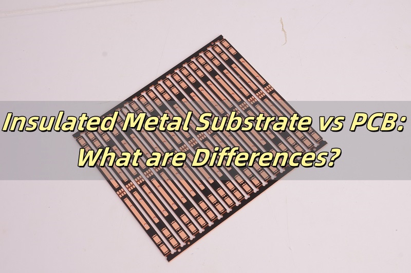
Are you always curious these questions about insulated metal substrate PCB:
What is insulated metal substrate? Does it the same as metal core PCB (MCPCB)?
What are the key differences between insulated metal substrate and standard PCB?
Can I use insulated metal substrate in my project? What’s its performance?
As a experienced PCB manufacturer, we can confident to say the insulated metal substrate (IMS) PCB is the same as mcpcb, there is no differences between them. But it is big differ from standard PCB. Actually, IMS PCB offer numerous benefits in high power or heat sensitive projects. In this blog we will introduce what is it, its performance and the differeces with FR4 PCB.
What is an Insulated Metal Substrate (IMS)?
An insulated metal substrate (IMS) is a type of metal core PCB designed for heat-intensive applications. Unlike traditional FR4 boards, IMS uses a metal base layer—usually aluminum or copper—covered with a thin dielectric insulation and a copper circuit layer on top.
The purpose of this design is simple: dissipate heat quickly while keeping the circuit stable. Aluminum IMS boards are most common, offering a balance of cost, strength, and thermal conductivity. Copper IMS is used where performance is critical, especially in high-current applications.
Key characteristics of IMS PCBs include:
High thermal conductivity to transfer heat away from components.
Strong mechanical stability compared to FR4.
Reliable performance in harsh environments.
For industries like LED lighting, automotive electronics, and power supplies, IMS PCBs have become a preferred choice.
What is IMS material for PCB?
The performance and cost of an insulated metal substrate PCB depend heavily on the choice of the base material. Different metals give different levels of thermal conductivity, mechanical strength, and pricing.
1. Copper IMS PCB
Copper has the best thermal conductivity among IMS options. It spreads heat rapidly and is highly stable under load. However, copper is expensive, so it is often reserved for high-power applications such as industrial converters or advanced automotive modules.
2. Aluminum IMS PCB
Aluminum is the most common choice for IMS PCBs. It strikes a balance between cost, weight, and thermal performance. With good heat dissipation and lower price than copper, it has become the preferred material in LED lighting and consumer automotive systems.
3. Iron IMS PCB
Iron-based substrates are rarely used. While they are strong, their lower thermal performance and processing challenges make them less attractive. In most cases, aluminum and copper dominate the IMS market.
What is a Traditional PCB?
A traditional PCB typically refers to a board made with FR4 substrate. FR-4 is a code for a fire-resistant material grade. It represents a material specification where the resin material must be able to extinguish itself when exposed to a burning condition. It is not a material name but a material grade. Most consumer electronics use FR4 PCBs because they are affordable and easy to manufacture.
The construction includes:
Fiberglass base (FR4) for insulation and strength.
Copper foil laminated on one or both sides.
Solder mask and silkscreen for protection and labeling.
FR4 PCBs work well in devices that do not generate extreme heat. They are versatile and suitable for phones, laptops, IoT devices, wearables, and household appliances.
What is the Difference Between Insulated Metal Substrate and PCB?
The key differences between ims pcb and traditional PCB is the base material, IMS pcb uses metal core as the base substrate while traditional PCB uses fiberglass epoxy. Due to the differences base materials used, their performance, price and applications are different accordingly. Here we listing a detailed table for your reference:
Feature
Traditional PCB (FR4)
Insulated Metal Substrate (IMS)
Base Material
Fiberglass epoxy (FR4)
Metal base (aluminum or copper)
Thermal Conductivity
Low (~0.3 W/mK)
High (2–10 W/mK dielectric + metal base can reach up to 400 W/mk)
Heat Management
Needs extra cooling (heat sinks, fans)
Built-in heat spreading through metal layer
Mechanical Strength
Rigid but less durable under vibration
Strong, resists shock and vibration
Flexibility
Can be rigid, flex, or rigid-flex
Mostly rigid only
Applications
Consumer electronics, IoT, computers
LED lighting, automotive, power modules
Cost
Low, highly economical for mass production
Higher, due to materials and processing
Why is IMS Better for Heat Dissipation Compared to PCB?
As we all know, heat is the biggest enemy of electronic components. If heat builds up, components degrade, solder joints crack, and lifespan shortens. Standard FR4 struggles to move heat away, leading to performance issues in high-power systems.
An IMS PCB solves this by using a metal base that acts like a built-in heat sink. The dielectric layer transfers heat from components directly to the metal, which spreads it out quickly. This keeps the board and devices cooler and improves the overall reliability.
This is why IMS PCBs are widely used in LED lighting, where heat directly impacts brightness and lifespan. Similarly, automotive systems like motor controllers and power converters use IMS to handle constant high currents.
Which Applications Do We Use IMS vs Standard PCB?
Each type of board has its own application areas.
IMS PCB applications
LED lighting systems
Automotive electronics (engine control units, sensors, chargers)
Power modules and converters
Industrial motor drives
Telecom base stations
FR4 PCB applications
Consumer electronics (phones, tablets, laptops)
IoT devices and smart wearables
Household appliances
Audio and multimedia systems
Office electronics
The decision depends on the heat level, power density, and cost balance.
Cost Differences Between IMS and PCB
IMS PCBs are more expensive than standard FR-4 boards due to their raw materials and processing steps. Aluminum-based IMS typically costs $0.12–$0.25 per cm², while FR-4 falls around $0.05–$0.10 per cm². Extra copper thickness, dielectric layers, and specialized drilling add further expense.
Yet, the higher upfront cost can translate into system savings. In LED lighting, automotive, and power modules, IMS often reduces the need for heat sinks or cooling parts. Studies show a 15–20% drop in overall system cost when FR-4 is replaced with IMS, thanks to better thermal control and longer product life.
Design Consideration of Insulated Metal Substrate PCB
Designing an Insulated Metal Substrate (IMS) PCB is more than just replacing FR4 with a metal base. The entire design strategy changes because thermal performance becomes the top priority. Several aspects need careful thought:
1. Dielectric Layer Thickness and Thermal Conductivity
The dielectric is the heart of an IMS PCB. Its job is to provide electrical insulation while transferring heat from the copper layer to the metal base.
Typical FR4 dielectric has thermal conductivity of 0.3–0.5 W/mK.
IMS dielectrics range from 2 to 10 W/mK, depending on material choice.
Thickness is usually 50–150 μm. Thinner layers transfer heat better but risk breakdown if not well controlled.
For normal LED boards, a 75 μm dielectric with 1-2 W/mK conductivity is often a balance between cost and reliability.
2. Copper Thickness and Trace Design
Current capacity is vital. Wider traces reduce resistance and heat buildup.
Standard FR4 PCBs often use 1 oz (35 μm) copper.
IMS boards commonly use 2–3 oz (70–105 μm) copper to carry higher currents.
IPC-2221 guidelines suggest that a 2 oz copper trace at 10 mm width can handle around 20–25 A continuously, which fits the demands of power devices.
3. Component Placement and Thermal Management
Hot components, such as MOSFETs, LEDs, or regulators, should be placed directly over areas where heat can spread into the metal base efficiently. Grouping high-power parts together without proper spacing often leads to localized hot spots.
Simulation tools (like ANSYS or thermal CAD software) are often used to map temperature rise. Data shows that placing components 5 mm apart can reduce local heat rise by 8–12°C compared to tightly packed layouts.
4. Board Thickness and Mechanical Strength
IMS boards are stiffer than FR4 due to the metal layer.
Common thickness: 0.8–3.2 mm.
For automotive PCBs exposed to vibration, a 1.6 mm aluminum base is typical for balancing rigidity and weight.
Designers should consider mounting holes and mechanical supports early to avoid stress cracking during assembly.
5. Surface Finishes and Soldering
Surface finishes like ENIG, ENEPIG, OSP or HASL are commonly applied. However, IMS boards undergo more thermal cycling during soldering, so ENIG is often preferred for reliability.
Factors Affect the Failure of Insulated Metal Substrate PCB
Even with proper design, IMS PCBs can fail if certain risks are not controlled. Failures usually stem from thermal, mechanical, or environmental stresses. Let’s examine the main causes, with supporting data:
1. Thermal Stress and Cycling
IMS PCBs are exposed to wide temperature swings, especially in LED lighting (-40°C to +120°C) or automotive control units (-55°C to +150°C). In additional, a thinner dielectric layer (<75 μm) is more likely to fail under repeated expansion and contraction. So, using high Tg dielectrics (Tg ≥ 170°C) and flexible solder materials reduces the chance of cracks.
2. Dielectric Breakdown
The dielectric layer separates copper circuitry from the conductive metal base. If the insulation fails, short circuits occur.
Standard IMS dielectric breakdown voltage: 2–6 kV/mm.
If the dielectric is too thin or contaminated during manufacturing, breakdown may occur earlier, especially in high-voltage power supplies.
3. Corrosion and Moisture Ingress
If the protective coating or solder mask is not properly applied, moisture, chemicals, or salts can corrode the copper traces or the aluminum base. There is no doubt that unprotected copper can corrode in under 72 hours in a salt spray environment (5% NaCl). Therefore, applying ENIG or OSP surface finishes greatly reduces corrosion risk.
4. Mechanical Stress and Vibration
IMS boards are less flexible than FR4, which means they can crack under excessive bending or vibration.
In automotive vibration testing (10–2,000 Hz sweep, 20 g), poor mounting caused delamination in 5–10% of samples after 50 hours.
Poor drilling, lamination errors, or uneven dielectric spreading can lead to early failures. For example:
Misaligned lamination can create voids, which increase heat resistance and raise local temperatures by 10–15°C.
Improper drilling of vias in IMS can leave burrs or microcracks, leading to premature electrical failure.
EBest Circuit (Best Technology) has more than 19 years in IMS PCB manufacturing. It cannot be denied that we had ever faced such problems and solved them finally, then we have much experiences to solve them and mature skills to avoid such defectives.
Insulated Metal Substrates Market
The insulated metal substrates market has grown rapidly with the demand for efficient heat management in electronics. Several sectors drive this expansion:
LED Lighting: As LEDs move into general lighting, street lamps, and automotive headlights, IMS boards remain essential for heat control.
Electric Vehicles (EVs): Motor controllers, inverters, and battery systems require durable IMS boards to handle high currents.
Industrial Power Systems: Power converters, motor drives, and renewable energy inverters are major adopters.
Telecom: Base stations and 5G equipment rely on IMS to stabilize performance under heavy workloads.
Market reports suggest steady growth in IMS adoption worldwide, especially in Asia-Pacific regions like China and South Korea, where LED and EV industries are booming. Aluminum IMS PCBs dominate due to cost efficiency, but copper IMS is growing in high-performance niches.
How to Choose Between IMS PCB and FR4 PCB?
The choice between IMS PCB and FR-4 PCB depends on performance demands, cost expectations, and application environment. If your design handles high power density or generates significant heat—such as in LED lighting, power converters, or automotive control units—IMS PCB is usually the better option. Its aluminum or copper base provides strong thermal conductivity, keeping component temperatures 20–30% lower than FR-4 under the same load.
FR-4 PCB, on the other hand, is more suitable for general-purpose electronics where heat generation is moderate. Devices like consumer gadgets, IoT sensors, and low-power communication modules often prioritize affordability and flexibility in design over extreme thermal performance. FR-4 also supports higher multilayer counts more easily than IMS, which is beneficial for complex circuits with dense routing.
So, in a word:
Choose FR4 PCB if your device is low-power, cost-sensitive, and not heat-intensive.
Choose IMS PCB if your design generates high heat, requires high reliability, or operates in harsh environments.
In practice, many manufacturers use both types in their product lines. Consumer electronics stay with FR4, while lighting and automotive turn to IMS.
FAQs
1. What materials are used in insulated metal substrates?
IMS PCBs usually use aluminum or copper as the base, with a dielectric insulation layer and copper foil.
2. Is IMS PCB more reliable than FR4 PCB?
Yes, especially in high-power or high-heat applications, IMS offers better thermal management and durability.
3. Can IMS replace all standard PCBs?
No, IMS is designed for specific heat-demanding uses. FR4 remains more cost-effective for everyday electronics.
4. Why are IMS PCBs used in LED lighting?
They transfer heat away quickly, improving brightness, efficiency, and lifespan of LEDs.
5. How expensive are IMS PCBs compared to normal PCBs?
IMS PCBs cost more due to metal materials and manufacturing, but they often save costs by reducing cooling needs.
About EBest Circuit (Best Technology) – Your Trust Insulated Metal Substrate PCB Supplier
EBest Circuit (Best Technology) is a turnkey PCB & PCBA manufacturer in China, we specialize in the design and manufacturing of high-quality PCBs, and we are confident that we can provide a tailored solution for your project. With our expertise and a broad range of materials, including SY, Rogers, Isola, KB, ceramic, metal core pcb, flex circuit and busbar copper pcb, etc, we offer flexibility and reliability for all your PCB designs.
We’ve made many PCBs for our customers, whether you need high-speed, high-frequency, or multi-layer PCBs, our experienced engineering team ensures reliable, cost-effective designs with excellent manufacturability. We’ve worked in this industry over 19 years, so we deeply know what our customers want, and make them into reality.
Our services include:
Customized PCB design based on your schematic and specifications
Free Design for manufacturability (DFM) to reduce production issues
Optimization for signal integrity, thermal management, and reliability
PCB layout and PCB design full turnkey service
Industry certifications we have:
ISO9001 (quality management system)
IATF16949 (for automotive device)
ISO13485 (for medical instrument)
AS9100D (aerospace applications)
In addition to our advanced PCB manufacturing capabilities, we also have a fully equipped SMT factory both in China & Vietnam. This facility is dedicated to providing our customers with professional PCB assembly services, including SMD soldering, component placement, and testing. This allows us to offer a complete solution, from PCB fabrication to final assembly, all under one roof. If you have PCB or IMS PCB manufacturing demands, welcome to contact us at sales@bestpcbs.com
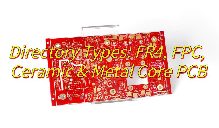
Would you like to know what types ofPCB directoryare? Let’s explore FR4, Flexible, ceramic and metal core PCB directories through this blog together.
At EBest Circuit (Best Technology), we can provide you service:
Competitive Price & Premium Quality– Maximize your budget with cost-effective PCBs that meet stringent quality standards.
24 Hours Rapid Prototyping– Accelerates product development cycles.
Free DFM (Design for Manufacturability) Support -Prevents manufacturing errors before production.
Full Turnkey Solution-handle PCB fabrication to assembly, saving vendor coordination time cost and production cost.
Feel free to contact us if you have any inquiry for FR4 PCB, FPC PCB, ceramic PCB and MCPCB: sales@bestpcbs.com.
What Is PCB Directory?
PCB Directory is a professional online service platform dedicated to the global printed circuit board (PCB) industry. It aggregates resources from manufacturers, assembly providers, and design service firms, facilitating efficient supplier matching through parameter-based categorization (e.g., material type, layer count, thickness) and geographic filters. The platform supports specialized requirements such as flexible PCB and ceramic PCB, streamlining supply chain collaboration in electronics manufacturing and serving as a critical industry information hub.
Have you experienced terrible thermal management problems?
Have you faced complexity in material selection and process?
Have you struggled with balancing quick prototyping and mass production?
Have you worried about the deficiency of the thermal management solution?
There are some optimal ways of dealing with the above issues.
Applying MCPCB thermal management solutions, which conduct heat from the circuit boards to the heat sinks.
Using thermally conductive dielectric materials to improve the thermal management capability of PCBs.
Optimizing quick prototype and fabrication. Employing a rapid prototype development process to shorten development cycles, reduce design changes, and manufacturing complexity via modular design.
Improving thermal management design. For example, using a thermal analysis tool to do thermal management design, and follow thermal management design rules to improve thermal management efficiency ultimately.
The design aim of thermally conductive PCB is conducting heat from components to keep stable circuit. Thermally conductive PCB is different from common PCB. It uses high thermal conductivity rate PCB material or metal core. Heat is conducted away through copper layers, thermally conductive vias, or the metal substrate. This design if of benefit to reduce temperature of chips and extend the lifespan of devices.
Is FR4 thermal conductivity?
FR4 thermal conductivity is low. Generally, it is only around 0.3 W/m·K. For low power device, FR4 is a good choice. However, in high power LED, automobile module or RF circuit, FR4 is not able to dissipate heat effectively. That is why designers move toward metal core boards, ceramics, or other high thermal conductivity PCB material. Many customers will meet some issues since they still use FR4 even in high heat loading situation. EBest Circuit (Best Technology) helps by suggesting better materials during the early design stage.
What’s the most high thermal conductivity PCB material?
Among all options, copper thermal conductivity is the highest at nearly 400 W/m·K. However, copper PCBs are heavy and costly. Aluminum is more cost efficient, and features good thermal conductivity, lighter weight. Ceramics such as aluminum nitride are also popular for their stability and high thermal conductivity PCB material values. It is good to know that engineers will select suitable materials based on costs, weights, and the applications.
What does thermally conductive tape do for metal core PCB manufacturer?
Thermally conductive tape is widely used with metal core PCB manufacturer solutions. It is able to bond components or heat sinks to the boards’ surface. This brings benefits of improving contact and reducing heat resistance. This small process gives boards the benefit of passing heat dissipation testing, and with the benefit of cost efficiency. It is crucial to note that many customers have delayed projects since their heat dissipation testing is failed. EBest Circuit (Best Technology) makes use well of thermally conductive tape, and you will enjoy benefits of short lead time and improved stability.
What is the relation: thermally conductive PCB, PCB thermal resistance?
The link between thermally conductive PCB and PCB thermal resistance is direct. PCB thermal resistance refers to the transferring efficiency of heat between layers. The lower PCB thermal resistance, the sooner heat dissipation. Thermally conductive PCB can reduce hot spots, which promotes the benefits of stability, and the higher power density. Hence, during prototyping, PCB thermal resistance parameter is key element that customers pay highly attention to.
How to use a PCB thermal conductivity calculator when selecting thermal conductivity PCB material?
A PCB thermal conductivity calculator helps predict how heat flows through materials. Input thickness, copper area, material types and other parameters by engineers, then the tools will present the result. In this way, the mistakes will be reduced. However, it is common to know that customers don’t have time to do the double checking. By using calculators, EBest Circuit (Best Technology)’s engineers help save time and reduce risk by providing guidance early.
Why is a thermally conductive gap filler important for high thermal conductivity PCB material?
Thermally conductive gap filler bridges air gaps between parts and board. Air will isolate the heat transferring. But gap filler is able to conduct heat efficiently. For high thermal conductivity PCB material, the gap filler keeps the surface contact smooth and efficient. Otherwise, even the copper or ceramic boards, the effect will be largely lessened. This is significant for power electronics and LEDs particularly.
What are the applications of thermally conductive PCB?
The applications include LED lighting, electrical automobile, 5G equipment, satellite modules and the industrial drives. In these applications, heat is the most terrible enemy of performance. Thermally conductive PCB manages heat in the circumstance that it does not increase large heat sinks. Since it reduces the weight, which is useful and essential to the aerospace and automobile. And customers hope to get prototypes quickly in general. EBest Circuit (Best Technology) can meet this kind of demands via flexible prototyping service.
Where to get quick thermally conductive PCB from prototypes?
It is a bottleneck problem for finding a suitable supplier. Since various company has the issue of seriously delayed delivery time or the hopeless quality control. EBest Circuit (Best Technology) provides a faster path. We promise the traceability via applying MES system. Besides, we offer a full quality guarantee. Our factory is fully compatible with ISO 9001, ISO 13485, IATF 16949, AS9100D, UL, REACH, and RoHS standards. Our company is to fully dedicate ourselves to do DFM analysis, review the thermal design problem during prototyping, so that customers get not only our rapid prototypes but also our professional and workable solutions. In this way, we can accelerate the market entry time and reduce the rework costs in the meanwhile.
In a nutshell, for the electronic products, heat dissipation is indispensable. Every process decides the final performance, from material selection to the prototype delivery. We know some customers often suffers the headaches for the overheating or long delivery time. EBest Circuit (Best Technology) solves customers’ headaches through quick thermally conductive PCB prototyping, professional technical support, and strict quality management. For those seeking a trusted thermally conductive PCB partner, EBest Circuit (Best Technology) is ready to help. A warm welcome to contact us via sales@bestpcbs.com for our highly professional supports.
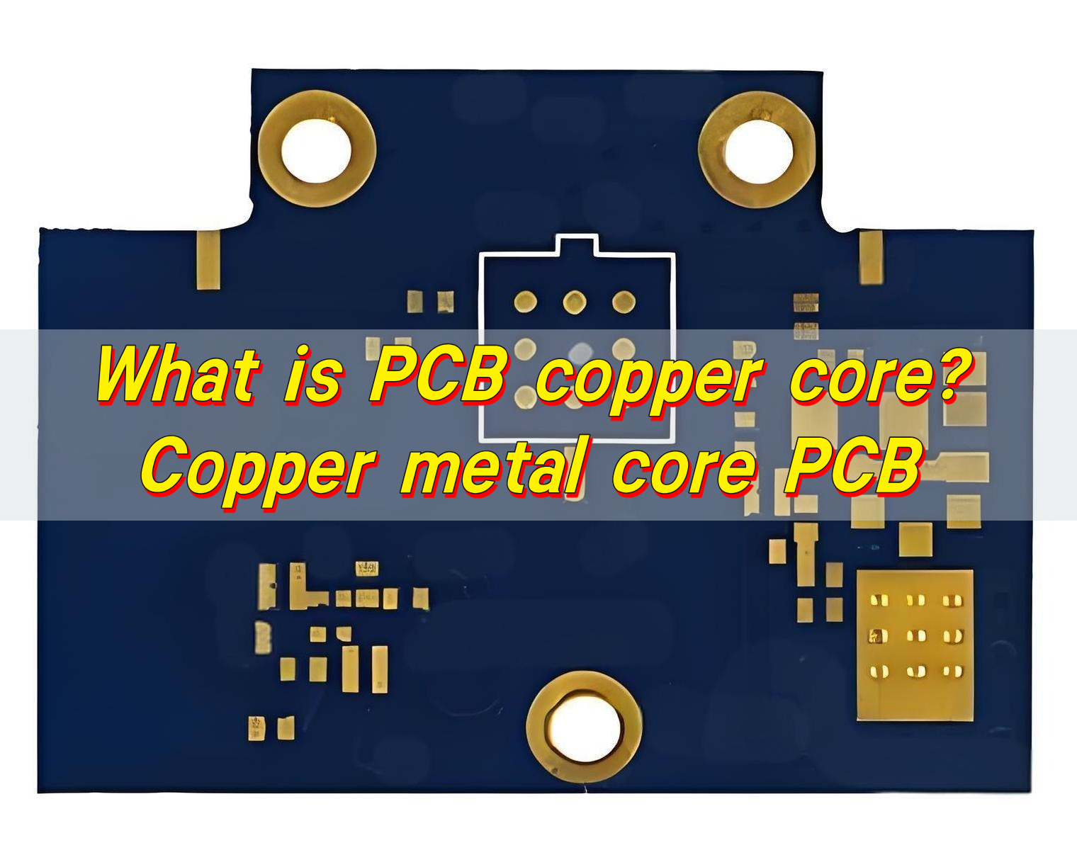
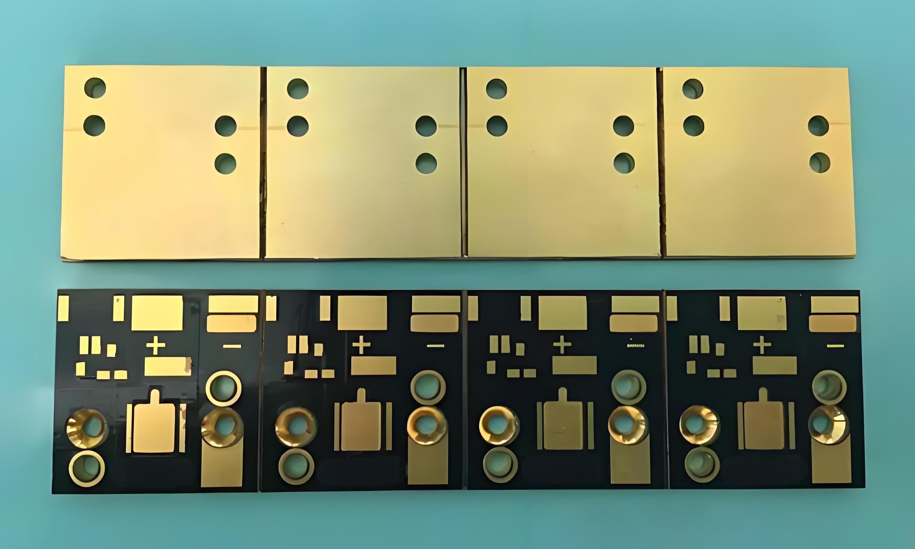
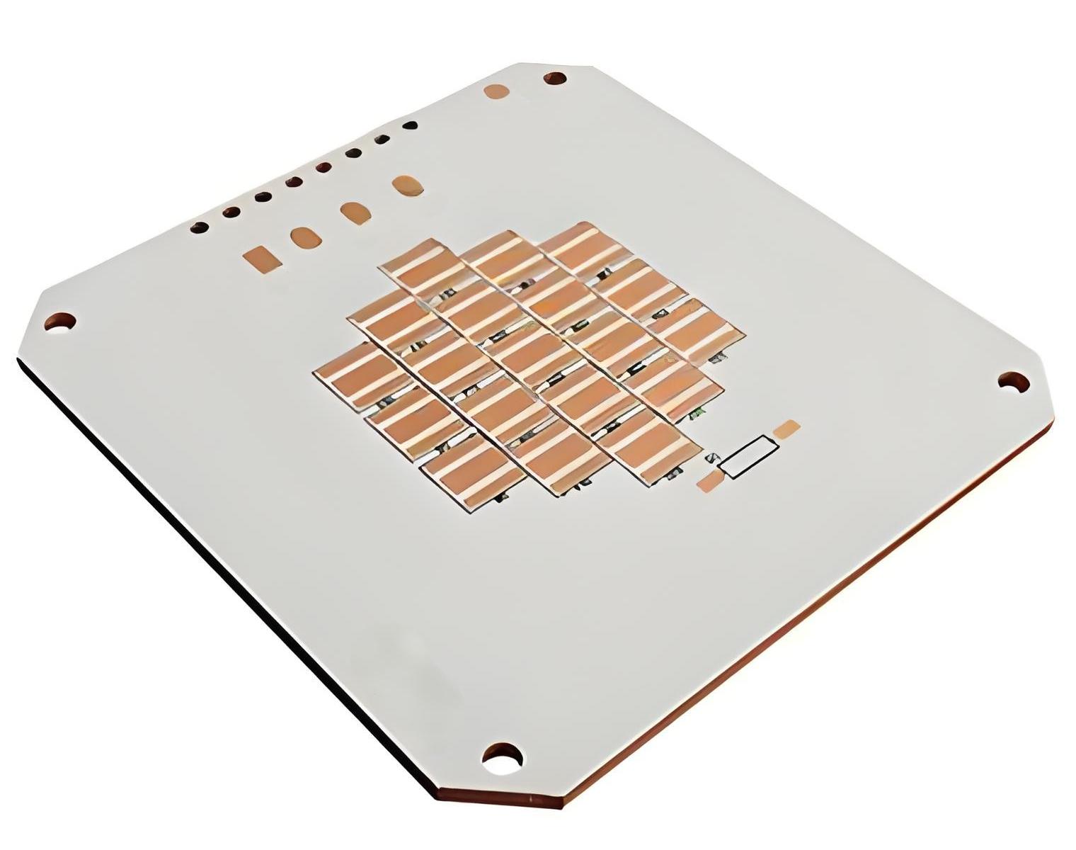
PCB copper core stands out among other PCB types due to its high thermal and power capabilities. These boards are designed to operate in harsh environments, offering exceptional durability and reliability.
Maybe you have these worries and concerns:
Can the copper thickness and thermal conductivity of copper core PCBs be precisely tailored to meet specific requirements?
How can I avoid delamination and oxidation of the copper core? How can I resolve issues if they arise?
Can I guarantee sample or batch delivery?
Are there any industry examples? Can I receive a 24-hour response to after-sales technical questions?
BEST Technology can solve your problem:
We support custom copper thicknesses from 0.5-10 ounces, and precisely match power requirements through zoned thermal design.
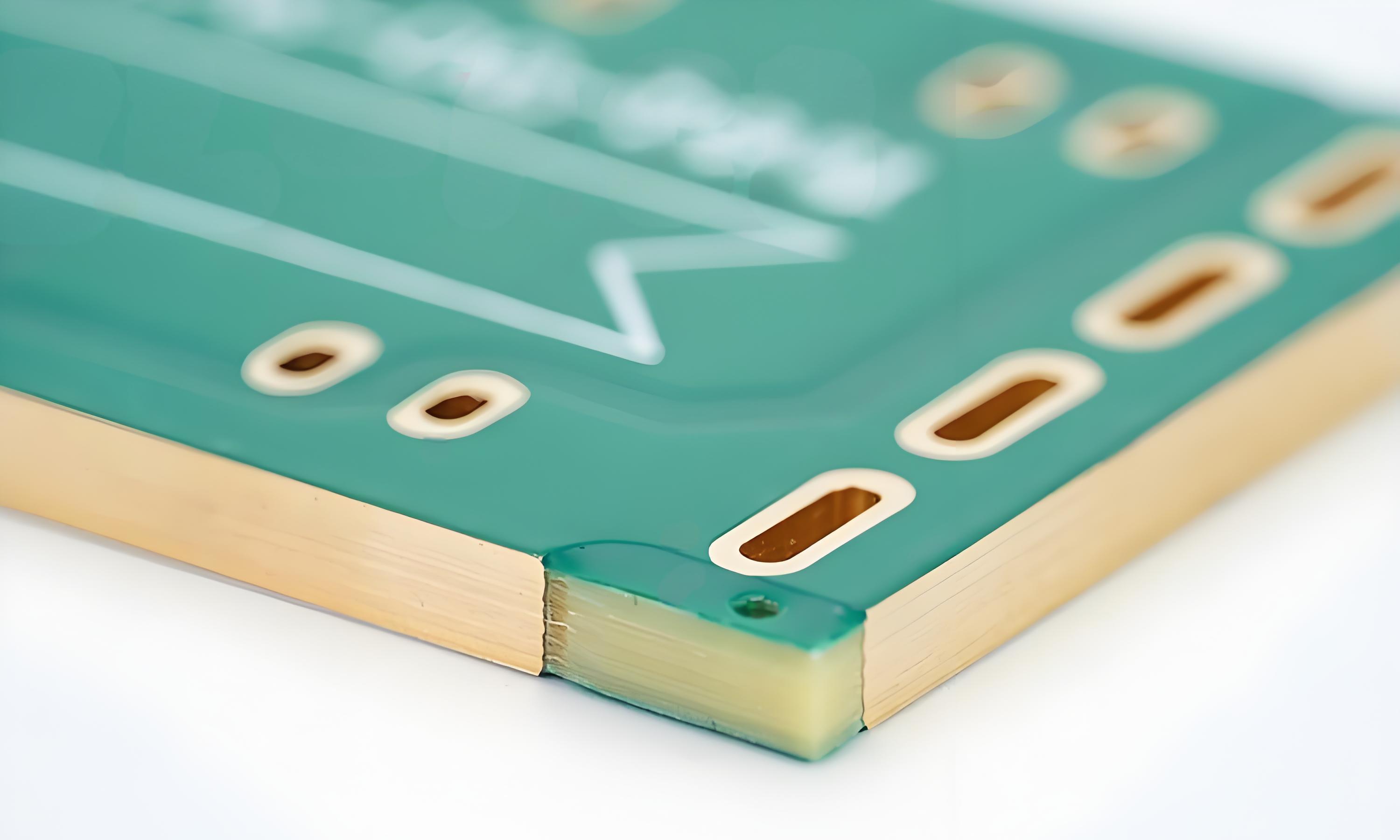
We utilize vacuum lamination and an anti-oxidation coating (such as OSP or immersion gold) to ensure interlayer bonding strength ≥1.8N/mm² and pass 1000 cycles of -40°C to 125°C temperature cycling testing without delamination. We offer free rework or replacement for delamination and oxidation issues within the warranty period, with a 48-hour response and solution.
This material has been widely used in new energy vehicle BMS systems (10oz copper thickness), industrial inverters (8oz multilayer boards), and 5G base station power modules (6oz copper core). We provide 24-hour remote support to ensure rapid resolution of technical issues.
What is a copper core PCB?
Copper core PCB is a type of printed circuit board with a solid copper layer at its core. Unlike traditional PCBs, where copper is only part of the circuit paths, the core itself is copper. This provides superior thermal conductivity, allowing heat to be efficiently managed in high-power applications.
The copper core acts as a heat spreader. It moves heat away from sensitive components. This prevents overheating and maintains long-term performance. These boards are widely used in LED lighting, automotive electronics, industrial equipment, and power electronics.
Using a copper core also improves the mechanical stability of the board. Components remain securely in place even under heat stress. The copper’s high conductivity ensures that both electrical performance and heat dissipation are optimal.
Why Use a Copper Core PCB?
Modern electronics often produce significant heat, which can reduce efficiency and shorten the life of components. Copper core PCBs solve this problem efficiently.
Here’s why they are used:
High thermal conductivity: Copper efficiently transfers heat away from components, keeping devices cooler.
Durability: They withstand thermal cycling better than standard FR4 boards.
Compact design: Designers can place components closer together without worrying about overheating.
Energy efficiency: Reduced heat buildup enhances performance and reduces energy loss.
In short, using a copper core PCB increases reliability, extends device life, and supports high-power applications where traditional PCBs would fail.
How is a Copper Metal Core PCB Made?
The manufacturing of a copper metal core PCB differs from standard PCB production. It requires precision and advanced techniques.
Step-by-step process:
Copper sheet selection: High-purity copper sheets are chosen for the core. Purity ensures consistent thermal conductivity.
Insulation layer application: An insulating dielectric layer is added to separate the copper core from the circuit traces.
Copper layering: Copper foil is laminated on both sides of the dielectric layer. This creates the circuit paths.
Etching: The unwanted copper is chemically removed to form the desired circuit design.
Surface finish: Methods like HASL, ENIG, or immersion silver are applied to protect the copper and improve solderability.
Testing and inspection: Each board is rigorously tested for electrical continuity, thermal performance, and mechanical stability.
This process ensures that copper core PCBs perform well under high thermal and electrical stress.
Do PCBs Have Copper?
Yes, copper is a standard material in all PCBs. It forms the conductive pathways that carry electricity. Standard FR4 PCBs use copper only in traces and pads.
Copper core PCBs are different. The copper is in the core, not just the circuit layers. This gives them superior heat conduction. Components stay cooler, even under heavy loads.
Copper’s excellent electrical and thermal conductivity ensures stable performance. Devices work reliably for years without overheating.
What Type of Copper is Used in PCB?
The type of copper affects both thermal and electrical performance. In copper core PCBs, BEST Technology typically use:
High-purity electrolytic copper: Provides consistent conductivity and low resistance.
Oxygen-free copper (OFC): Reduces oxidation and ensures long-term stability.
Rolled annealed copper: Offers flexibility and mechanical strength for assembly.
Choosing the right copper type ensures high thermal conductivity, strong mechanical support, and stable electrical performance. This is especially important in LEDs, automotive electronics, and industrial equipment.
The Types of Copper-Based PCB
Copper-based PCBs can vary depending on the application. The main types include:
Single-layer copper core PCB: Features one conductive layer. Often used in simple LED modules or low-power devices.
Double-layer copper core PCB: Has copper on both sides. This design supports more complex routing while maintaining heat management.
Multilayer copper core PCB: Includes multiple circuit layers with a central copper core. Ideal for high-power, dense electronics.
Flexible copper core PCB: Thin copper sheets with flexible substrates allow heat dissipation and adaptable design.
Each type is tailored for specific needs. LEDs often use single or double-layer boards. Industrial and automotive applications prefer multilayer copper core PCBs.
Is Copper Core or Aluminum Core Better?
Both copper and aluminum core PCBs are designed to manage heat efficiently. However, copper offers several advantages.
Advantages of copper core:
Higher thermal conductivity.
Better electrical performance.
Greater long-term reliability.
Advantages of aluminum core:
Lower cost.
Lightweight construction.
Suitable for moderate heat applications.
While aluminum cores are cost-effective, copper core PCBs outperform them in thermal management, reliability, and longevity. This makes copper the preferred choice for high-power and high-reliability electronics.
Copper Core vs Aluminum Core – Thermal Conductivity
Thermal conductivity determines how efficiently a material transfers heat. This is critical in electronics design.
Copper core PCB: Typically 300–400 W/m·K.
Aluminum core PCB: Typically 1-30 W/m·K.
Copper conducts heat several times faster than aluminum. This keeps components cooler and prevents hotspots. Electronics run efficiently and last longer when heat is managed properly.
Conclusion:
PCB copper core ensures excellent thermal conductivity. Components stay cool, even under high power or prolonged use. Copper core PCBs are durable, reliable, and suitable for compact designs. Compared to aluminum, they provide higher conductivity, better performance, and longer lifespan.
These boards are widely used in LED lighting, automotive electronics, industrial equipment, and power modules. Choosing a copper core PCB improves efficiency, safety, and product reliability.
BYD automotive LED aluminum substrate is a specially designed metal-core printed circuit board used in automotive LED lighting, providing excellent heat dissipation, mechanical stability, and reliable electrical performance. In this blog, you will find some significant information about the definition, features, types, materials, functions, working principle, manufacturing process, main applications, and cases about BYD automotive LED aluminum substrate.
Have you ever complained about these headaches before?
Troublesome thermal dissipation problem?
Worrying about deficits of manufacturing and design?
Bothersome material and process problem?
Difficult reliability and lifespan problem?
Here are the efficient solutions EBest Circuit (Best Technology) provides to solve the above issues for your reference.
Adjust heat dissipation design: EBest Circuit (Best Technology) makes use of the high conductivity rate of the aluminum substrate and applies heat dissipation structure, such as heat sinks, to boost efficiency.
Employ strict manufacturing and quality control: We adopt cutting-edge manufacturing processes to ensure the stable performance of the products. Besides, we strictly control material selection and process parameters to ensure every PCB is fully compatible with the standards.
Enhance inspection and verification: We exploit innovative inspection equipment and methods to ensure the stable PCB performance.
Boost the customer support and cooperation: We present quick prototype design, small batch manufacturing, turnkey assembly, quick delivery and other services to meet customers’ requirements.
EBest Circuit (Best Technology) has precious experience to provide sensible, tailored solutions of BYD automotive LED aluminum substrate. Our metal core PCBs and services include prototype to PCBA. If you need high quality and reliable aluminum LED board substrate, a warm welcome to contact us at sales@bestpcbs.com.
What is BYD Automotive LED Aluminum Substrate?
In short, it is a metal-based printed circuit board used in BYD vehicle lighting. It adopts an aluminum substrate to boost heat dissipation and mechanical strength. And the copper layer is isolated via the insulated layer, to ensure the LED current is well distributed. The structure supports high lumen density, meanwhile, keeps junction temperature low, ensuring the long-term stability of the brightness and colors.
In comparison with traditional FR4, the aluminum substrate conducts heat faster, which allows LEDs to be placed in high density for a compact space. Besides, the metal base improves rigidity and vibration tolerance. It adapts to the heat shock of the vehicle and the vibration of roads during driving.
What are the features of BYD Automotive LED Aluminum Substrate?
Excellent thermal dissipation: Low heat resistance keeps low LED junction temperature, stable lumen and color, and long lifespan.
Safe electricity: A highly insulated layer ensures electrical pressure loading capability, and the single-sided layouts meet the distance and the creepage requirements.
Mechanical strength: aluminum substrate features of warp resistance and shock resistance, which are beneficial for mounting of lenses and brackets.
Stable manufacturing: Clean copper layer, good solder paste, and finally, the low rework rate.
Cost efficiency: It reduces layers and processes for single-layer layouts, and the tools are simple; finally, the yield rate is high.
What are the Types of BYD Automotive LED Aluminum Substrate?
Here are the types of BYD automotive LED aluminum substrates.
Single-sided aluminum substrate: The most common choice for lamps and DRL strips.
Boosted insulated IMS: The Insulated layer thickness or the breakdown pressure will be higher.
High-thermal IMS: Dielectric engineered for lower thermal resistance, which is good for compact spaces and high flux.
Hybrid boards: The LED area uses aluminum, and the control circuit area uses FR4.
Rigid-flex circuit boards: Adopt an aluminum substrate for segments, connected with Flex cables, suitable for bended lighting strips.
What materials are used in an LED single-sided aluminum substrate?
First, the aluminum base in 1.0–2.0 mm thickness with 5052 or 1060 grades is often used.
Second, the thermal conductivity insulated layer is 75–150µm.
Third, copper foil in 35–105 µm.
The solder paste protective layer and white surface coating will improve the optical gain.
Finally, it is worth mentioning that the surface treatments are OSP or ENIG.
It is helpful to note that it needs to consider the thermal conductivity, insulation, and cost when doing the material selection.
What are the functions of aluminum substrate backed single layers boards for the LED lighting industry?
The main functions include thermal dissipation, electrical conductivity, and the mechanical structure support (which includes lenses and the bracket).
Thermal dissipation: It is through the aluminum base and aluminum layer to realize fast thermal transmission.
Electricity conductivity: The copper foil circuit is used in current transmission.
Mechanical support: It provides a rigid structure to LED modules, lenses, and the heat sinks, particularly for automobile applications.
In an automobile, these functions take center stage. Single-layer boards are a practical foundation in applications.
How does an aluminum LED board substrate work in BYD automotive lighting?
It is important to understand the core mechanism that enhances thermal dissipation efficiency and operational stability.
First, there is the separated structure design, which is an aluminum core, an insulated layer, and a copper foil circuit layer.
Aluminum core, such as 6061 aluminum alloy, offers mechanical support, which high thermal conductivity is up to 200–235W/m·K. It is beneficial to conduct heat away where LED chips are generated.
Besides, it is through an insulation layer to ensure the electrical isolation, meanwhile to keep the heat conductivity, with a heat conductivity coefficient of 1–3W/m·K.
Finally, the copper foil circuit layer is through etching to form the circuit, which connects the LED chips and the drive circuit.
Optimizing the thermal dissipation route is essential.
Heat passes layer by layer: LED chips → insulation layer → aluminum substrate → heat sinks.
Compared to traditional FR4, heat resistance is reduced by over 50%.
Automobile-grade strengthened designs are also notable.
The structure resists corrosion in moisture and salt spray environments and withstands vibration, with the aluminum core providing a 1.0 mm rigid layer.
Finally, it is worthy to note of the integration benefits.
The single-layer deisgn simplifies the assembly, and reduce the material of the heat sinks and interface, reducing weight and costs.
This design helps to maintain the lifespan over 50,000 hours even if in high temperature, high moisture situations.
What is the manufacturing process of BYD Automotive LED Aluminum Substrate?
1. Data review: It is significant to check the stackup and IPC standards.
2. Material prep: Aluminum base cutting and deburring. Copper-laminate and dielectric selection based on thermal and voltage targets.
3. The dry film explosion: Transferring copper circuit pattern.
4. Etching: Controlling the line width precision.
5. Drilling: Including mounting holes and optical alignment holes.
7. Coating: Proceed Solder paste and white coating
8. V-cut/route: Panels prepared for smooth depaneling at the SMT line.
9. Reliability inspection: pressure resistance, heat shock, solderability, and the smooth level.
10. QA: Finalize the QA and packing
What are the main applications of aluminum LED board substrate in BYD LED lighting?
The core applications are as follows:
Headlamps and DRLs: High flux LED arrays with precise optics. It avoids the lumen depreciation since the high heat conductivity of the aluminum substrate conducts the LED chips’ heat quickly.
Fog lamps: Compact housings with strong heat paths. Good for wet and cold cycles.
Power and control modules: For example, the electrical adjust device or controlling device is for power transferring, such as a DC / AC inverter. Aluminum has a high current loading capability up to 4500V pressure resistance, and has low heat resistance, which largely improves the reliability.
The Taillights/Interior lighting: It meets the thinner and lighter-weight needs via the high density assembly of the SMT process.
It is important to note that the heat conductivity rate of the aluminum substrate boards is of over 6.7 times that of the FR4. Hence, it will be a good fit for high-power LED lighting.
Case about BYD Automotive LED Aluminum Substrate
Here is a condensed case from a recent platform lamp refresh for our customer.
We proposed a single-sided aluminum substrate with a high-thermal dielectric. A thin thermal pad bridged the back to the cast housing. Junction temperature dropped by 16–22 °C in the worst case.
It has the key wins that it has less heat at the LED. Cleaner color over life. Higher yield at SMT. And no tooling changes. That is one of the true solutions of a well-built aluminum LED board. Here are some of our parameters and corresponding PCB pictures for your reference.
Layer: 2 Layer (Single Sided Aluminum PCB)
Material: FR-4+AL base pressed, 1.6 mm, 2 oz/2 oz, 100 μm insulated layer, 3 W/(m·K)
Workmanship: FR-4+AL base pressed, CNC routing, aluminum back groove
Application: Automotive LED lighting, industrial control
Why choose EBest Circuit (Best Technology) for aluminum substrate LED manufacturing?
EBest Circuit (Best Technology) focuses on the high quality aluminum substrate LED manufacturing and the assembly service to a highly competitive market.
Quick Quote: Our engineers reply the inquiry with 4 hours. We will confirm the stackup and process, and will give the rational solution with the specific quote.
Quick delivery time: We will evaluate the delivery time in advance and will update the manufacturing schedule. We promise 2 – 3 weeks delivery time no matter how complicated the boards are.
Optimized design: Our engineers will improve insulation, aluminum material, and the thermal dissipation design.
Comprehensive quality system: Our factory is full compatible with ISO 9001, ISO 13485, IATF 16949, AS9100D, UL, REACH, and RoHS standards. We will meet your requirements of automobile, medical, and aerospace grade requirement. You can enjoy our full technical support.
In conclusion, BYD automotive LED aluminum substrate features reliable heat dissipation and optical stability, which could meet the stable lighting and the lasting brightness requirement of BYD automobile. If you would like to find a reliable manufacturer to tackle the pain points of material procurement, engineering, lead time, or LED PCB performance, just feel free to get in touch with us at sales@bestpcbs.com, and we will ensure your project runs smoothly.
What isaluminum PCB etching? Let’s explore its principle, application, etching process, technical parameter, common problems and solutions, differences between copper PCB etching.
Are you troubled with these problems?
Why does aluminum PCB etching yield stay stuck at 80%?
How to eliminate copper burrs after etching?
Is there a permanent fix for thin aluminum warping?
EBest Circuit (Best Technology) can provide service and solution:
Aluminum PCB etchingis a manufacturing process that removes excess copper foil from aluminum based circuit boards using chemical solutions (e.g., acidic copper chloride), forming desired conductive traces while maintaining structural integrity. Unlike traditional FR4 etching, aluminum substrate etching requires strict control of temperature, pressure, and etch rate to minimize side erosion (≤15%) and ensure line width/space accuracy (≥0.2mm), especially for high-power applications like motor control boards.
19 Years of Aluminum Substrate R&D Expertise: Specialized in high-power aluminum PCB development since 2006, with over 500 global client projects delivered across industrial lighting, automotive electronics, and communication equipment.
Dual-Certification Quality System: ISO 9001/IATF 16949 dual certification, compliant with medical (ISO 13485) and automotive standards. 100% AOI inspection ensures zero tolerance for solder bridges, misalignment, or copper residues.
Industry-Leading Etching Precision: Utilizes pulsating etching process (3-second spray / 0.5-second pause) with 5-10% glycerol additive, achieving ≤15% side etch rate and ±0.02mm line width accuracy, supporting 0.15mm ultra-fine circuit processing.
Thermal Management Innovation: Proprietary heat dissipation design reduces device operating temperature by 30%, paired with 3W/m·K high-thermal-conductivity aluminum substrates for stable performance in high-temperature environments.
24-Hour Rapid Prototyping: Direct import of Altium/PADS design files, coupled with in-house etching lines, enables 24-hour prototype delivery and 48-hour shipment, accelerating time-to-market.
Free DFM Design Optimization: Engineering team pre-reviews thermal via layouts and trace spacing, proactively mitigating etching defects and reducing rework costs by over 40%, especially for complex multilayer designs.
Eco-Friendly & Cost-Effective Solutions: Lead-free etching processes and 25% recycled aluminum content meet RoHS/REACH standards while offering budget-friendly options for mass production, balancing performance and affordability.
Welcome to contact us if you have any inquiry for aluminum base PCB: sales@bestpcbs.com.
LED double-sided aluminum substrate is a high thermal conductivity circuit board with copper wiring on both sides of the aluminum substrate. LEDs are soldered on one side and drive or control circuits are carried on the other side. The aluminum core in the middle dissipates heat quickly, allowing high-power lamp beads to operate stably in a smaller space. It has been widely used in automotive headlights, street lights and high-density backlight modules.
Are you curious about EBest Circuit (Best Technology)’s LED double-sided aluminum substrate?
Will double-sided wiring lead to short circuits or signal distortion due to inaccurate interconnections?
Is heat dissipation balanced on both sides, preventing localized overheating that could affect the life of the lamp?
Will the copper foil easily peel off after repeated soldering?
Does the cost of double-sided processing justify the performance improvement?
EBest Circuit (Best Technology)’s LED double-sided aluminum substrate can answer these questions.
Using high-precision drilling and alignment processes, interconnect holes are precisely positioned, providing reliable insulation and preventing short circuits or signal issues.
The double-sided aluminum base design, with its symmetrical heat dissipation path, ensures even heat conduction, reduces localized overheating, and extends the life of the lamp.
The copper foil and aluminum base are tightly bonded through a high-temperature pressing process, resistant to soldering heat shock and maintaining stable adhesion after repeated soldering.
The double-sided design increases circuit density and heat dissipation efficiency. Process costs are optimized through large-scale production, and the performance improvements far outweigh the cost increases.
What is double sided aluminum PCB?
Double-sided aluminum PCB is a printed circuit board with aluminum as its base material, featuring copper layers on both sides. It includes an insulating dielectric layer between the copper and aluminum base. This design enables routing on both sides, unlike single-sided boards that only allow traces on one side.
Because aluminum offers excellent heat dissipation, these boards are widely used in high-power LED lighting. They prevent overheating, which can damage LEDs or reduce their lifespan.
With two conductive layers, double-sided boards also allow more complex circuits, making them ideal for advanced LED assemblies.
Types of double-sided aluminum PCB
Double-sided aluminum PCBs come in different forms, depending on application needs. The most common types include:
Standard Double-Sided Aluminum PCB: These have two copper layers and a dielectric layer between the aluminum base. They are simple yet effective for medium-power applications.
Hybrid Double-Sided PCB: This type of substrate combines the benefits of two different materials, such as aluminum and ceramic, to provide improved thermal conductivity and electrical performance.
Flexible Double-Sided PCB: This type of substrate is made of a flexible material and has a layer of aluminum on both sides. It is commonly used in applications where flexibility is required, such as in wearable electronics.
High-frequency double-sided aluminum PCB: This type of substrate is designed for high-frequency applications and has a low dielectric constant, which helps to reduce signal loss.
Each type serves a specific purpose. Choosing the right one depends on thermal requirements, circuit complexity, and mechanical needs.
How does a double-sided aluminum PCB differ from a single-sided one?
Single-sided aluminum PCB has one copper layer for circuit routing, limiting its complexity. A double-sided board, on the other hand, has two copper layers, allowing for denser component placement and more advanced designs.
Another major difference is thermal management. Both provide excellent heat dissipation thanks to the aluminum base, but double-sided boards handle higher power loads better. This is crucial for high-brightness LED systems where heat can build up quickly.
Lastly, cost and assembly differ. Double-sided boards may cost slightly more.
What materials are used in LED double-sided aluminum substrates?
LED Lighting Systems: Indoor, outdoor, and industrial lighting where thermal management is critical.
Automotive Lighting: Headlights, tail lamps, and dashboard lighting.
Consumer Electronics: Devices that require compact yet heat-resistant boards.
Medical Devices: Surgical lights and diagnostic equipment that must stay cool for safety.
Power Electronics: High-power converters and power supplies where heat is a major concern.
The ability to handle high power and maintain stability under heat makes these substrates essential for advanced applications.
How is a double-sided aluminum PCB manufactured?
The manufacturing process involves several precise steps:
Aluminum Base Preparation: The base is cleaned and treated to improve adhesion.
Dielectric Layer Application: A thermally conductive but electrically insulating layer is added.
Copper Foil Lamination: Copper is laminated on both sides under heat and pressure.
Circuit Patterning: Copper layers are etched to create circuit paths.
Drilling and Plating: Holes are drilled and plated to connect layers.
Surface Finish: ENIG, HASL, or other finishes are applied for better solderability.
Solder Mask and Silkscreen: Applied for protection and labeling.
Testing: Each board undergoes electrical and thermal testing to ensure quality.
Precision is key to achieving tight tolerances and long-lasting performance.
What are the applications of double-sided aluminum PCB?
These boards power a wide range of industries:
LED Lighting: Streetlights, floodlights, and smart lighting solutions.
Displays and Signage: High-brightness displays that run for long hours.
Telecommunication Equipment: Devices where heat control is essential for reliability.
Aerospace and Defense: Applications requiring extreme durability and stability.
Renewable Energy: Solar inverters and power control systems that demand high thermal performance.
Wherever heat and reliability matter, double-sided aluminum PCBs are the go-to solution.
Conclusion:
Double-sided aluminum substrates for LEDs are able to handle high power, dissipate heat efficiently, and support compact designs without compromising performance. Their advantages over FR4 make them the best choice for demanding applications.
If you need custom LED aluminum substrates for your projects, EBest Circuit (Best Technology) is here to help. We provide premium-quality aluminum PCBs, strict quality control, and fast delivery. Contact us today at sales@bestpcbs.com