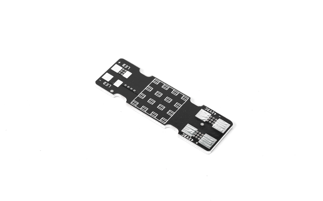
What is 1 oz copper PCB? This guide covers specifications, manufacturing, and selection criteria for optimal circuit performance.
- 1 oz copper foil is too thin? Worried about insufficient current carrying capacity and burning the circuit?
- Can the thickness tolerance of 1 oz copper PCB be stable during mass production?
- The budget is limited, but the poor heat dissipation of ordinary PCB affects the lifespan?
EBest Circuit (Best Technology) Can Provide:
- Precise current carrying design: 1 oz copper foil + optimized line width, meeting 20A+ current (IPC-2152 standard verification).
- ±5μm thickness control: laser thickness gauge real-time calibration to ensure batch consistency.
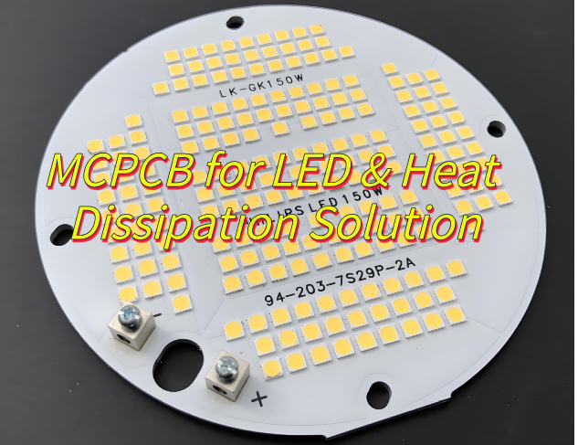
- Cost-effective heat dissipation solution: metal base/FR4 hybrid structure, thermal resistance reduced by 40%.
Welcome to contact us if you have any request for copper PCB board: sales@bestpcbs.com.
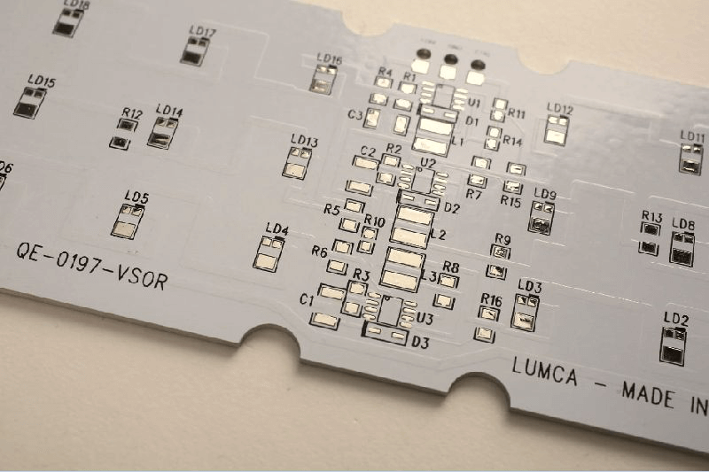
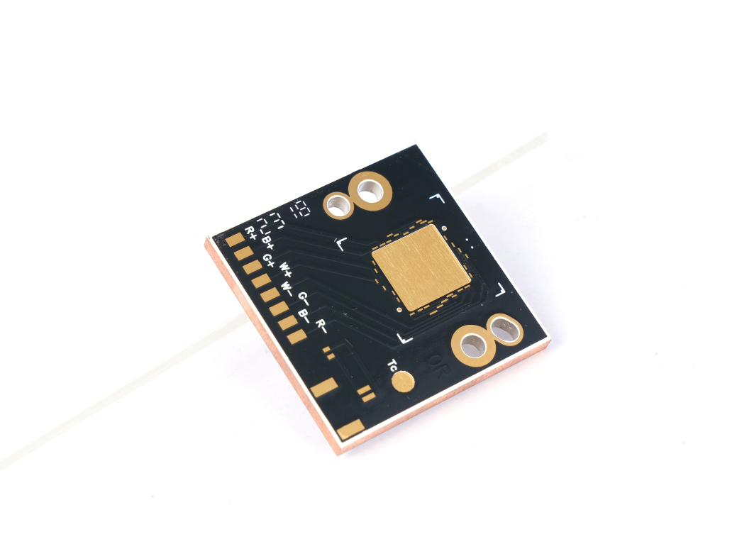
What Is A 1 oz Copper PCB?
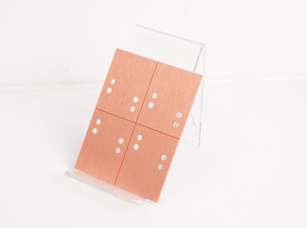
A 1 oz copper PCB utilizes a copper layer thickness defined by the historical unit “ounce per square foot” (oz/ft²), where 1 ounce of copper is uniformly spread over one square foot of surface area. This results in a physical thickness of approximately 35 micrometers (µm) or 0.0348 millimeters. This standardized measurement balances electrical conductivity, manufacturability, and cost-effectiveness for a wide range of electronic applications.
It serves as the fundamental benchmark for conductivity and current-carrying capacity in most printed circuit boards across consumer electronics, industrial controls, and communication devices. Designers carefully correlate trace widths with this 35µm copper thickness to ensure adequate current flow without excessive voltage drop or overheating. While thicker copper layers exist for high-power applications demanding greater ampacity or thermal dissipation, the 1 ounce copper specification remains prevalent due to its optimal performance in standard circuits and efficient fabrication processes.

What Is the Thickness of 1 oz Copper PCB?
The thickness of a 1 oz copper PCB is defined by the industry-standard weight-to-area measurement. Specifically, 1 ounce (oz) of copper uniformly distributed over one square foot (ft²) area results in a physical thickness of approximately 35 micrometers (µm) or 0.035 millimeters (mm). This equivalently translates to about 1.4 mils (thousandths of an inch) in imperial units.
What Is the Height of 1 oz Copper PCB?
The height (thickness) of 1 oz copper on a printed circuit board (PCB) measures 35 micrometers (µm), equivalently 0.035 millimeters (mm) or 1.4 mils (thousandths of an inch). This standard thickness results from the industry practice where one ounce of copper is uniformly distributed over one square foot of surface area. The calculation accounts for copper density at approximately 8.92 g/cm³ to achieve consistent thickness values that ensure manufacturing reliability and electrical performance.
What Is the Current Capacity of 1 oz PCB?
The current-carrying capacity of 1 oz copper PCB traces depends on width and temperature rise. A standard 10mm (0.4″) wide 1 oz (35µm) trace can safely carry about 5A with a 10°C temperature rise, or up to 8A with a 20°C rise. For precise calculations, use the IPC-2152 standard or online PCB trace width calculators that account for copper thickness, ambient temperature, and desired temperature rise.
Differences Between 1 oz vs 2 oz Copper PCB
| Aspect | 1 oz Copper PCB | 2 oz Copper PCB |
| Thickness | 35 micrometers (µm) or 1.4 mils | 70 micrometers (µm) or 2.8 mils |
| Current Carrying Capacity | Lower; typically <5A for standard designs, e.g., ~4.6A at 1mm line width with 10°C temperature rise | Higher; ~40% increase vs. 1 oz, suitable for >5A currents, e.g., ~6.4A under same conditions |
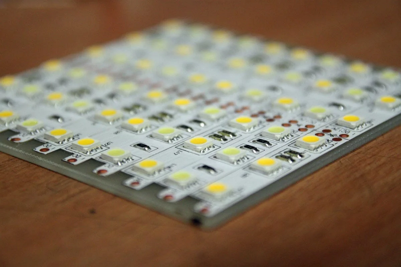
| Typical Applications | Consumer electronics, low-power circuits, and cost-sensitive designs where moderate current suffices | High-power systems (e.g., power supplies, industrial equipment), high-frequency applications to reduce skin effect losses, and scenarios needing enhanced durability |
| Thermal Performance | Less effective for heat dissipation, potentially leading to higher local heating in high-current paths | Superior heat dissipation, minimizing hot spots and improving stability in thermally demanding environments |
| Signal Integrity | Adequate for general-frequency signals but may incur losses in high-frequency designs | Improved performance in high-frequency circuits due to reduced impedance and skin effect |
| Manufacturing Complexity | Simpler and lower-cost etching and processing due to thinner copper layers | More challenging; requires advanced techniques for drilling, plating, and etching, increasing production time and cost |
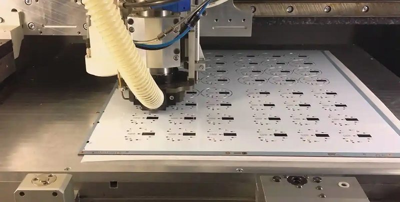
What Is Manufacturing Process of 1 ounce Copper PCB?
Manufacturing Process of 1 ounce Copper PCB:
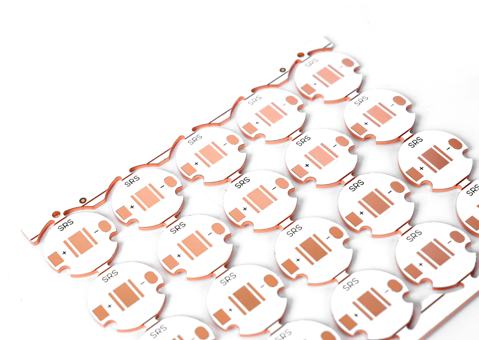
1. Substrate Preparation: Select copper clad laminate (CCL) with substrate material (e.g., FR4, CEM-1) and copper foil thickness of 1oz (35μm). Inspect surface quality (no oxidation, scratches).
2. Inner Layer Circuit Fabrication (Multilayer PCBs):
Clean copper foil → apply photosensitive dry film → expose to transfer circuit pattern → develop to remove unexposed dry film → etch to expose copper → strip dry film, obtaining inner layer circuits.
3. Lamination (Multilayer PCBs): Stack inner layer boards, prepreg (resin sheets), and outer layer copper foils. Press at high temperature and pressure to form a multilayer board.
4. Drilling: Use CNC drill to create through-holes (VIAs, component holes). Clean hole wall debris.
5. Hole Metallization: Chemical copper deposition (thin copper layer on hole walls) → electroplating to thicken copper (ensure hole wall conductivity).
6. Outer Layer Circuit Fabrication:
Clean outer copper foil → apply dry film → expose/develop to form circuit pattern → electroplating to thicken (optional) → etch to remove excess copper → strip dry film, obtaining outer layer circuits.
7. Solder Mask & Silkscreen: Apply solder mask (green oil) → expose/develop to expose pads → print component identifiers (silkscreen).
8. Surface Finish: Apply surface treatment to pads (e.g., HASL for tin spraying, OSP for organic coating, ENIG for nickel-gold plating) to prevent oxidation and improve solderability.
9. Profiling & Testing: Cut to specified size → electrical test (flying probe/ICT) to check circuit connectivity.
10. Packaging & Delivery: Clean PCB surface → vacuum pack → label specifications → ship.

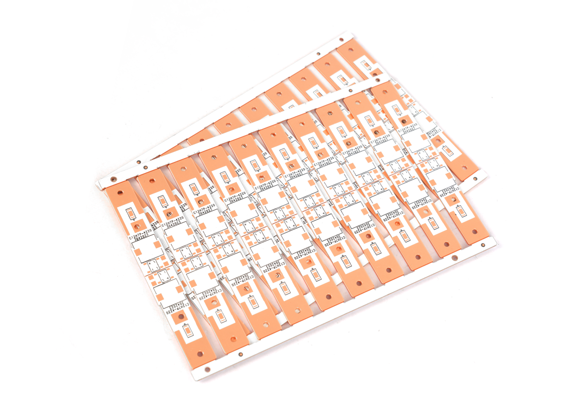
Why Choose EBest Circuit (Best Technology) as Copper PCB Manufacturer?
Reasons why choose us your copper PCB manufacturer:
- Turnkey Solutions – Full-service PCB manufacturing from design to delivery, accelerating your product’s time-to-market.
- Stable Electronics Supply Chain – Guaranteed material availability with minimal risk of delays.
- Superior Quality – 100% inspection on bulk orders, ensuring reliability and consistency.
- Fast Turnaround – 24-hour rapid prototyping and industry-leading production lead times.
- Responsive Support – Dedicated customer service with a 2-hour response guarantee for urgent requests.
- Competitive & Transparent Pricing – No hidden costs, offering the best value without compromising quality.
- Certified Compliance – Fully certified (ISO, RoHS, UL) for global market acceptance.
- 24/7 Engineering Support – Expert thermal management and DFM guidance available anytime.
- Advanced Manufacturing – High-precision etching for optimal 1 oz copper performance.
- Scalable Production – Flexible capacity from prototypes to high-volume orders.
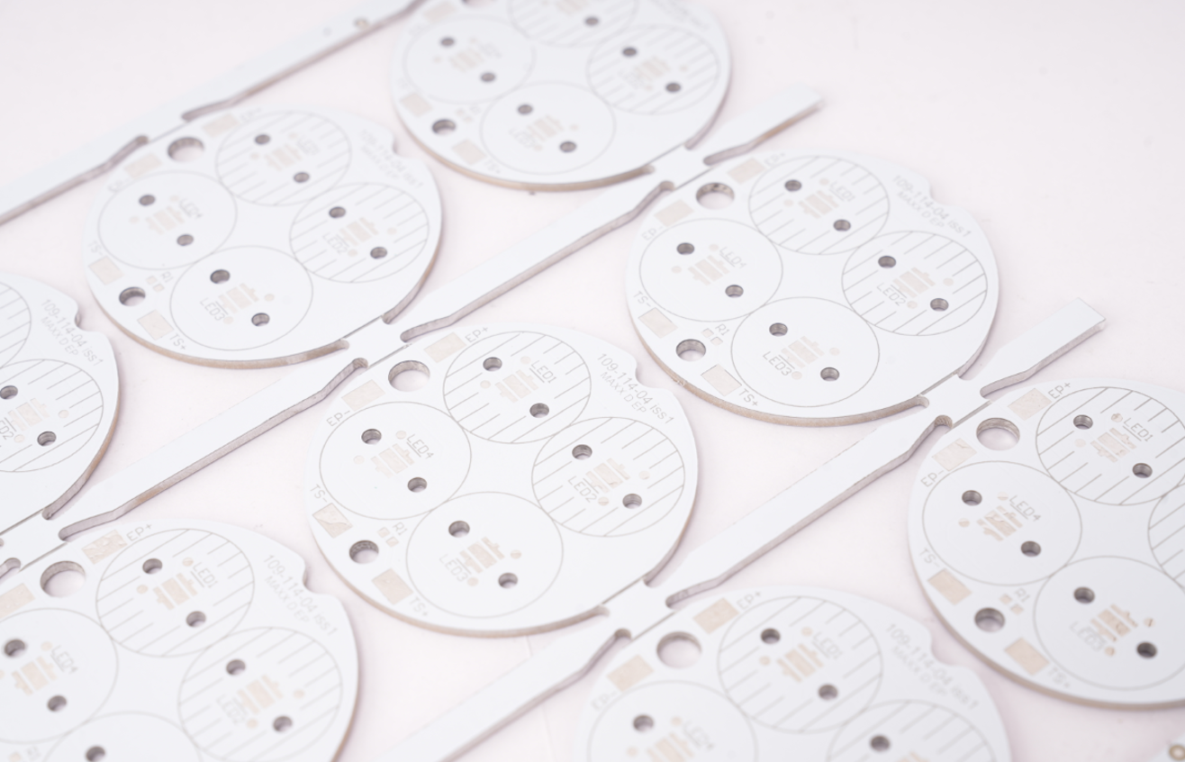
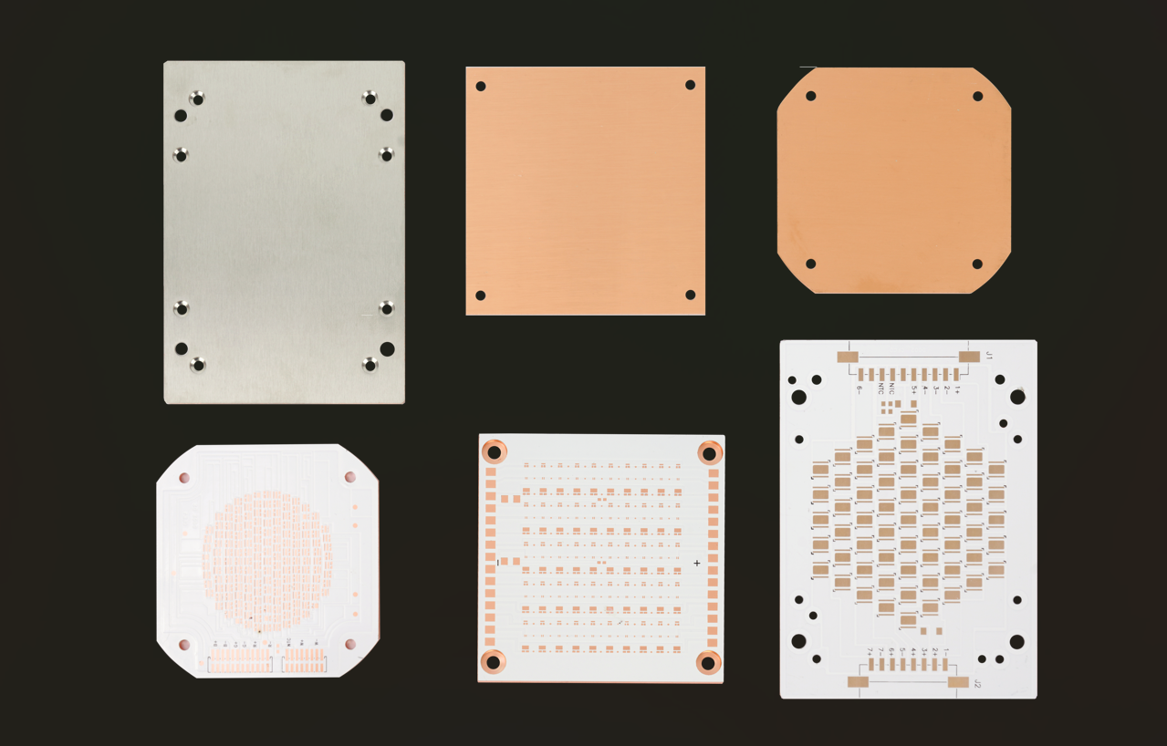
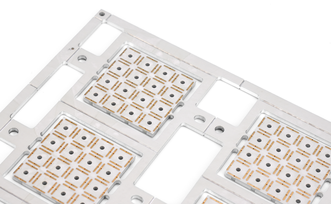
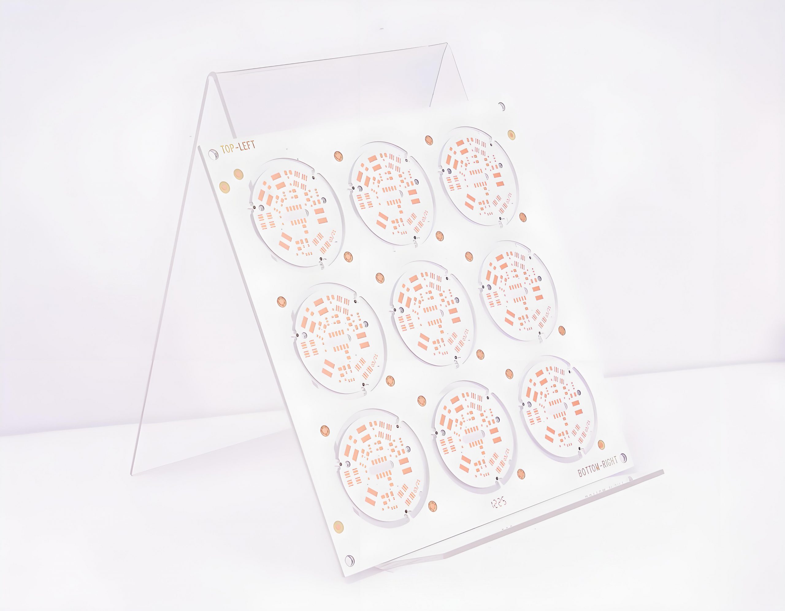
Our Copper PCB Board Capabilities
| Base material | Copper |
| Thermal Conductivity | 0.8, 1.0, 1.5, 2.0, 3.0 W/m.K |
| Board Thickness | 0.5mm~3.0mm(0.02″~0.12″) |
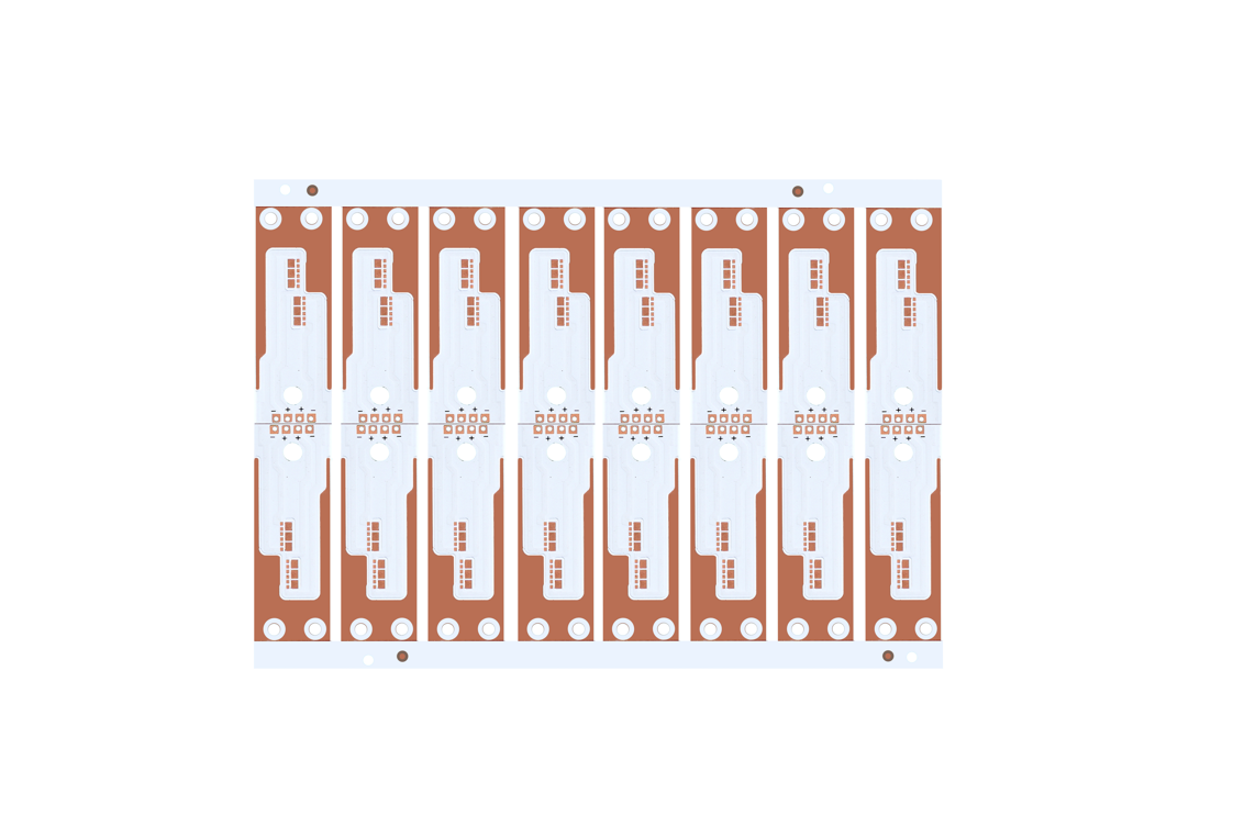
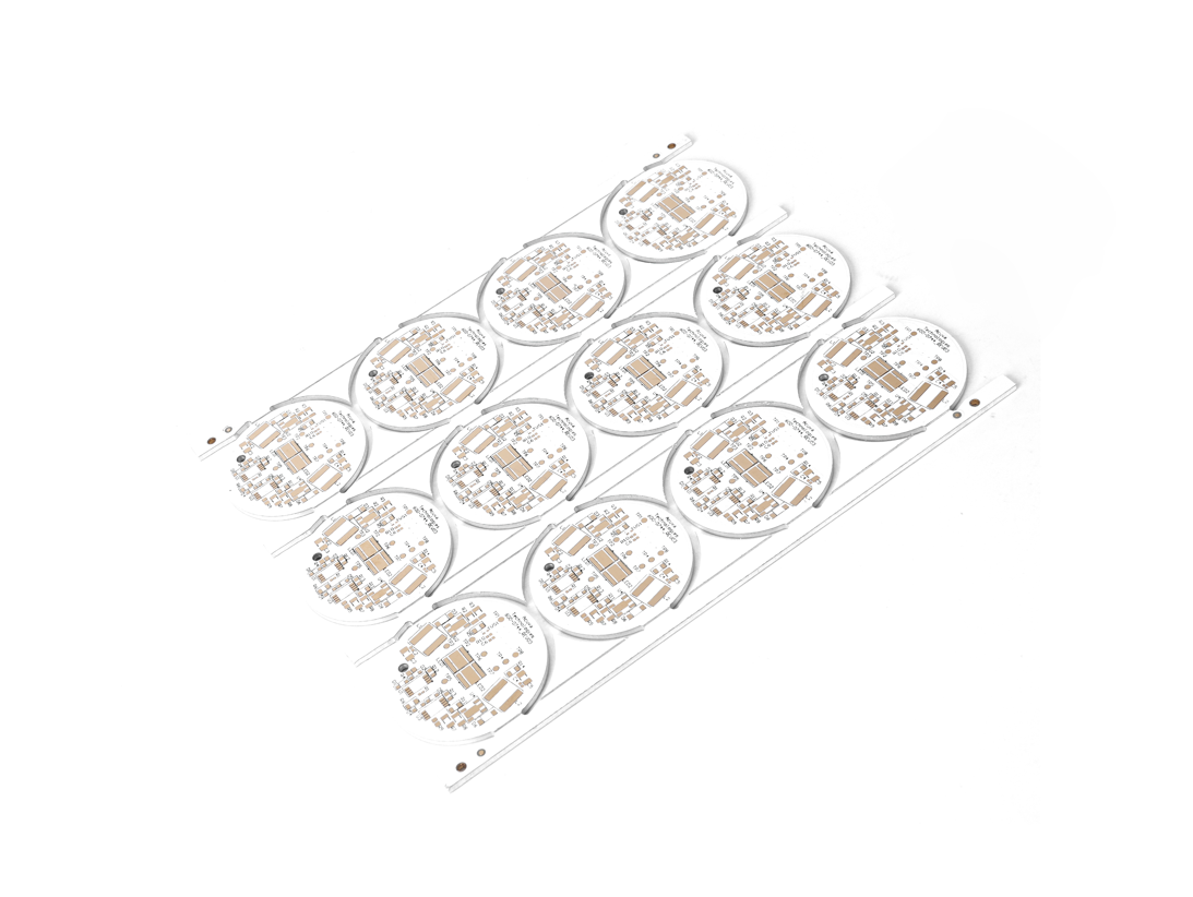
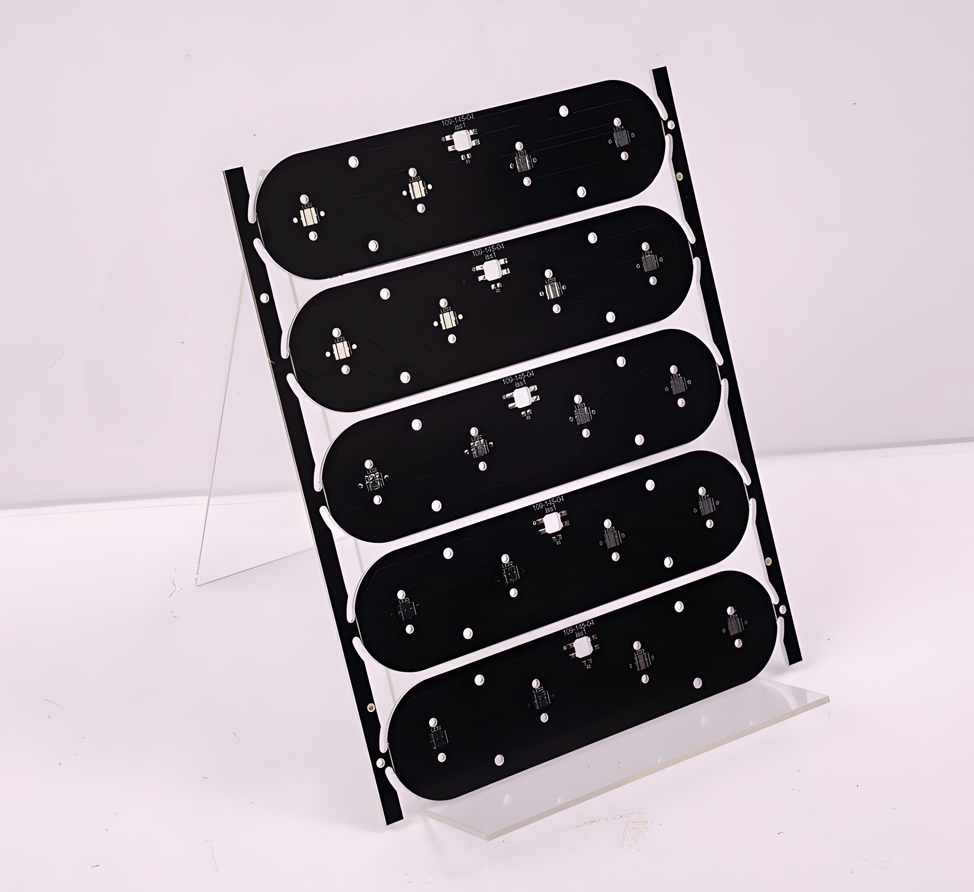
| Copper thickness | 0.5 OZ, 1.0 OZ, 2.0 OZ, 3.0 OZ, up to 10 OZ |
| Outline | Routing, punching, V-Cut |
| Soldermask | White/Black/Blue/Green/Red Oil |
| Legend/Silkscreen Color: | Black/White |
| Surface finishing | Immersion Gold, HASL, OSP |
| Max Panel size | 600*500mm(23.62″*19.68″) |
| Packing | Vacuum/Plastic bag |
| Samples L/T | 4~6 Days |
| MP L/T: | 5~7 Days |
Our Quality Inspection & Certification
- Certified & Compliant Standards: ISO 9001, ISO 13485, IATF 16949, AS9100D Certified, and UL, REACH, RoHS Compliant
- Aging Test (Environmental Stress Screening): Includes thermal cycling (-40℃~85℃) and humidity exposure to validate long-term reliability.
- Dimensional Verification (CMM/Profilometer): Measures thickness (±0.1mm), flatness, and hole alignment accuracy.
- Peel Strength Test (Adhesion Assessment): Quantifies copper-clad laminate bonding force (ASTM D903).
- X-Ray Inspection (Internal Defect Screening): Checks solder joint voids, cracks, and BGA/QFN hidden defects.
- AOI (Automated Optical Inspection): Detects surface defects like open/short circuits, missing components, and soldering issues.
Instant Quote
In summary, 1 oz copper PCBs (35μm thickness) deliver optimal balance between cost and performance for standard applications, with proven current capacity and manufacturing reliability. EBest Circuit (Best Technology) stands out as your ideal partner by offering certified turnkey solutions (ISO/RoHS/UL), 24-hour rapid prototyping, 100% bulk inspection, and engineer-backed thermal management support. Our stable supply chain ensures 2-hour response time and on-time delivery, while transparent pricing eliminates hidden costs. For high-quality 1 oz copper PCBs that accelerate your product development cycle, contact EBest Circuit (Best Technology) today for a competitive quote: sales@bestpcbs.com.