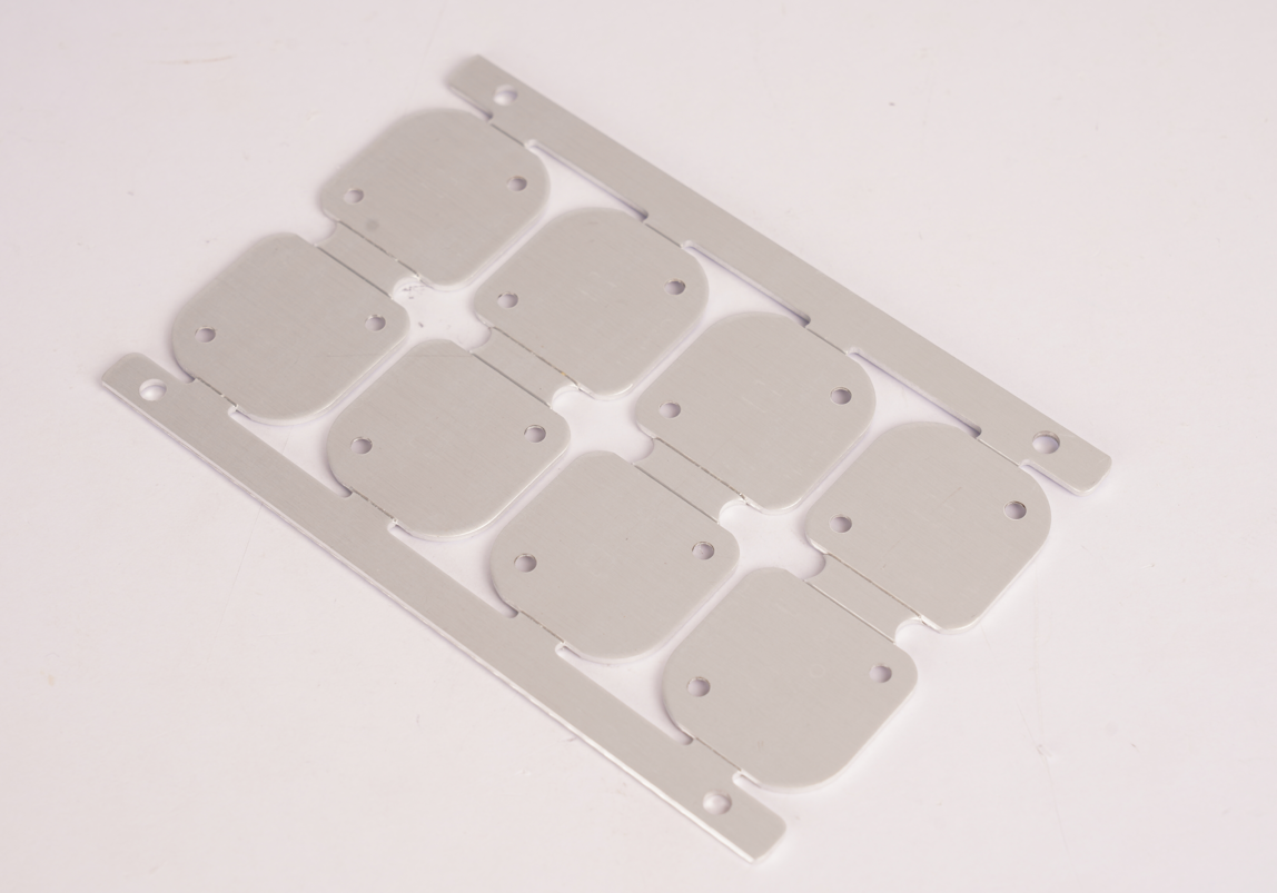
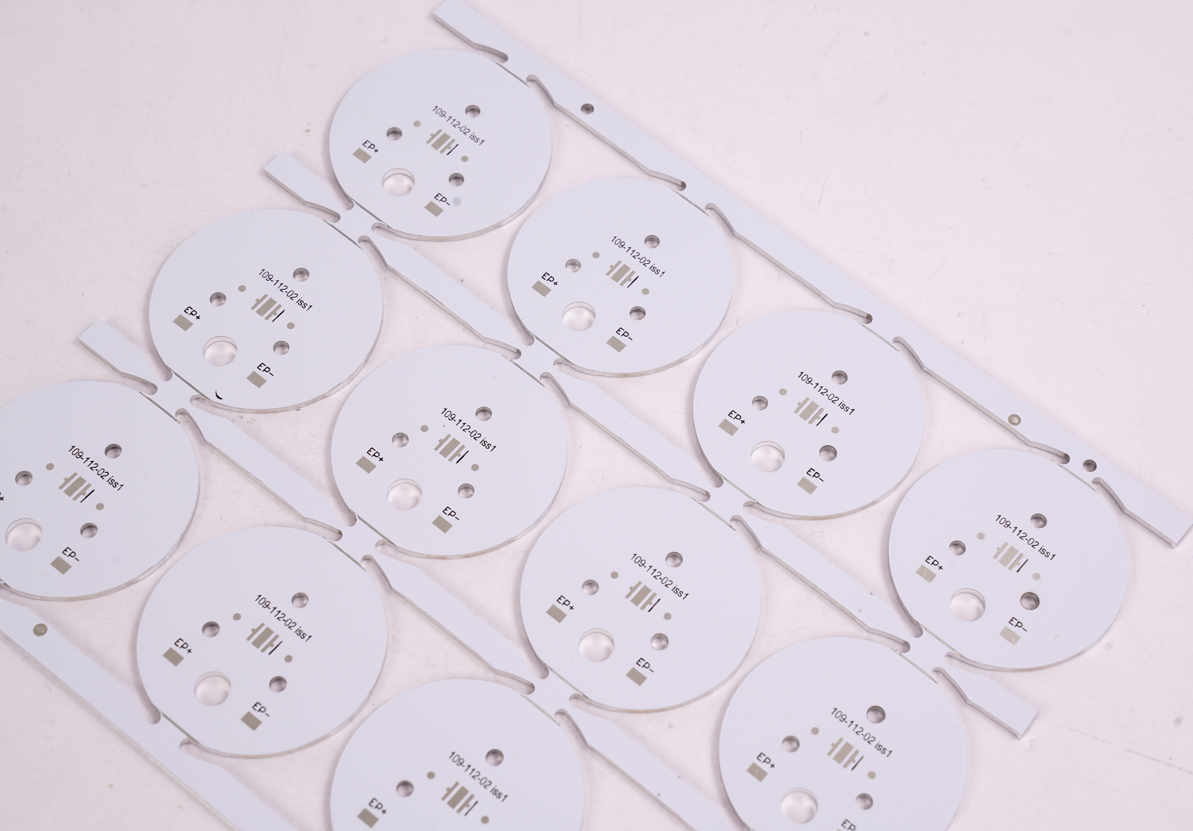
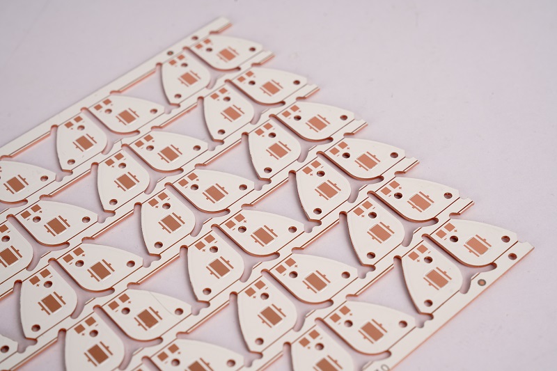
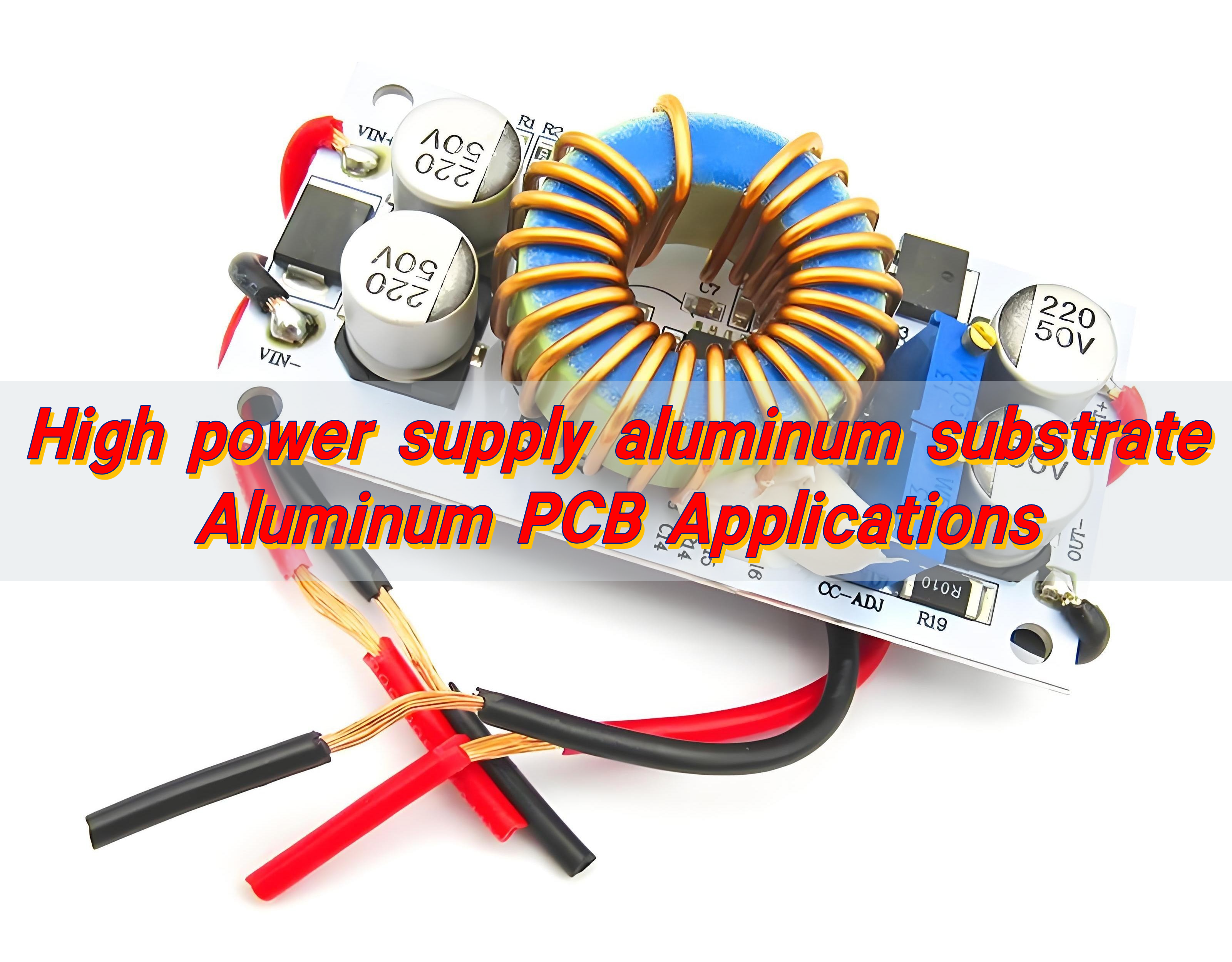
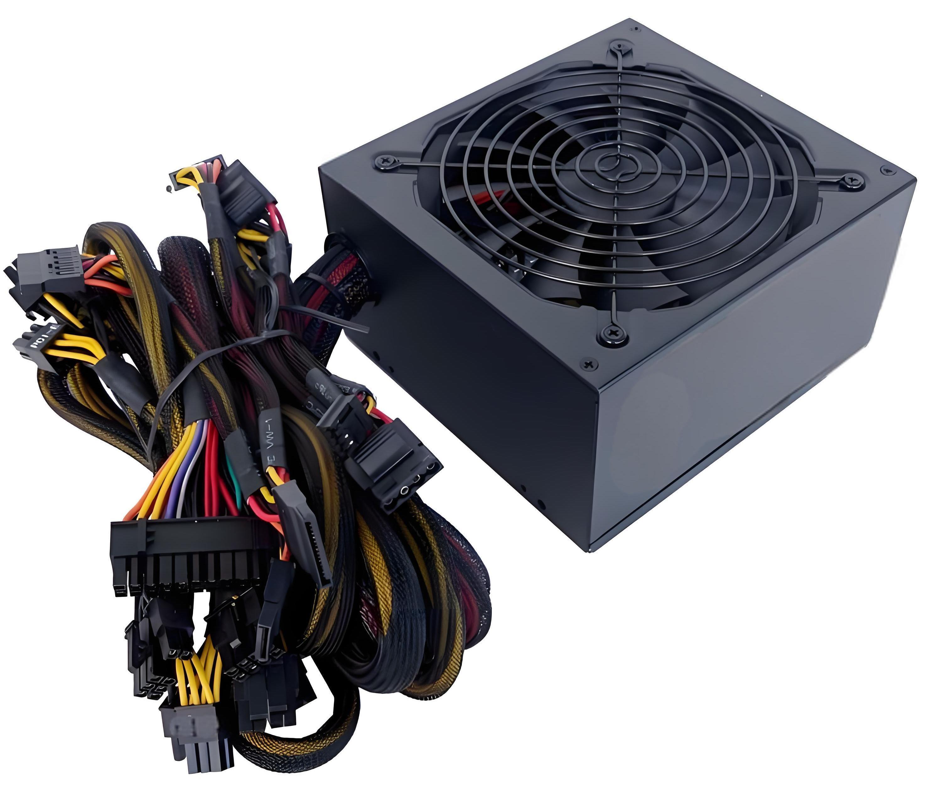
High power supply aluminum substrate offer excellent thermal conductivity, making them ideal for 600W high power supplies, AC power supplies, and other high-energy applications. Using aluminum substrates can improve power supply performance, more effectively manage heat, and extend product life.
Why choose aluminum substrates for high power supply?
Aluminum substrates handle heat like a pro. High power power supplies, especially those above 600W, generate a significant amount of thermal energy. Traditional materials, like FR4, struggle to keep up.
Aluminum substrate PCBs dissipate heat faster and more evenly. This gives you a more stable device. More stability means fewer failures, less stress on components, and longer product life. It’s also why they’ve become the go-to solution for manufacturers looking to build high-performance power supplies for industrial, automotive, LED lighting, and renewable energy systems.
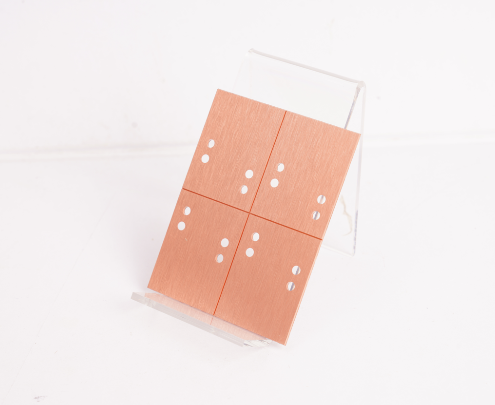
Beyond that, aluminum substrates also provide high mechanical strength. They’re durable. They’re lightweight. They resist moisture and dust. And these are critical factors, especially in environments where power supplies need to run around the clock.
Is a high power AC power supply better with aluminum PCB?
Yes, especially if we’re talking about AC power supplies that operate under heavy loads. High power AC power supplies convert alternating current into usable voltage for machines, lighting systems, or backup power units. The higher the power, the more stress on components. The more heat.
When aluminum PCBs are used in the design, they help control this heat naturally. That reduces the reliance on bulky heatsinks or complex cooling systems. In turn, this minimizes the overall size of the power supply. Product aesthetics improve. And you save space without sacrificing performance.
For example, in data centers or factory automation systems, compact high power AC supplies are in demand. These systems need stability over long periods. With aluminum substrates, the circuit stays cooler. That means the overall supply remains more efficient, even during peak usage.
How do aluminum substrates help heat control in power supply?
Here’s how it works: aluminum substrates have a thermally conductive dielectric layer. This layer sits between the copper circuitry and the aluminum base. As the circuit operates, the heat generated moves through this layer into the aluminum. The metal then acts like a sink, quickly pulling the heat away.
Unlike fiberglass or epoxy boards, aluminum keeps performance stable even as the current surges. Components stay cooler. Solder joints stay intact. And there’s less risk of thermal runaway or damage.
Heat management is one of the most common causes of failure in power electronics. Poor thermal flow can kill a component fast. Aluminum substrate solves this by being a built-in thermal solution.
How does aluminum PCB improve power supply performance?
Better thermal handling doesn’t just keep things cool—it directly boosts power supply performance.
- Fewer Component Failures: By managing it properly, aluminum PCBs reduce component stress. Capacitors, resistors, and semiconductors operate within their safe ranges.
- Greater Power Density: Aluminum substrates can integrate more functions on smaller circuit boards. Its thermal advantages allow for tighter layouts without overheating.
- Higher Efficiency: Less heat means less energy is wasted. Make power more efficient. It consumes less, delivers more, and does so reliably.
- Improved Signal Stability: Heat impacts signal paths, causing drift or noise. With aluminum substrate controlling the temperature, your signals stay sharp and clean.
Do aluminum substrates increase power supply lifespan?
Yes. When temperatures remain in a safe range, the wear and tear on electronic parts is dramatically reduced.
A high power supply running on an aluminum substrate board has a longer operational life. You’ll notice:
- Fewer breakdowns over time
- Longer warranty periods
- Lower maintenance costs
This reliability makes them perfect for mission-critical applications. Think telecom systems, medical devices, or aerospace power controls.
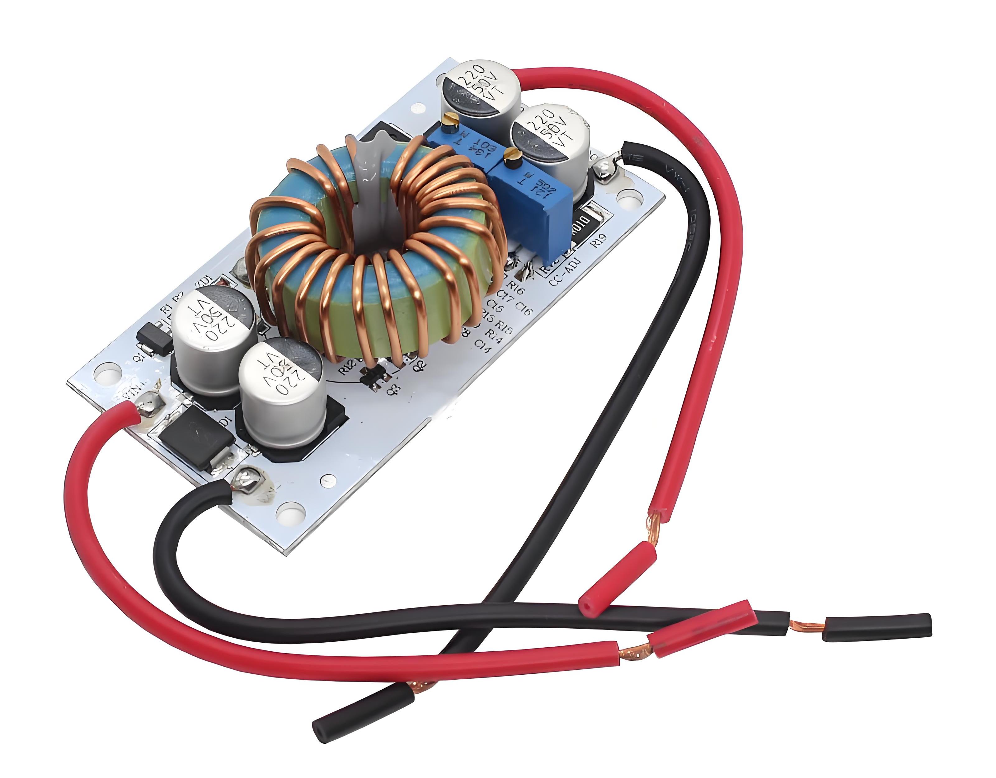
What is a high power power supply 600W used for?
A 600W high power power supply sits at the heart of many mid-to-heavy duty electronic systems. It’s not just about lighting up a circuit—it powers complex machinery. Some typical applications include:
- Industrial automation
- LED lighting arrays
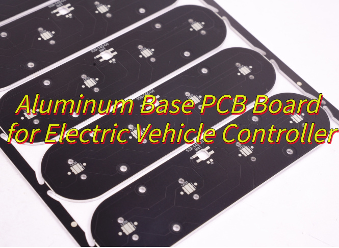
- Electric vehicle systems
- Communication base stations
- Gaming or graphic-intensive computers
- Security surveillance networks
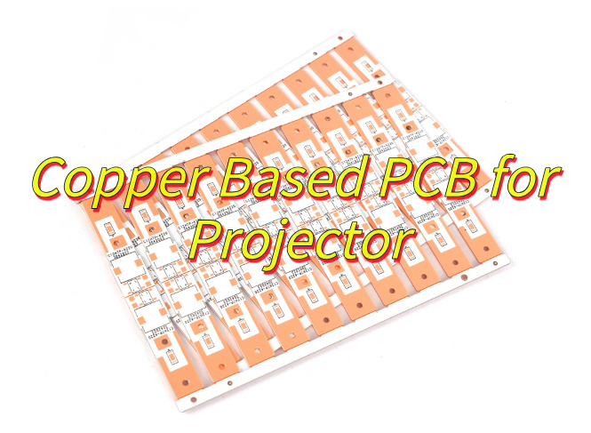
What other applications are there for aluminum substrate PCB?
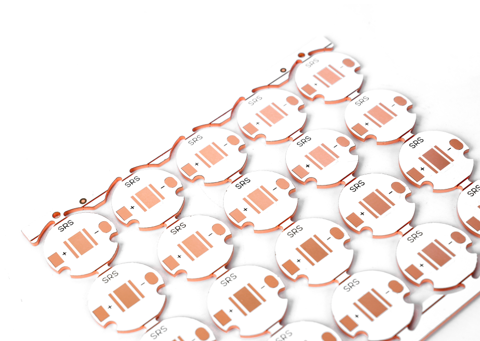
The applications don’t end with power supplies. Aluminum substrate PCBs are widely used across industries.
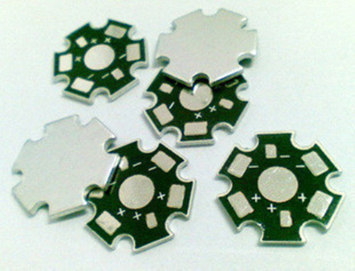
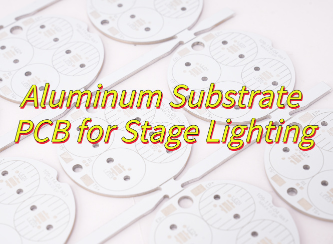
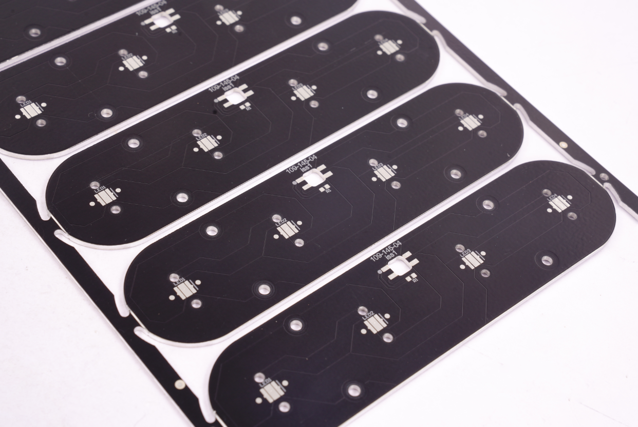
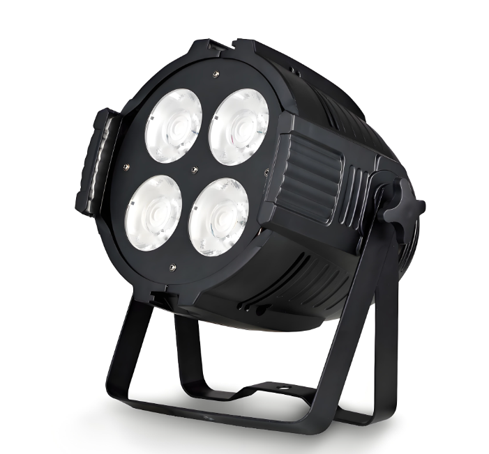
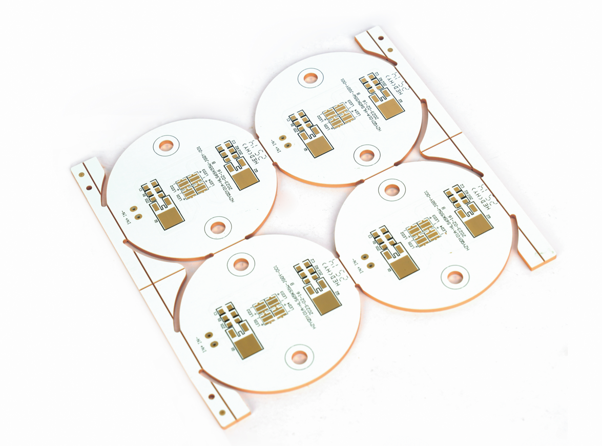
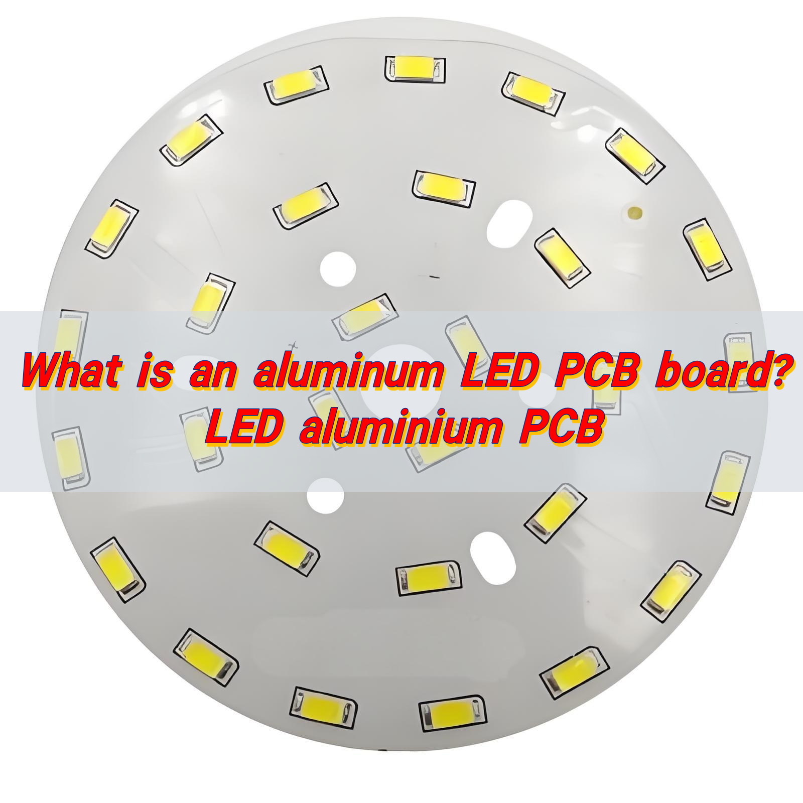
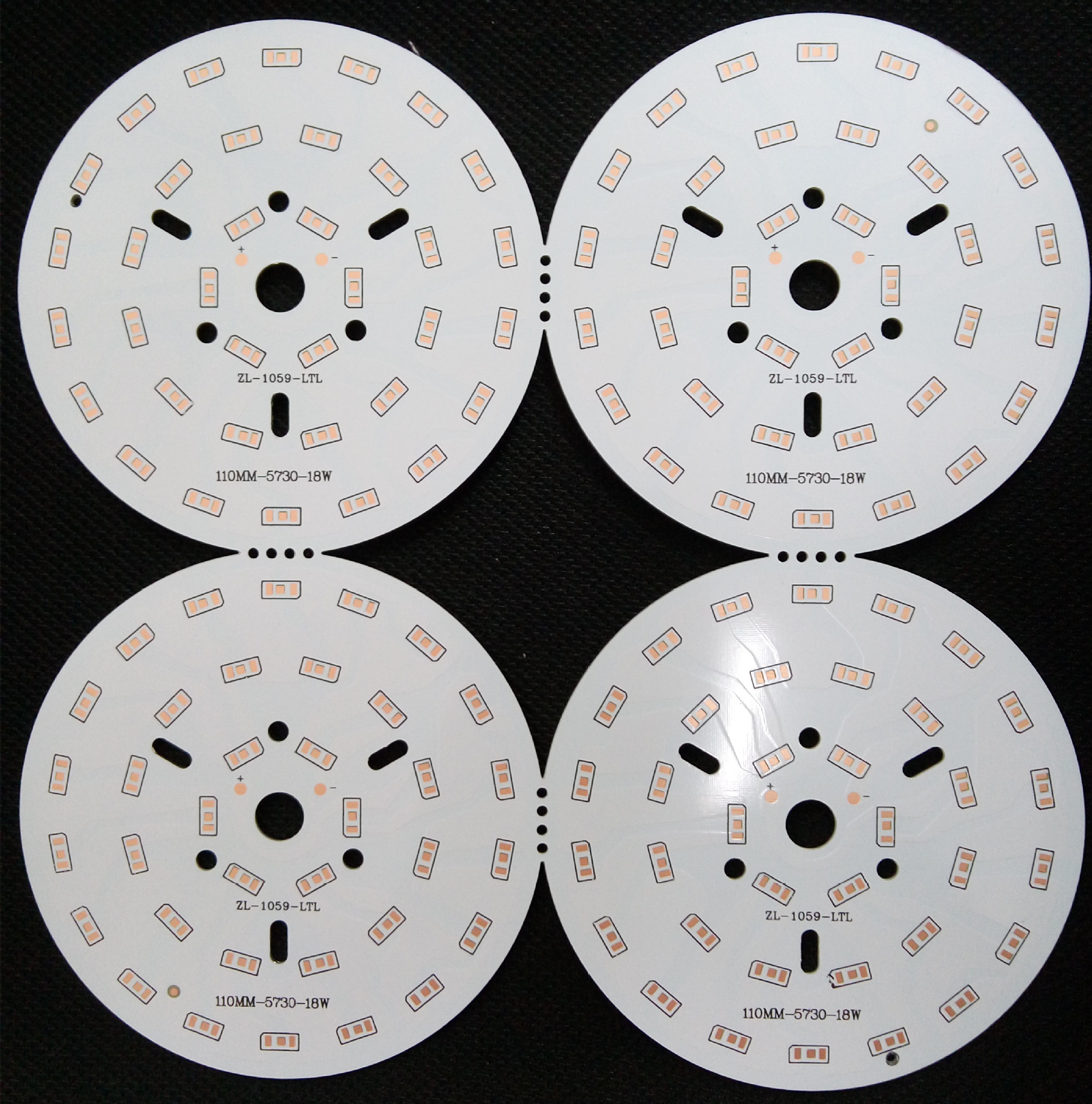
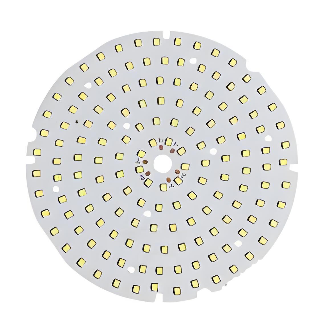
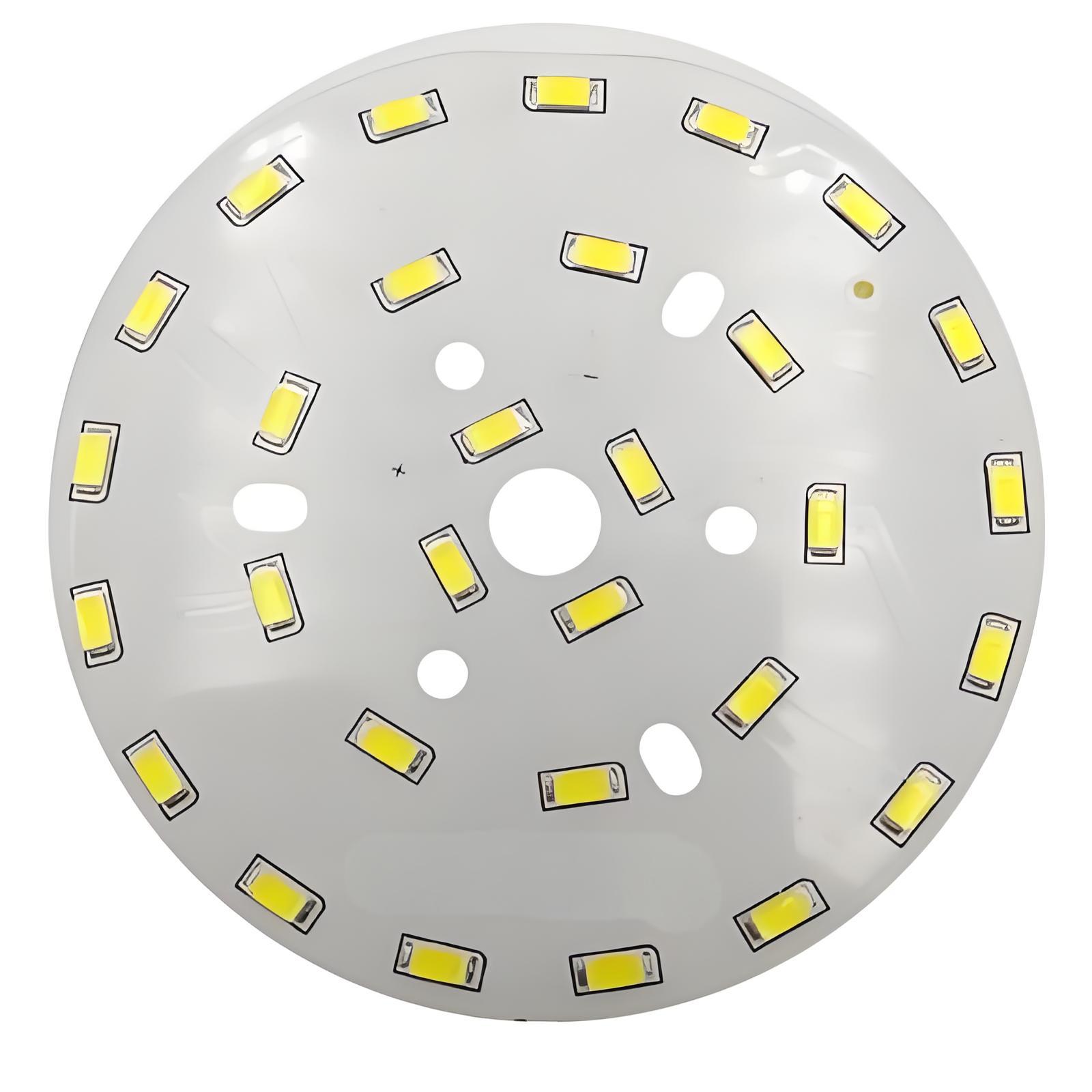
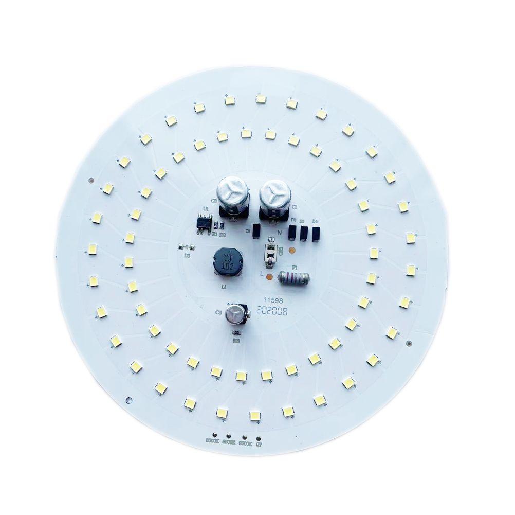
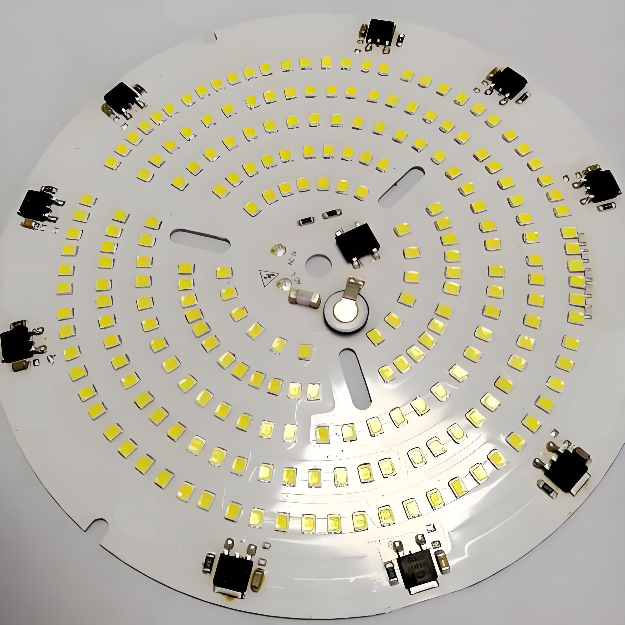
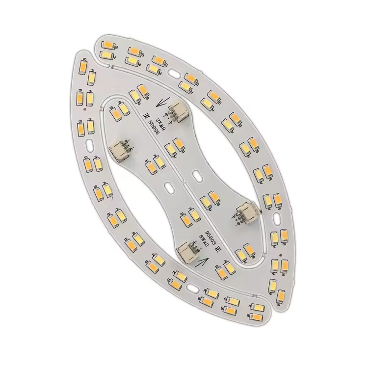
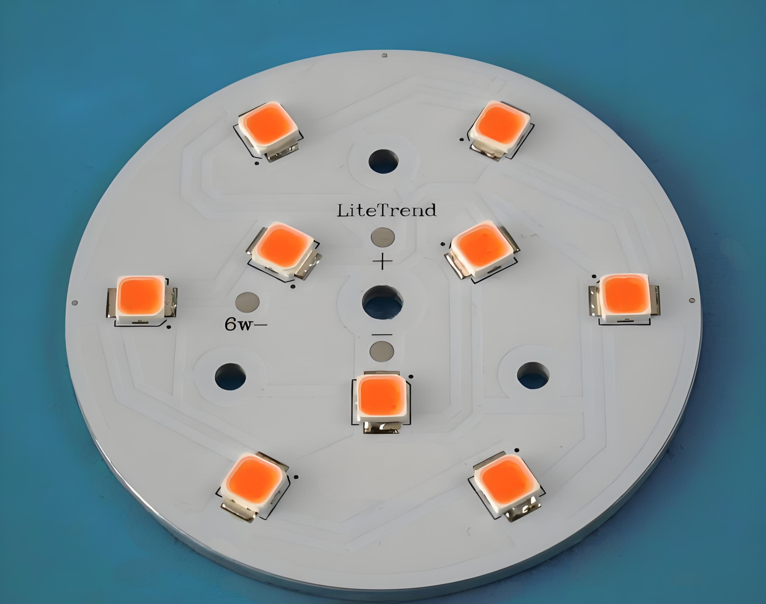
- LED Lighting Modules: Aluminum PCB is the backbone of modern LED lighting. It boosts brightness and improves lifespan.
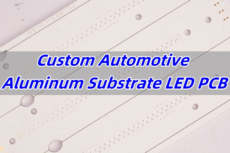
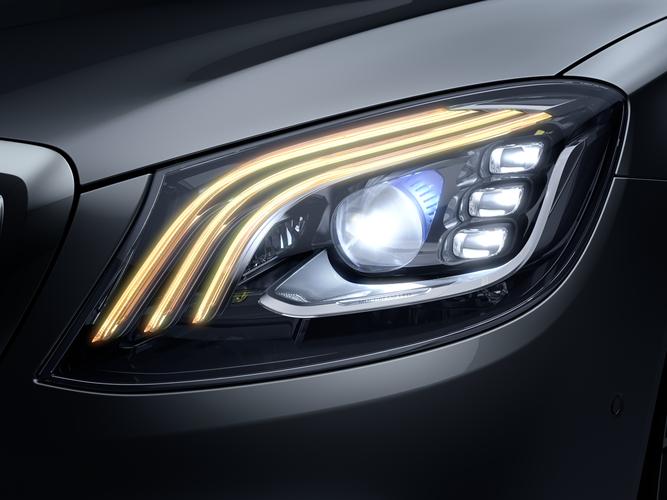
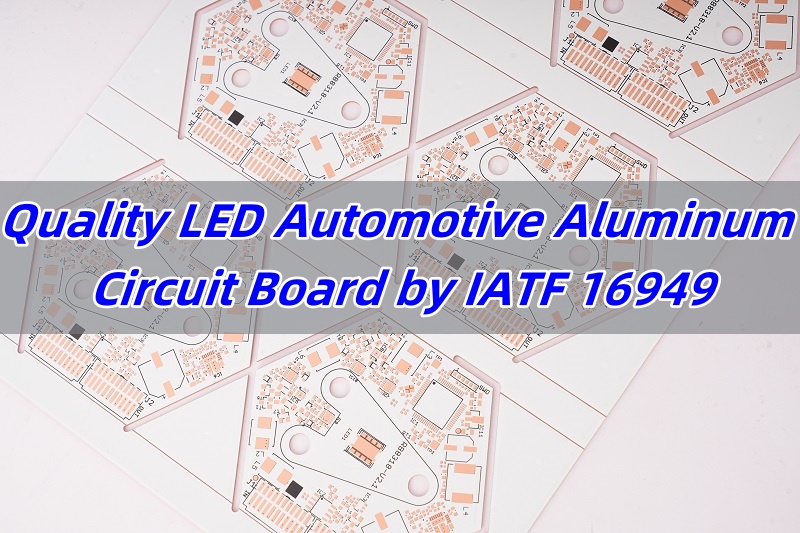
- Automotive Electronics: From headlights to power control units, aluminum PCBs handle the intense thermal conditions in vehicles.
- Solar Power Systems: Inverters and battery controllers often use aluminum substrates for maximum efficiency.
- Medical Equipment: Aluminum substrates help maintain consistent performance in imaging devices and diagnostic tools.
- Military and Aerospace: Aluminum substrates stand up to shock, vibration, and extreme temperatures.
Why choose BEST Technology aluminum PCB supplier?
When you’re working on a high power power supply or any other thermal-sensitive application, BEST Technology is your best choice.
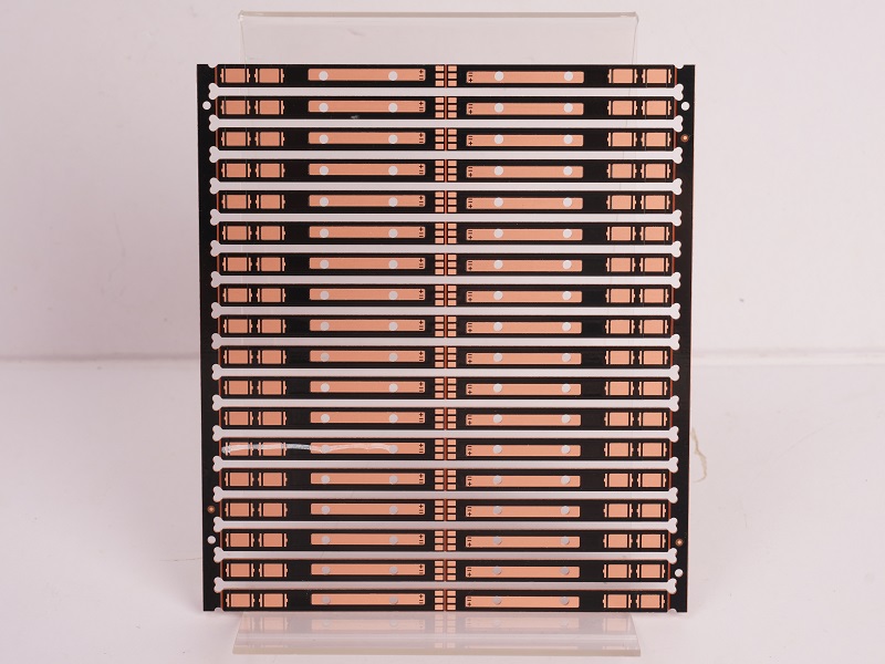
With nearly two decades of experience in aluminum PCB manufacturing, BEST Technology has positioned itself as one of the most trusted suppliers in China. We specialize in high-quality, performance-driven solutions for power electronics.
Why choose us?
- Advanced Production Capabilities: From single-layer aluminum PCBs to complex multi-layer structures, we manufacture with precision.
- Custom Engineering Support: Need a custom stack-up or layout? Our expert engineers work closely with you to meet exact specs.
- Consistent Quality Assurance: We follow ISO9001:2015 standards, and all aluminum PCBs undergo strict electrical and thermal testing before shipment.
- Fast Turnaround Times: We deliver prototypes in days—not weeks—so you can move your project forward without delays.
- Competitive Pricing: Top quality doesn’t have to mean top dollar. Our pricing is optimized for value, especially on volume orders.
- Global Delivery: Whether you’re in Asia, North America, or Europe, we ship globally and ensure safe, on-time delivery.
At BEST Technology, we don’t just provide PCBs—we help power your innovation. Whether you’re developing a 600W supply or a full-scale industrial controller, Our aluminum substrate designs can meet your needs
Conclusion:
High power supply aluminum substrates offer excellent heat control, improve power supply performance, and extend lifespan. With reliable thermal management and mechanical strength, aluminum substrate PCB is widely used in LED lighting, automotive, and industrial equipment.
BEST Technology is a leading aluminum PCB manufacturer in China, trusted for reliable quality, fast delivery, and expert support. We help you create high-performance power supply solutions that last.
Contact us today at sales@bestpcbs.com to discuss your aluminum PCB needs.