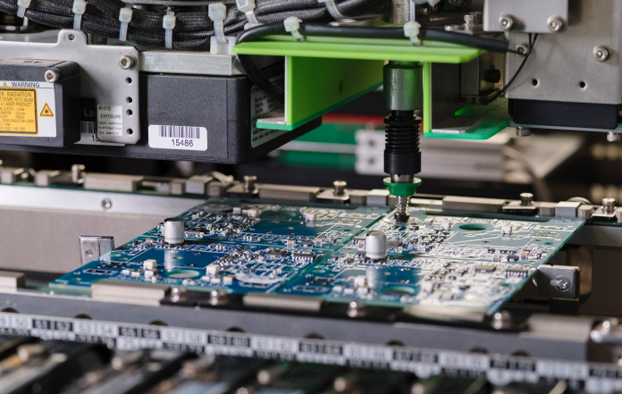
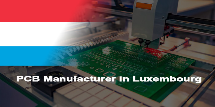
Hungary has emerged as a key hub for electronics manufacturing in Eastern Europe, attracting numerous PCB Hungary manufacturer and global firms setting up local production bases. As a professional PCB Hungary manufacturer, EBest Circuit Co., Limited (Best Technology Circuit Co., Limited) leverages local industrial advantages and global supply chain resources to deliver high-quality PCB Hungary solutions. The region’s PCB manufacturing sector benefits from labor cost advantages and proximity to European markets, while facing challenges like process consistency and supply chain stability that demand reliable Hungary PCB manufacturer partners.

Are You Facing These Challenges?
- Are your PCB designs frequently rejected due to manufacturability issues, leading to repeated revisions and project delays?
- Are you unable to find a Hungarian PCB factory that can provide 24-hour expedited prototyping services for small-batch, time-sensitive orders?
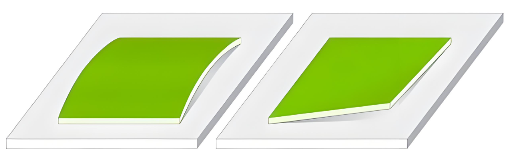
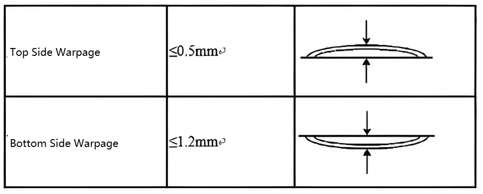
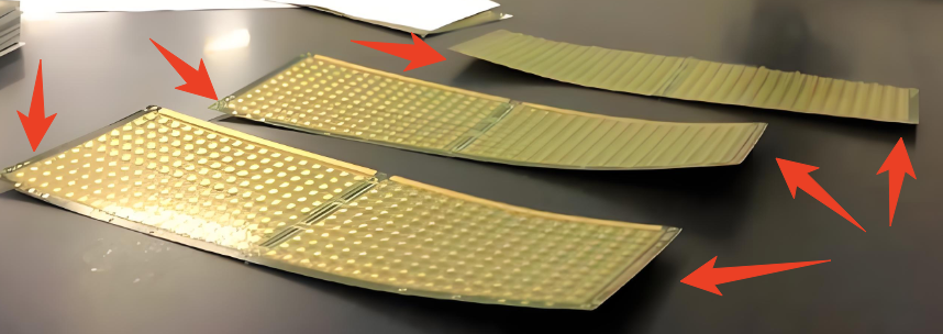
- Do you encounter board warping and deformation issues after lamination or reflow soldering, affecting assembly yield?
- Do you frequently experience communication difficulties with local Hungarian PCB companies, resulting in mismatched production requirements?
- Are high raw material costs and exchange rate fluctuations making it difficult to control your Hungarian PCB manufacturing costs?
- Is the quality inspection of your mass-produced PCBs insufficient, leading to a risk of defects after delivery?
- Are you unable to obtain timely technical support in Hungary for specialized processes such as HDI or thick copper PCB manufacturing?
End-to-End Guarantee from Requirement to Delivery
- Pre-Production Consultation: Provide free DFM analysis to identify design flaws in advance, avoiding revision delays and reducing Hungary PCB manufacturing costs. Our professional team delivers analysis reports with clear optimization suggestions for seamless cooperation.
- Urgent Prototyping Support: 24-hour rapid prototyping service for time-sensitive orders, ensuring your project progresses as scheduled without waiting for standard lead times. We leverage global production resources to fulfill urgent demands for PCB Hungary projects.
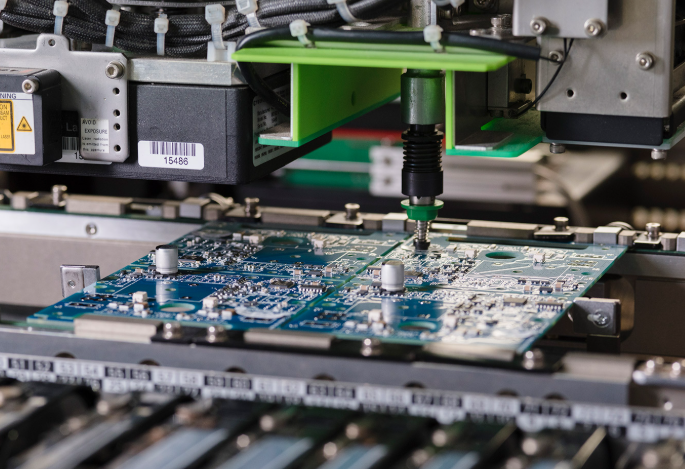
- Process Optimization: Adopt symmetric lamination and precise temperature control to eliminate board warpage, improving assembly yield for PCB Hungary products. Strict process parameters are standardized to ensure consistent quality across batches.
- Dedicated Account Management: Assign exclusive account managers to handle your orders, providing scheduled progress updates and prompt responses to inquiries via email and phone. We ensure production requirements are accurately implemented through our global production network for Hungary-bound orders.
- Cost Control: Offer cost-sensitive solutions based on 19 years of experience, optimizing material selection and process flow to offset raw material and exchange rate impacts. Customized plans help reduce overall Hungary PCB manufacturing costs effectively.
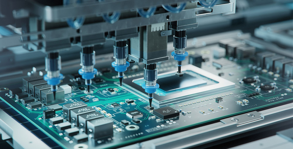
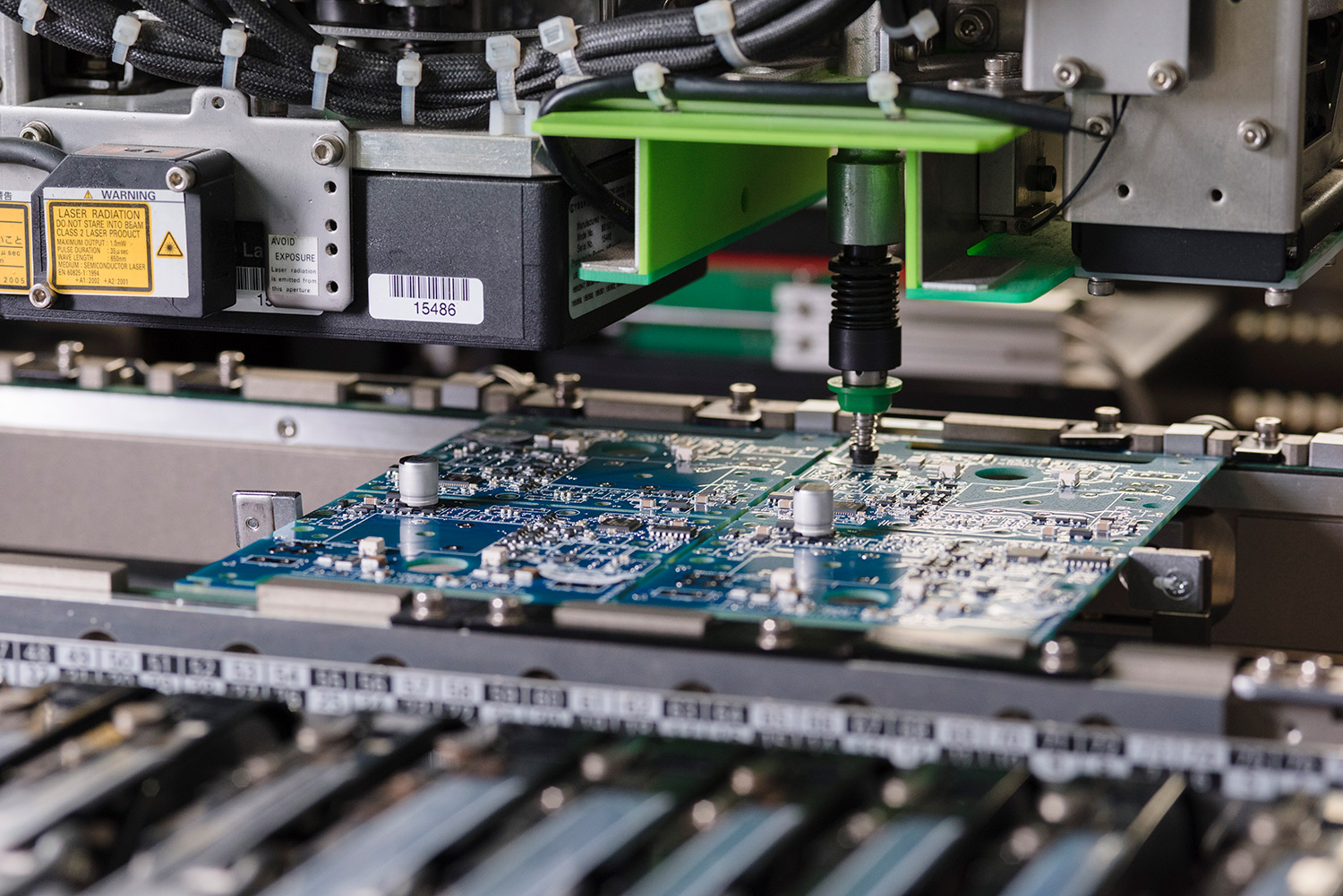
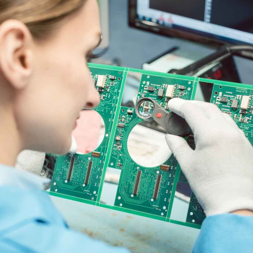
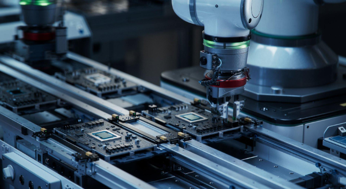
- Full Inspection for Mass Production: Implement 100% AOI and X-Ray inspection in our PCB manufacturing process for Hungary orders, eliminating defective products before delivery. Inspection reports are provided to confirm quality compliance.
- Special Process Capability: Master HDI, thick copper, and rigid-flex PCB technologies, with a professional technical team to solve bottlenecks. We support complex process requirements for Hungary PCB manufacturing projects.
- On-Time Delivery Commitment: Rely on mature global supply chain management and automated production lines to achieve a 99.2% on-time delivery rate. Cross-border logistics optimization ensures timely arrival of PCB Hungary orders.
Why Hungarian Clients Choose EBest (Best Technology) for PCB Manufacturer?
- 19 Years of Industry Experience: Rich expertise in solving complex manufacturing challenges, helping customers reduce trial-and-error costs and shorten time-to-market.
- Free DFM Analysis: Professional design review before production, identifying potential issues to avoid rework and improve Hungary PCB manufacturing efficiency.
- 24-Hour Urgent Prototyping: Dedicated production lines for emergency orders, completing PCB Hungary prototyping within 24 hours to meet tight project schedules.
- Authoritative Certifications: Hold ISO9001:2015, ISO13485:2016, IATF16949, REACH, and RoHS certifications, meeting requirements for medical, automotive, and industrial electronics.
- Competitive Pricing & Cost-Saving Solutions: Customized cost-sensitive plans based on project requirements, reducing overall Hungary PCB manufacturing costs by 15%-20% through process optimization.
- High On-Time Delivery Rate: 99.2% order punctuality supported by MES production management system, ensuring stable supply for your production line.
- Strict Quality Control: 100% full inspection for mass production, adhering to strict quality control processes that exceed industry standards for PCB Hungary products.
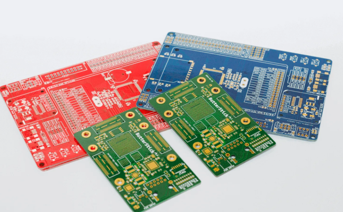
Top 10 PCB Manufacturers in Hungary
| Company Name | Main Business | Core Advantages | Process Capability | Lead Time |
| EBest Circuit Co., Limited (Best Technology Circuit Co., Limited) | PCB prototyping, mass production, assembly, and custom solutions for Hungary market | 24-hour urgent service, 99.2% on-time rate, multiple EU certifications, cross-border logistics optimization | HDI, thick copper, rigid-flex, 1-20 layers PCB, 100% AOI/X-Ray inspection | Prototyping: 24hrs; Mass production: 3-7 days (Hungary-bound delivery) |
| Electrohungária Kft. | Industrial PCB manufacturing, assembly and testing for automotive electronics | IATF16949 certification, local supply chain, EU RoHS compliance | 1-12 layers, thick copper (up to 4oz), SMT assembly, functional testing | Prototyping: 4-6 days; Mass production: 7-10 days |
| PCB Tech Hungary Zrt. | High-precision PCB prototyping and medium-volume production for industrial control | ISO9001:2015 certified, fast technical response, local after-sales support | 1-16 layers, HDI, buried/blind vias, impedance control (±5%) | Prototyping: 3-5 days; Mass production: 6-9 days |
| Hungarocircuits Kft. | Custom PCB manufacturing and turnkey solutions for medical devices | ISO13485:2016 certification, sterile production environment, REACH compliant | 1-10 layers, rigid PCB, metal core PCB, biocompatible surface finishes | Prototyping: 5-7 days; Mass production: 8-12 days |
| Euroelektro Kft. | Small-batch PCB manufacturing and assembly for consumer electronics | Competitive pricing, online order tracking, local logistics partnership | 1-8 layers, standard surface finishes (HASL, ENIG), SMT/DIP assembly | Prototyping: 2-4 days; Mass production: 5-8 days |
| TechPrint Magyarország Kft. | High-frequency PCB manufacturing for telecom and aerospace industries | Specialized in high-frequency materials (PTFE, Rogers), strict tolerance control | 1-14 layers, high-frequency PCB, microwave PCB, minimum line width 0.1mm | Prototyping: 6-8 days; Mass production: 10-14 days |
| Magyar PCB Zrt. | Large-volume PCB production for automotive and industrial automation | Automated production lines, 98.5% on-time rate, bulk material cost advantages | 1-12 layers, rigid PCB, high-temperature resistant materials, wave soldering | Prototyping: 4-6 days; Mass production: 7-11 days |
| ProCircuit Hungary Kft. | Custom rigid-flex PCB manufacturing and complex assembly solutions | Rigid-flex technical expertise, ISO9001/ISO13485 dual certification | 1-16 layers, rigid-flex PCB, flexible circuits, mixed-technology assembly | Prototyping: 7-9 days; Mass production: 12-15 days |
| NeoCircuits Magyarország Kft. | PCB prototyping and low-volume production for startups and R&D projects | Flexible order terms, technical consulting, fast prototype iterations | 1-10 layers, standard PCB, quick-turn prototyping, basic functional testing | Prototyping: 2-3 days; Small-batch: 4-6 days |
| Metalkirály Kft. | Metal core PCB manufacturing for LED and power electronics applications | Excellent thermal conductivity, RoHS/REACH compliant, local material sourcing | 1-8 layers, metal core PCB (aluminum, copper core), thermal simulation support | Prototyping: 5-7 days; Mass production: 8-10 days |
How to Choose a Reliable PCB Hungary Manufacturer?
Below is A Selection Guide to PCB Hungary Manufacturer:
- Verify Certification Compliance: Confirm IATF16949 (automotive) and ISO13485 (medical) certifications. Ensure EU RoHS (lead ≤0.1%) and REACH compliance, aligning with your product category to avoid penalties from misaligned credentials (impacting 12% of local orders yearly).
- Test Urgent Prototyping Capability: Validate 24-hour quick-turn services via small trials. Confirm dedicated lines, ≥99.2% urgent prototyping yield, and transparent costs with urgent fees at 15%-30% of standard pricing. Avoid hidden fees with detailed quotes covering all process costs.
- Review Quality Control Details: Request AOI (≥99.8% surface defect coverage) and X-Ray (≥99.5% BGA joints accuracy) data. Target batch defect rate ≤0.05% (half the 0.1% industry average), and clarify 48-hour quality response and replacement for batches over 0.03% defects.
- Confirm Process Suitability: Ask for verifiable Hungary project cases for HDI, thick copper or high-frequency PCBs. Ensure impedance tolerance ±5%, micro-drill tolerance ±0.01mm, layer alignment error ≤5μm, and dielectric constant 3.5-4.5 for high-frequency PCBs.
- Assess Delivery Stability: Check 12-month on-time rate ≥98% (exceeding the 95% local average). Inquire about supply chain contingencies, including local core material stock (minimum 2 weeks) and logistics partners with ≥99% on-time rates, plus ≤2% annual disruption rate.
- Prioritize Value-Added Services: Optimize for free 1-hour DFM analysis, which cuts rework rates from 8%-12% to ≤3%. Ensure ≥95% 24-hour resolution for complex processes; DFM analysis also shortens lead time by 3-5 days on average.
- Analyze Total Cycle Costs: Beyond unit prices, account for rework (7% of order value), late fees (1%-2% daily), packaging (2%-5%), and EU customs duties (0%-6%). Prefer 3-6 month price locks to mitigate volatility, as copper prices fluctuate ±18% yearly.
- Clarify Communication Norms: Set 24-hour email response timelines and 99.9% accurate notifications for key order nodes. Define 8-hour confirmation for order adjustments, reducing delays from miscommunication (affecting 6% of orders).
How to Evaluate Production Capacity of PCB Hungary Manufacturer?
Evaluation Guide to Production Capacity of Hungary PCB Manufacturer:
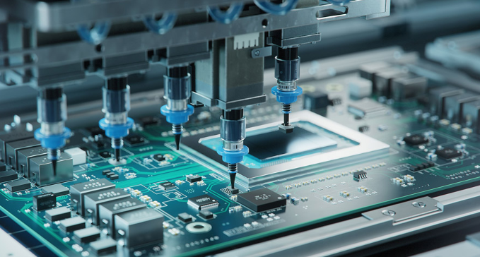
- Inspect Equipment Precision & Efficiency: Verify automated SMT lines with ≥60,000 components/hour placement speed and ±0.03mm precision, AOI machines with ≥99.8% surface defect coverage, and micro-drilling equipment supporting minimum 0.1mm diameter with ±0.01mm tolerance.
- Review Process Parameter Limits: Confirm maximum production layers (1-20 layers for high-capacity Hungary PCB factory), minimum line width 0.075mm, and minimum hole diameter 0.1mm, with impedance tolerance controlled within ±5% for high-frequency products.
- Evaluate Daily Capacity & Batch Adaptability: Assess daily output (5,000-50,000 pieces for mass production, 100-500 pieces for small-batch) and order handling capability, ensuring ≤24-hour response for batches ≤500 pieces and stable yield ≥99.2% across batch sizes.
- Check Supply Chain Stability: Confirm cooperation with top-tier material suppliers (e.g., Isola, Rogers for substrates; JX Nippon for copper foil), core material inventory ≥14 days, and supplier on-time delivery rate ≥99% to avoid production interruptions.
- Assess Process Optimization Efficiency: Evaluate multi-variety order changeover time (≤2 hours for different PCB types) and process optimization effects, such as yield improvement ≥3% and production cycle reduction ≥15% via smart process adjustment.
- Verify Quality Management Effectiveness: Check batch defective rate ≤0.05% (industry average 0.1%), customer complaint rate ≤0.3%, and ISO9001:2015-certified QMS with monthly quality review mechanisms.
- Quantify Technical Problem-Solving Capacity: Confirm technical team size (≥15 professionals for mid-sized Hungary PCB manufacturer), complex process problem-solving rate ≥95%, and resolution time ≤24 hours for HDI/thick copper PCB issues.
- Evaluate Scheduling & Urgent Order Flexibility: Ensure MES-based production scheduling system with real-time tracking, ≤2-hour response to urgent orders, and ability to handle ≤30% urgent orders without affecting standard order on-time rate (≥98%).
How to Evaluate Delivery Time of Hungary PCB Manufacturer?
Evaluation Guide to Delivery Time of Hungary PCB Manufacturer:
- Confirm standard delivery times: Clearly define delivery times for different order types and layer counts – prototyping (1-8 layers: 2-5 days; 10+ layers: 7-10 days) and mass production (1-8 layers: 3-8 days; 10+ layers: 10-15 days), consistent with the average standards of the Hungarian PCB manufacturing industry.
- Assess urgent order handling capabilities: Verify 24/48-hour delivery capabilities, with urgent order fees at 15%-30% of the standard price. Ensure on-time delivery rate for urgent orders is ≥99%, and that a dedicated production line is available to support up to 30% of daily capacity.
- Check on-time delivery rate: Require an on-time delivery rate of ≥98% over 12 months, higher than the local industry average of 95%. Require detailed data, with delays due to logistics reasons accounting for ≤60% and delays due to production reasons accounting for ≤40%.
- Assess supply chain resilience: Confirm safety stock of core materials (copper foil, substrates) is ≥14 days. Ensure annual logistics disruption rate is ≤2%, and that an emergency plan for raw material shortages is in place with a 48-hour recovery capability.
- Review scheduling transparency: Ensure real-time tracking based on the MES system, with order status updated every 4 hours. Require order visualization coverage of ≥99%, and respond to scheduling adjustment requests within 8 hours.
- Inquire about delay contingency plans: Inquire about the capacity of backup production lines (which can be activated within 2 hours), representing 20% of total capacity. Clearly define delay compensation terms, typically 1%-2% of the order value per day.
- Evaluate logistics partners: Verify that logistics partners have an on-time delivery rate of ≥99%. Confirm domestic delivery time in Hungary is within 24 hours, and cross-border delivery time in Europe is within 48-72 hours, with logistics costs ≤5% of the order value.
- Check communication efficiency: Ensure delay notifications are sent within 2 hours of discovering a delay. Require delivery milestone reminder coverage of ≥99.5%, and respond to status inquiry emails within 24 hours.
FAQs of Hungary PCB Manufacturing
Q1: How to solve board warpage problems during Hungary PCB manufacturing?
A1: We adopt symmetric lamination design and precise temperature control during reflow soldering (heating rate ≤2℃/sec, cooling rate ≤1℃/sec) to eliminate internal stress. Our pre-production DFM analysis also optimizes copper distribution to prevent warpage. Contact us for customized process solutions for your PCB Hungary project.
Q2: Why do design files often cause production delays, and how to avoid it?
A2: Common issues include unclear layer definitions and insufficient pad spacing. We provide free DFM analysis to check design files within 1 hour, identifying and correcting flaws in advance. Our team will also offer optimization suggestions to ensure smooth Hungary PCB manufacturing. Inquiry now for free file review.
Q3: How to control costs when raw material prices and exchange rates fluctuate?
A3: With 19 years of experience, we offer cost-sensitive solutions by optimizing material selection and process flow. We also lock in material prices for long-term cooperation and share cost-saving tips. Choose our PCB manufacturing service Hungary to stabilize your budget. Contact us for a quotation.
Q4: What to do if urgent prototyping is needed within 24 hours for a small-batch order?
A4: Our Hungary PCB plant has dedicated urgent production lines, completing 24-hour prototyping for 1-20 layers of PCB. We also provide door-to-door delivery in Hungary to save time. Reach out now to start your urgent PCB Hungary order.
Q5: How to ensure quality consistency for mass-produced PCBs?
A5: We implement 100% AOI optical inspection and X-Ray detection for BGA solder joints, with a strict three-stage quality control process. Our batch defective rate is controlled below 0.03%, meeting high industry standards. Trust our PCB Hungary manufacturer for stable quality—send your inquiry today.