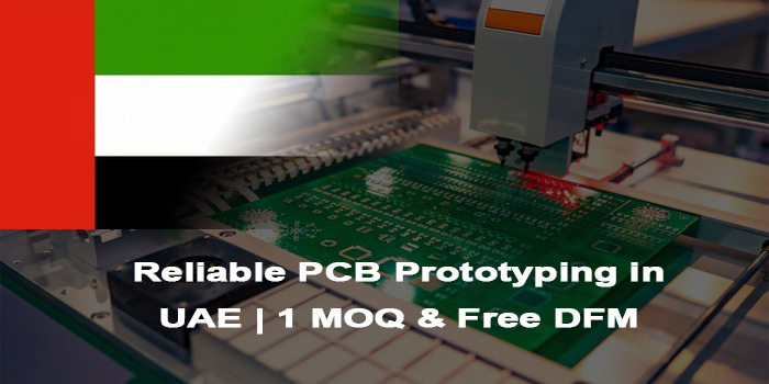
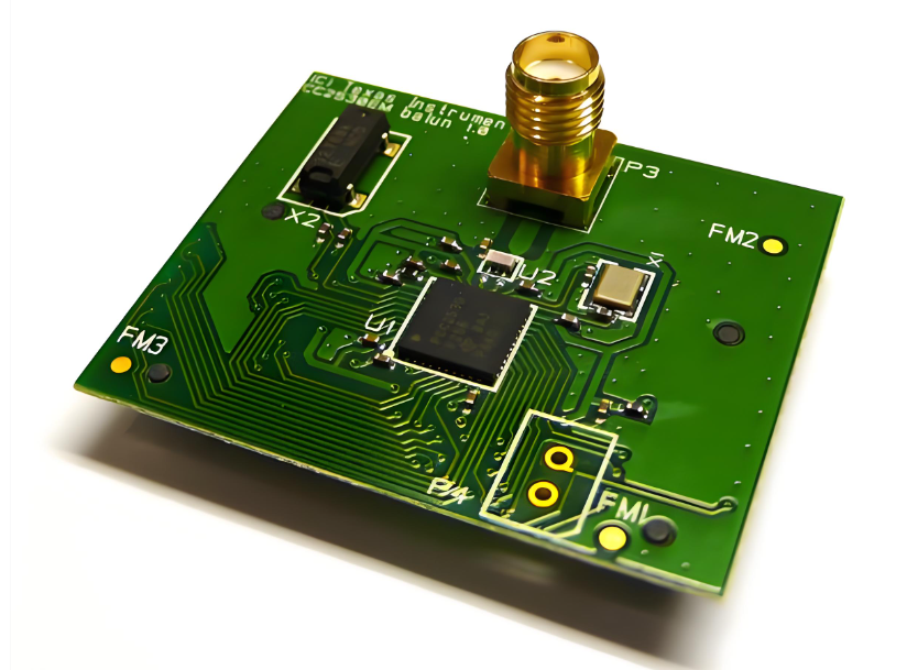
PCB prototyping in Pakistan turns electronic designs into functional products, and EBest delivers tailored, high-precision solutions built for local needs. Our focus on PCB prototyping in Pakistan means every sample adheres to strict quality standards, with fast turnaround and personalized support to navigate the unique challenges of the region’s electronic manufacturing landscape.

Are You Facing These Pain Points of PCB Prototyping in Pakistan?
- Can local PCB prototyping services meet the high precision requirements for medical and aerospace components?
- Is it possible to get urgent PCB prototypes delivered within 24 hours in Pakistan?
- Do local providers offer reliable component sourcing for custom PCB prototyping projects?
- Can PCB prototypes be customized to fit specific industrial equipment or medical device specifications?
- Are there PCB prototyping services in Pakistan that provide free design checks to avoid production errors?
- Do local manufacturers maintain consistent quality for small-batch PCB prototyping orders?
- Can production data for PCB prototypes be tracked to ensure transparency and accountability?
EBest’s Solutions to Pakistan’s PCB Prototyping Pain Points
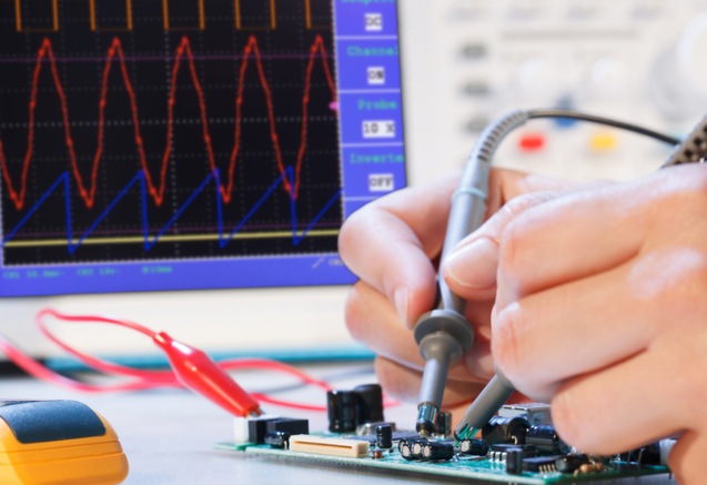
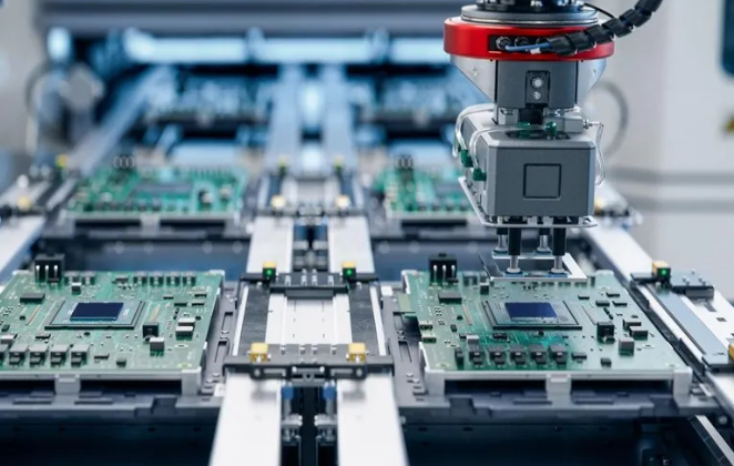
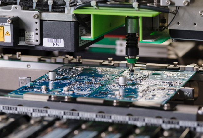
To solve precision challenges in PCB prototyping in Pakistan, we use advanced manufacturing equipment. We include LDI exposure machines, precision laser drilling equipment and automated pressing systems to ensure tight tolerances and consistent quality that meets medical and aerospace industry standards. Our 24-hour expedite service is supported by dedicated production lines. This enables us to deliver urgent PCB prototypes in Pakistan within the required timeframe and keep your projects on track without unnecessary delays.
We offer end-to-end component sourcing through our rigorously managed global supplier network. All vendors undergo strict qualification audits, sample testing and ongoing performance evaluations to ensure high-quality components for custom PCB prototyping projects. This removes the burden of sourcing from local clients. It saves them time and reduces supply chain risks. Our team also provides fully customized solutions by tailoring PCB prototypes to the unique specifications of industrial equipment, medical devices and other specialized applications.
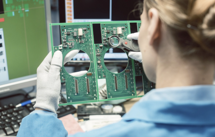
Every PCB prototyping order includes free DFM analysis. Our engineers review designs to identify potential flaws such as component spacing issues, impedance mismatches or manufacturing constraints. They also provide actionable adjustments to reduce errors and rework. We maintain consistent quality across all order sizes from small batches to large runs. We use standardized production processes and certified quality management systems including ISO 9001, ISO 13485 and AS9100D. Our MES system enables full production data tracking to let you monitor every stage of the PCB prototyping process for complete transparency.
Why Choose EBest for PCB Prototyping in Pakistan?
Here are reasons why choose EBest for PCB prototyping in Pakistan:
- Our 19+ years of PCB prototyping experience means you get tried-and-tested expertise for your projects in Pakistan, reducing risks of errors and ensuring your prototypes align with your goals from the start.
- A first article success rate of over 95% saves you time and resources by minimizing rework, avoiding costly delays to your project timeline and ensuring your PCB prototypes work as intended on the first try.
- Our 24-hour fast prototyping service lets you meet tight deadlines for PCB prototyping in Pakistan, keeping your projects on schedule and preventing costly hold-ups in your product development or launch.
- A 99.2% order on-time delivery rate ensures your PCB prototypes arrive exactly when you need them, eliminating production bottlenecks that could slow down your operations or delay your projects.
- With a low MOQ and 1 piece minimum order, you can access high-quality PCB prototyping for small projects, R&D, or trial runs without overspending, perfect for testing designs before scaling up.
- Customized PCB prototyping services adapt to your unique design needs, whether for medical, aerospace, or industrial applications, so your prototypes fit your specific product requirements perfectly.
- Free DFM analysis catches design issues early, helping you avoid expensive mistakes, reduce rework costs, and keep your PCB prototyping process smooth and efficient.
- ISO 9001, ISO 13485, and AS9100D certifications guarantee your PCB prototypes meet global industry standards, ensuring compliance for your products and giving you confidence in their quality.
- MES system integration for full production data tracking keeps you informed at every step, giving you transparency and control over your PCB prototyping order and peace of mind.

What Types of PCB Prototyping Service in Pakistan Can We Provide for You?
Types of PCB prototyping service in Pakistan we can provide for you:
- Flexible PCBs: Ideal for compact, high-flexibility applications in medical devices and portable electronics.
- Rigid PCBs: Durable and stable, suitable for industrial equipment, aerospace components, and standard electronic devices.
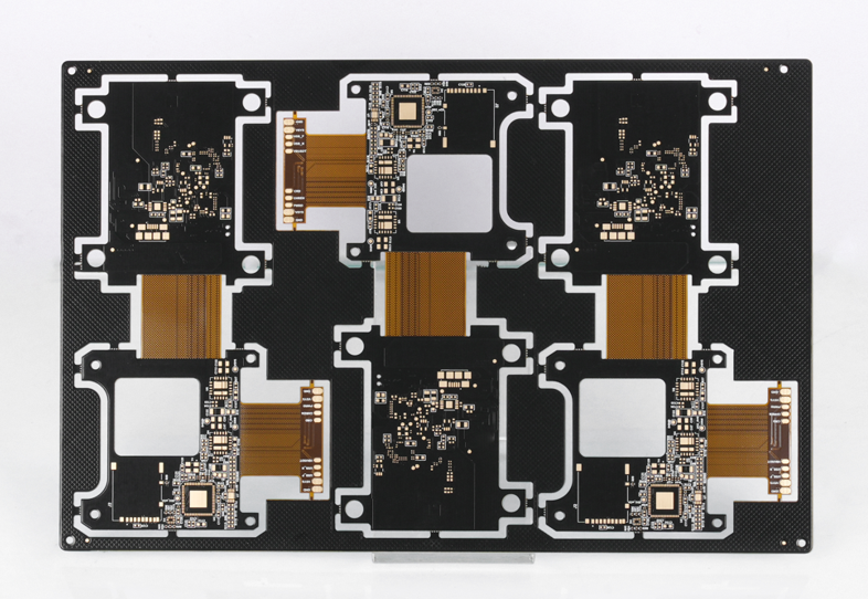
- Rigid-Flex PCBs: Combine the flexibility of flexible PCBs with the stability of rigid PCBs, perfect for complex, space-constrained designs.
- Ceramic PCBs: High-temperature resistance and excellent thermal conductivity, ideal for medical and aerospace applications.
- Metal Core PCBs (MCPCBs): Superior heat dissipation, suitable for high-power electronic components and industrial equipment.
- High-Frequency PCBs: Optimized for signal integrity, used in aerospace, communication, and industrial control systems.
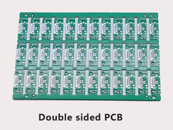
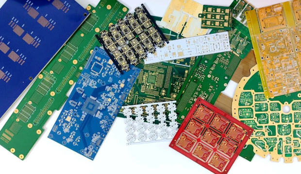
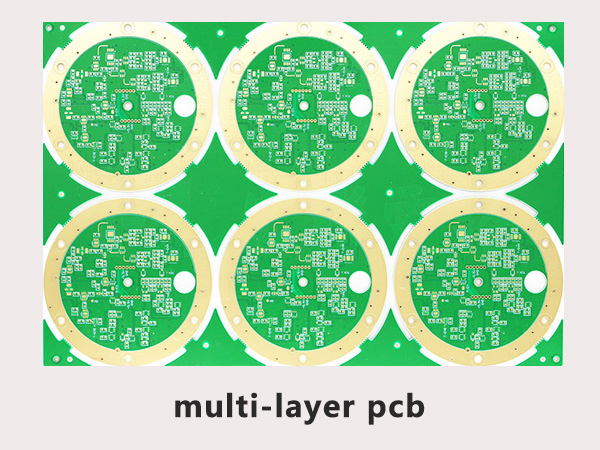
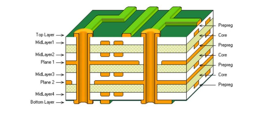
- Additional types: FR4 PCBs, single-sided PCBs, multi-layer PCBs, HDI PCBs, heavy copper PCBs, and impedance control PCBs.
High-Quality PCB Prototyping in Pakistan: EBest’s Quality Control Process
Below are our quality control process for high quality PCB prototyping in Pakistan:
- Pre-production DFM analysis: Free design review by our engineering team to identify potential manufacturability issues. This step ensures PCB prototypes align with design specifications and can be produced efficiently without costly rework.
- Raw material inspection: All materials including substrates and components undergo rigorous testing. We verify quality consistency and compliance with global industry standards to ensure they meet the durability and performance needs of your PCB prototypes.
- In-process quality checks: Regular inspections are conducted during printing drilling and assembly. These checks maintain precision control and consistency across every stage of production to avoid defects.
- SPI (Solder Paste Inspection): 3D optical inspection measures solder paste thickness with a tolerance of less than ±10%. This ensures uniform solder application prevents poor connections and eliminates short circuits or cold solder joints.
- AOI automatic optical inspection: 9-second per-board analysis uses high-resolution imaging to detect soldering defects component misalignment and other visual anomalies. This fast accurate check ensures no flaws are missed before final testing.
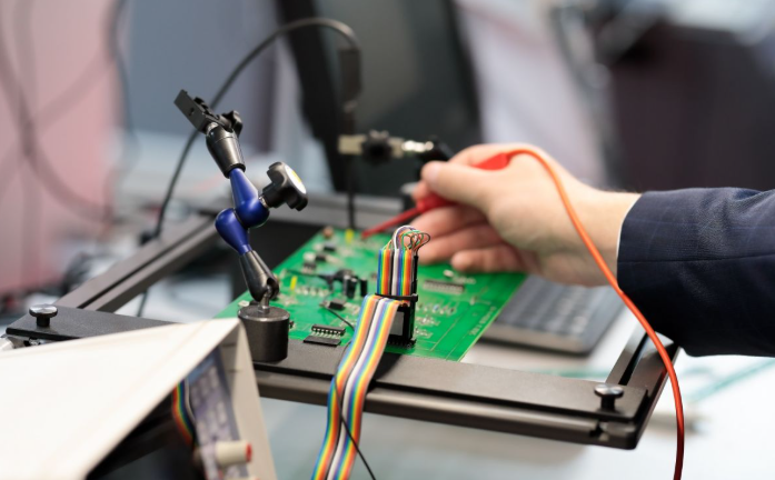
- Electrical testing: Flying probe testing and functional testing are performed to verify PCB prototype performance and connectivity. These tests confirm all electrical pathways work as intended and meet design requirements.
- Final inspection: A comprehensive review of all PCB prototypes is completed before delivery. This ensures each unit meets our strict quality standards and aligns with your specific project requirements.

How EBest Ensures On-Time Delivery for PCB Prototyping Orders in Pakistan?
This is how we ensures on-time delivery for PCB prototyping orders in Pakistan:
- Advanced production scheduling: Our MES system integrates with smart scheduling tools to optimize PCB prototyping workflows, aligning order priorities with equipment capacity and production constraints to minimize bottlenecks and ensure efficient, on-schedule processing of every order.
- Dedicated expedite team: A specialized team focuses solely on urgent orders, prioritizing 24-hour PCB prototyping in Pakistan requests and leveraging streamlined workflows to meet tight deadlines without compromising quality or precision.
- Supplier collaboration: We maintain long-term partnerships with rigorously vetted component suppliers, conducting regular quality audits and performance evaluations to ensure timely availability of high-quality materials for your PCB prototyping projects.
- Real-time order tracking: Our MES system lets you monitor every stage of your PCB prototyping order from design review and production to packaging and shipping, providing real-time updates to keep you informed and in control.
- Contingency planning: We maintain backup production lines and pre-qualified alternative component sources to quickly mitigate delays caused by unexpected equipment issues or supply chain disruptions, keeping your PCB prototyping on track.
- Streamlined logistics: We partner with trusted shipping providers with proven experience delivering to Pakistan, ensuring fast, reliable transit of your PCB prototypes while maintaining product integrity during shipping.

EBest’s Pakistan Medical PCB Prototyping Project Case Study
Project Background
A Pakistan-based medical device manufacturer needed PCB prototypes for a portable patient monitoring device a Class II medical product requiring compliance with ISO 13485 standards. The client struggled with local PCB prototyping services that failed to meet precision requirements and missed delivery deadlines delaying their product launch.
Project Requirements
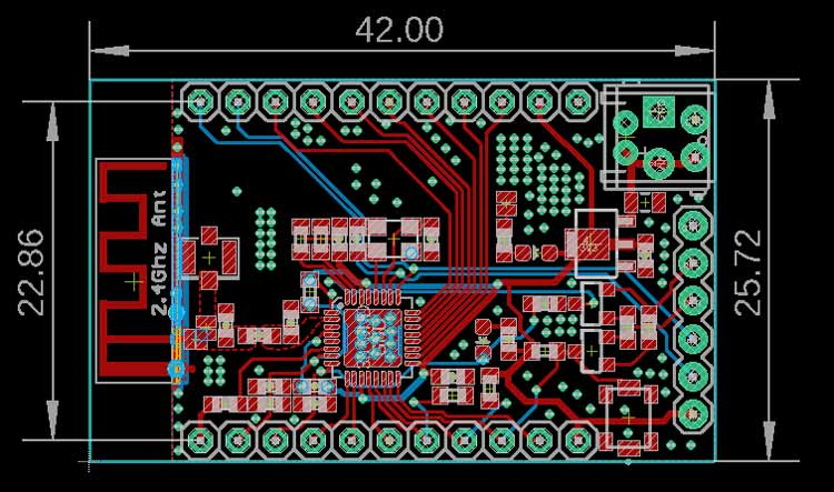
The client required 200 PCB prototypes 4-layer FR4 0.8mm thickness with impedance control 50Ω compatibility with medical-grade components and compliance with Pakistan’s medical device regulations. They needed prototypes delivered within 5 business days to meet product testing timelines with a minimum yield rate of 98%.
Project Challenges
The design required 0.3mm tight component spacing and precise impedance control which local providers could not consistently achieve. The client needed free DFM analysis to fix design flaws real-time production tracking for on-time delivery and PCB prototypes compliant with ISO 13485 standards for Pakistan’s medical device registration.
Our Solutions
We conducted free DFM analysis identifying 3 design flaws component spacing and impedance mismatches and provided adjustments for manufacturability. We used advanced drilling and printing equipment to achieve 0.3mm component spacing and precise impedance control. Our MES system provided real-time production tracking and we prioritized the order to meet the 5-day deadline using our 24-hour production capacity for critical stages.
Output Results
We delivered 200 PCB prototypes in4.5 business days exceeding the client’s timeline. The prototypes achieved a 99.5% yield rate with zero electrical or structural defects. Client testing confirmed prototypes met all medical device specifications and ISO 13485 standards. Post-project feedback noted “EBest’s PCB prototyping service eliminated our delivery and quality concerns allowing us to launch our product on schedule their attention to detail and transparency were unmatched.”
FAQs About PCB Prototyping in Pakistan
Q1: Can PCB prototypes for medical devices in Pakistan meet ISO 13485 standards?
A1: Yes, EBest’s PCB prototyping services for medical devices in Pakistan fully comply with ISO 13485 standards. We follow strict quality control processes from raw material inspection to final testing and provide documentation to support medical device registration in Pakistan. Our medical PCB prototypes have a 99.5% average yield rate ensuring they meet the rigorous requirements of the medical industry.
Q2: What is the fastest lead time for urgent PCB prototyping in Pakistan?
A2: EBest offers 24-hour fast PCB prototyping service for urgent orders in Pakistan. Our dedicated expedite team prioritizes these orders leveraging advanced production equipment and streamlined workflows to deliver high-quality prototypes within one day. This service is available for all PCB types including flexible rigid and multi-layer prototypes.
Q3: Do I need to order large quantities for PCB prototyping in Pakistan?
A3: No, EBest offers low MOQ with 1 piece minimum order for PCB prototyping in Pakistan. This allows for small-batch orders R&D trials and design testing without excess cost. We maintain the same high quality and attention to detail for all order sizes ensuring even single-piece prototypes meet your specifications.
Q4: How can I ensure my PCB prototype design is manufacturable?
A4: EBest provides free DFM analysis for all PCB prototyping orders in Pakistan. Our team reviews your design to identify potential flaws such as component spacing issues impedance mismatches or manufacturing constraints and provides adjustments to ensure manufacturability. This analysis reduces rework saves time and ensures your prototype meets your design requirements.
Q5: Can I track the production progress of my PCB prototyping order in Pakistan?
A5: Yes, EBest’s MES system allows full production data tracking for PCB prototyping orders in Pakistan. You can monitor every stage of the production process from design review to final delivery in real time. This transparency ensures you stay informed about your order’s progress and can plan accordingly for your project timeline.
Choose EBest for Your PCB Prototyping in Pakistan Needs
Are you ready to start your project? Don’t let delayed prototypes or inconsistent quality slow down your product launch. EBest’s PCB prototyping in Pakistan is built for speed, precision, and peace of mind, whether you need a 24-hour urgent prototype or a full production run, we’ve got you covered. Contact us now to get a quote for your project: sales@bestpcbs.com.