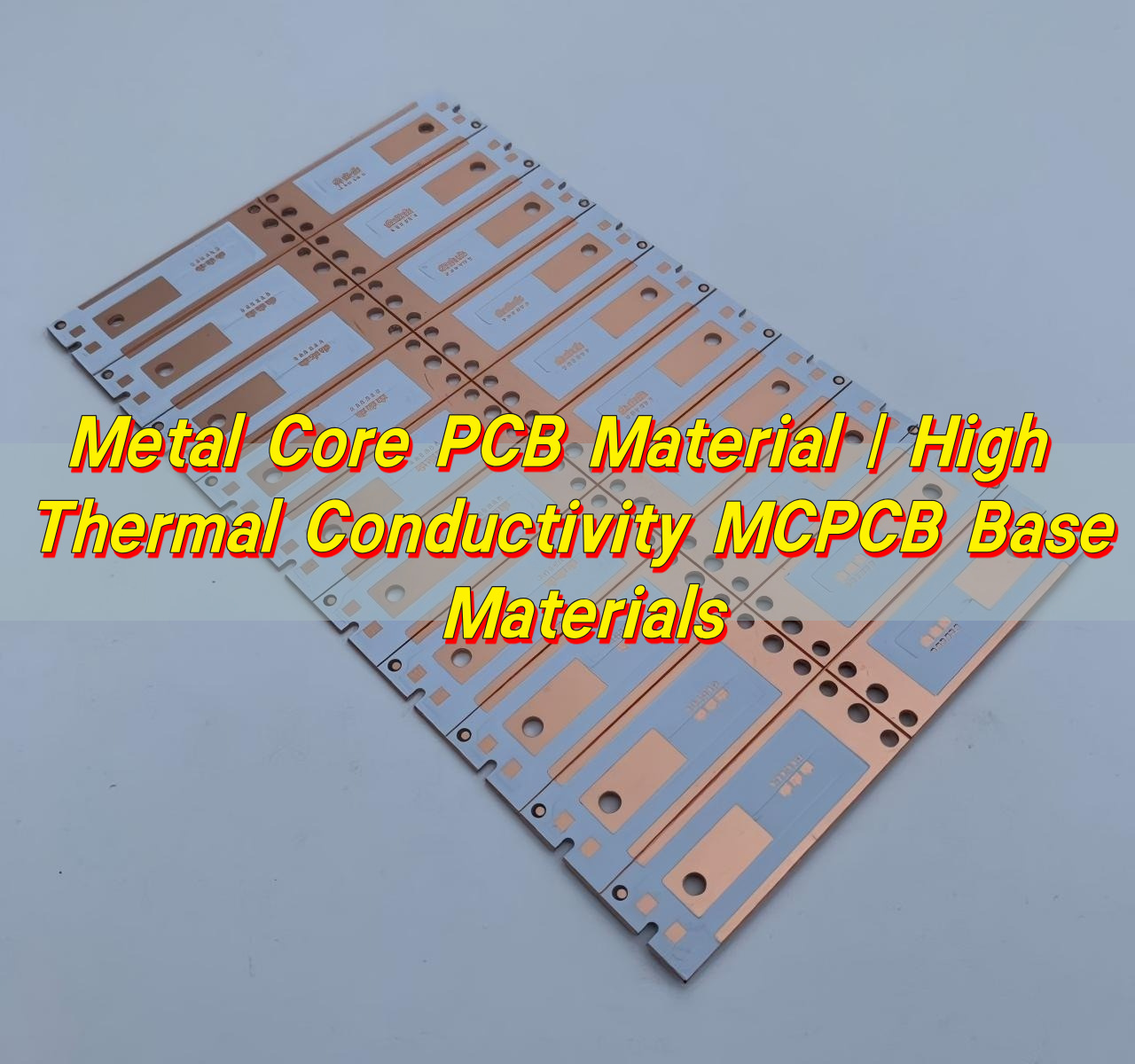
Many electronic products now run hotter, smaller, and faster than before. That shift makes thermal design more important than ever. In many cases, standard FR4 works well. But when heat becomes harder to manage, ceramic substrates offer a more dependable path. With thermal conductivity that can reach 20 to 30 W/m·K for alumina and around 170 to 200 W/m·K for aluminum nitride, ceramic materials are often selected for power modules, LED lighting, RF products, and automotive electronics.
n this guide, you will learn what ceramic PCB design means, which materials are commonly used, how ceramic boards are manufactured, and how to choose between ceramic PCB and FR4 for different applications.
What Is Ceramic PCB Design?
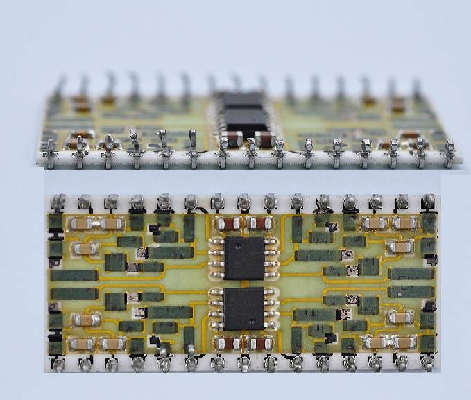
Ceramic PCB design refers to the process of creating a printed circuit board on a ceramic substrate instead of a traditional FR4 base. In this type of board, the substrate does more than support the circuit. It also helps with heat transfer, insulation, and structural stability.
That is why ceramic PCB design is often used in applications where thermal control matters. A well-designed ceramic board can help reduce hot spots, support stable electrical performance, and improve product life in compact or high-power environments.
Typical application areas include:
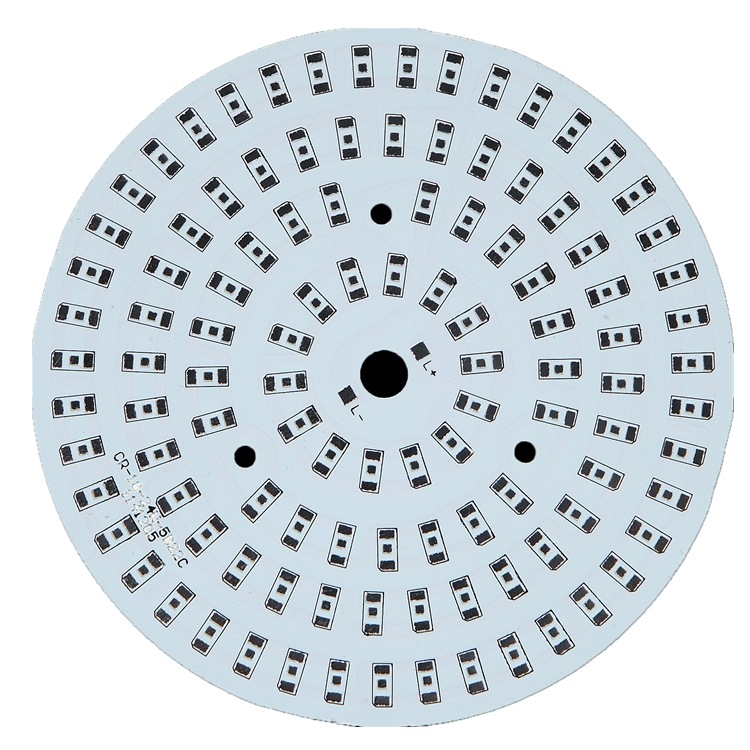
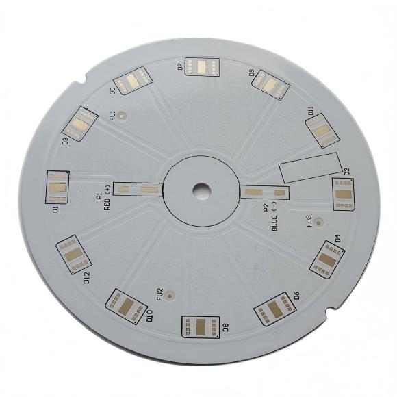
- High-power LED modules
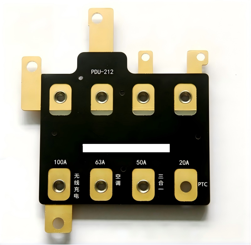
- Power semiconductor circuits
- RF and microwave products
- Automotive control systems
- Medical and industrial electronics
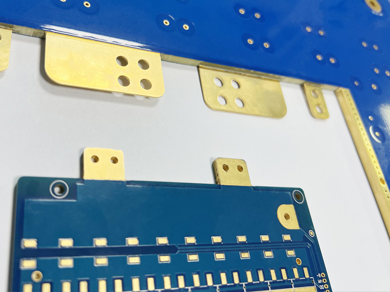
Ceramic PCB Design
Why Choose Ceramic PCBs?
Ceramic PCBs are widely used because they combine heat dissipation and electrical insulation in one structure. This can make the full product design more efficient, especially in space-limited applications. Main advantages include:
- Better heat dissipation than standard FR4
- Stable performance under temperature cycling
- Strong electrical insulation
- Good dimensional stability
- Suitable for compact and high-density layouts
For many engineers, the main attraction is thermal performance. Standard FR4 is usually around 0.3 W/m·K, which is enough for many general products. But for higher heat loads, ceramic substrates offer a clear improvement.
Why Choose Ceramic PCBs?
Common Materials Used in Ceramic PCB Design
Choosing the right ceramic pcb material is one of the first decisions in the design process. Different materials offer different thermal and mechanical properties.
| Material | Thermal Conductivity | Cost Level | Typical Use |
| Al2O3 | 20–30 W/m·K | Lower | LED, sensors, control boards |
| AlN | 170–200 W/m·K | Higher | Power modules, RF, high-heat products |
| Si3N4 | 70–90 W/m·K | Higher | High-reliability power electronics |
| BeO | Very high | High | Special industrial applications |
In most commercial projects, the main decision is between Al2O3 and AlN.
Al2O3 vs AlN: Which One Is Suitable for Your Ceramic PCB Project?
Both materials are common in ceramic PCB design, but they fit different needs.
| Property | Al2O3 | AlN |
| Cost | More economical | Higher |
| Thermal Conductivity | Moderate | Very high |
| Availability | Broad | More specialized |
| Best For | General ceramic circuits | High-power thermal applications |
A simple selection logic is:
- Choose Al2O3 when you need a practical ceramic solution with balanced cost and performance.
- Choose AlN when your board must remove heat faster or work in a tighter thermal environment.
- Review the total thermal path before making the final decision.
If the product is compact, sealed, or power-dense, AlN often provides more design margin. If the thermal load is moderate, Al2O3 is often the more economical choice.
Ceramic PCB vs FR4 PCB: What’s the Difference?
The discussion around ceramic pcb vs fr4 is common because both materials serve important roles.
| Aspect | Ceramic PCB | FR4 PCB |
| Thermal Conductivity | Higher | Lower |
| Heat Resistance | Better | Moderate |
| Dimensional Stability | Strong | Standard |
| Mechanical Nature | Harder, more brittle | Tougher, more flexible |
| Cost | Higher | Lower |
| Typical Use | Power, RF, LED | General electronics |
In short:
- FR4 is suitable for standard and cost-sensitive electronics.
- Ceramic PCB is more suitable for high-heat and high-reliability designs.
So the real question is not which one is better overall, it based on which one fits your product conditions better.
Ceramic PCB Design Guidelines
Ceramic PCB design is not simply FR4 layout on a different substrate. The material behaves differently in thermal transfer, mechanical strength, copper bonding, and assembly response. If these factors are considered early, the board is easier to manufacture and more stable in use.
1. Start with thermal goals, not only electrical layout
Most ceramic PCB projects begin because heat is already a concern. So the design should first identify where the heat is generated, how much power is lost, and where that heat will go next.
A practical design review usually includes:
- heat source location
- power density of major components
- thermal path from device to substrate
- interface to heat sink or housing
- operating ambient temperature
For example, if a board carries LED chips, power ICs, or RF devices, placing those parts without a clear heat path can waste the thermal advantage of the ceramic substrate.
2. Choose the right ceramic material for the real operating condition
Material selection affects the whole design window. Al2O3 is widely used because it offers good insulation, mature processing, and reasonable cost. AlN is better when the thermal load is higher and the product has less room for heat buildup.
This choice should match the actual project target, not only the material data sheet. A low-power control board and a compact power module should not use the same logic.
3. Match copper layout with current, heat, and process capability
Copper traces on ceramic boards should be designed with three things in mind:
- current carrying ability
- heat spreading
- manufacturability
Very narrow traces may look efficient in layout, but they are not always ideal for yield or long-term reliability. Wider copper areas can help thermal spreading, but overly large copper imbalance may create stress during heating and cooling cycles.
4. Pay close attention to pad design and solder joint reliability
Pad design matters more than many designers expect. Ceramic substrates are rigid, and the expansion behavior differs from FR4. That means poor pad design can affect solder joint stability, especially in power devices or larger packages.
It is wise to check:
- pad size versus component package
- solder fillet space
- thermal pad design
- copper symmetry around large pads
- assembly method and reflow profile
This is especially important for LED chips, bare die, power packages, and ceramic-mounted RF parts.
5. Consider brittleness in the mechanical design
Ceramic offers excellent stability, but it is also more brittle than FR4. That means the board design should avoid stress concentration.
Important mechanical points include:
- leave enough clearance from holes to edges
- avoid weak narrow bridges in the outline
- reduce sharp internal corners where possible
- design mounting areas with even force distribution
- avoid layout features too close to cut edges
In short, ceramic PCB design should not only perform well electrically. It should also survive handling, assembly, fastening, and real product use.
6. Align the design with the selected manufacturing process
This point is often overlooked. Ceramic PCB design should always match the actual process route. If the board will be made by DPC ceramic PCB technology, then line width, spacing, via structure, copper thickness, and surface finish should all follow DPC process capability.
That is why early communication with the manufacturer is valuable. A design that fits the real process window usually moves to production faster and with fewer revisions.
Ceramic PCB Manufacturing Processes
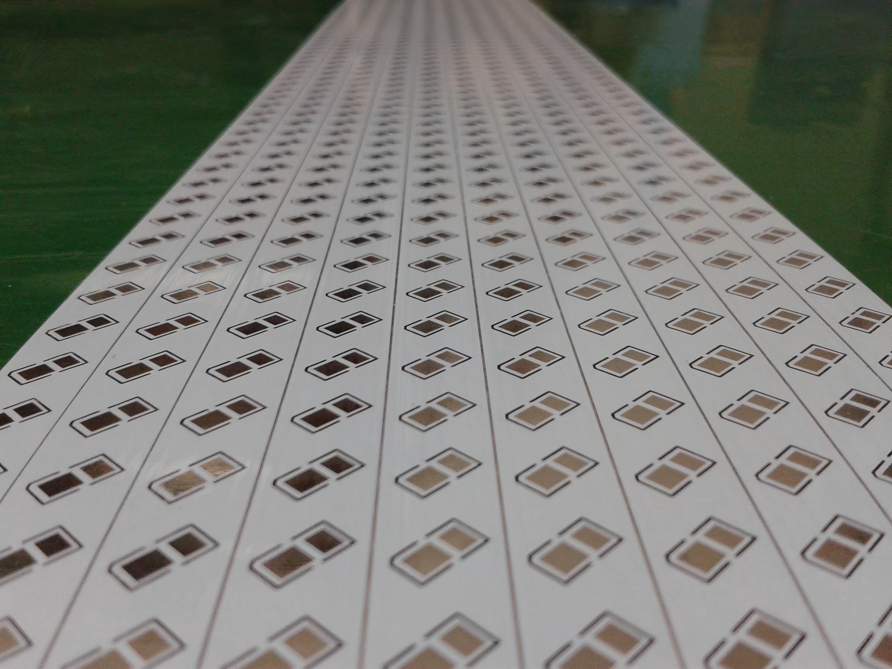
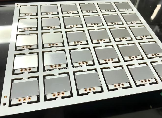
There are several ceramic PCB manufacturing methods, but for projects that require fine lines, good adhesion, and precise circuit definition, DPC ceramic PCB is a widely used option. DPC stands for Direct Plated Copper. This process forms the copper circuit directly on the ceramic substrate through thin film metallization and copper plating steps.
Compared with thick film processes, DPC is often preferred for finer circuit patterns and more controlled conductor formation. It is commonly used in LED packaging, RF modules, sensors, and high-precision ceramic circuit applications.
DPC Ceramic PCB Manufacturing Flow
Here is the typical DPC ceramic PCB manufacturing process:
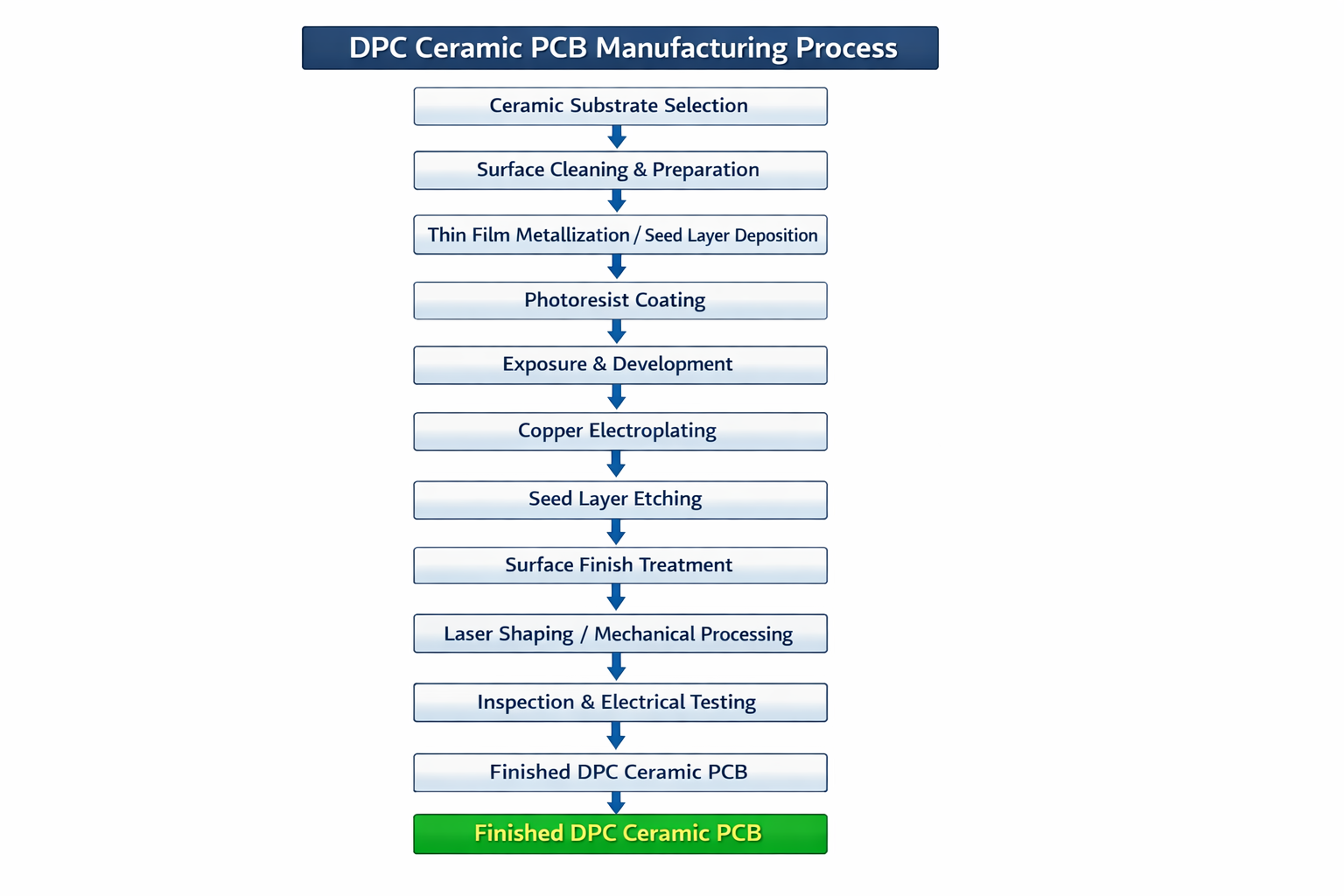
1. Ceramic substrate preparation
The process begins with the selected ceramic substrate, usually Al2O3 or AlN. The surface must be cleaned carefully to remove particles, oil, and contamination. This step is important because good surface condition helps the following metal layer bond more reliably.
2. Thin film metallization
A thin metal seed layer is deposited on the ceramic surface. This layer often includes metals such as titanium, copper, or other adhesion and conductive layers depending on the process design. Its role is to provide a base for later copper plating.
3. Photoresist coating
A photoresist layer is applied to the metallized ceramic surface. This creates the imageable layer used to define the circuit pattern.
4. Exposure and development
The circuit image is transferred onto the photoresist by exposure. After development, the required copper pattern area is opened, while the rest remains protected.
5. Copper electroplating
Copper is plated onto the exposed circuit areas until the target thickness is reached. This step builds the actual conductive traces and pads. The plating thickness is controlled based on current requirement, pattern accuracy, and product application.
6. Resist stripping
After plating is completed, the remaining photoresist is removed. At this stage, the plated copper pattern remains on the substrate.
7. Seed layer etching
The exposed thin seed layer that is no longer needed is etched away. This leaves only the final circuit pattern on the ceramic substrate.
8. Surface finish treatment
A suitable surface finish is applied to improve solderability, bonding performance, or corrosion resistance. Common finishes depend on the product design and assembly method.
9. Laser drilling or shaping if needed
If the design requires slots, openings, or special board outlines, laser or precision machining processes are used. Ceramic substrates need careful shaping because the material is hard and brittle.
10. Final inspection and testing
The finished board goes through dimensional inspection, circuit inspection, adhesion testing, and appearance review. For higher-end applications, extra checks may include thermal cycling, insulation performance, and bonding quality verification.
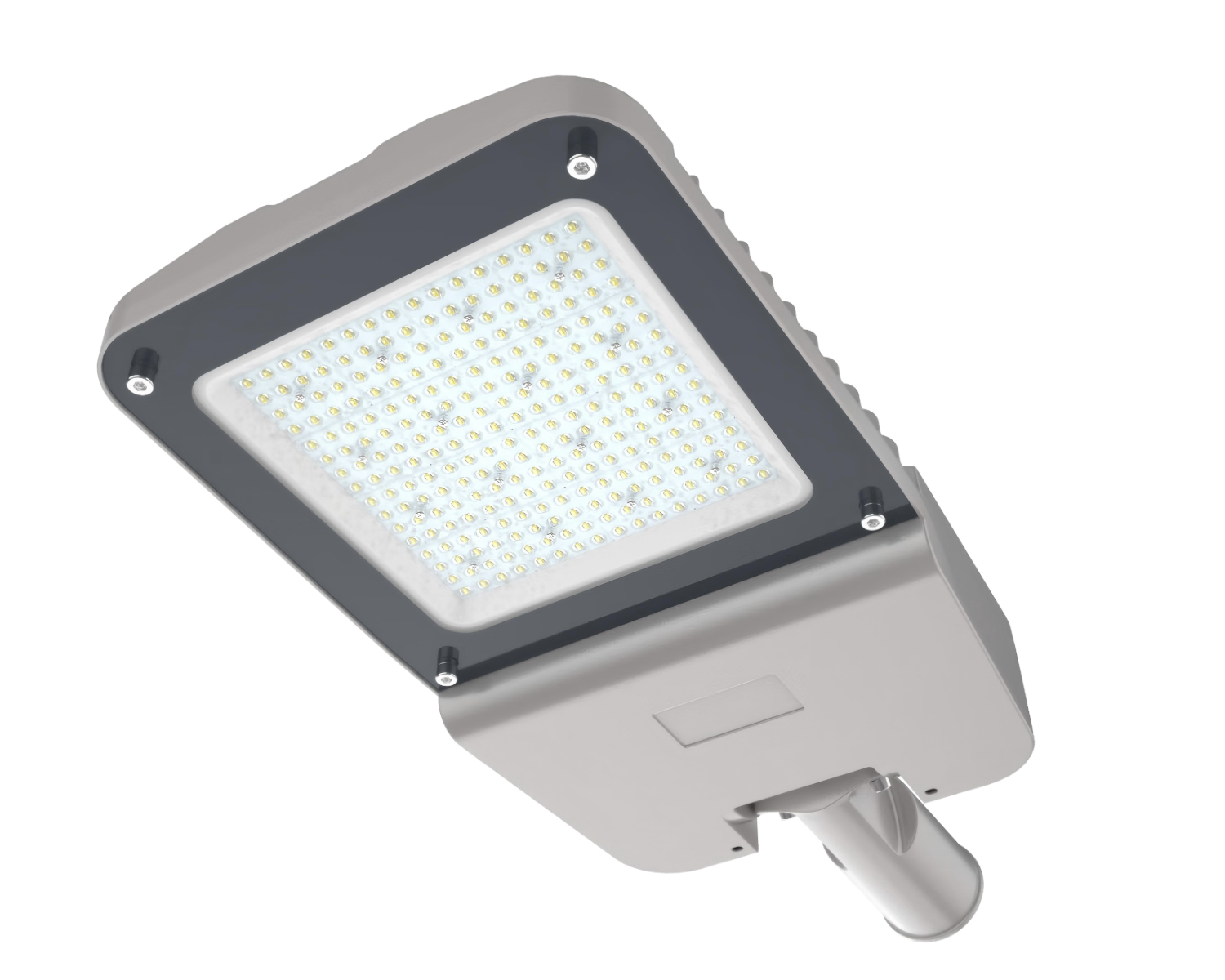
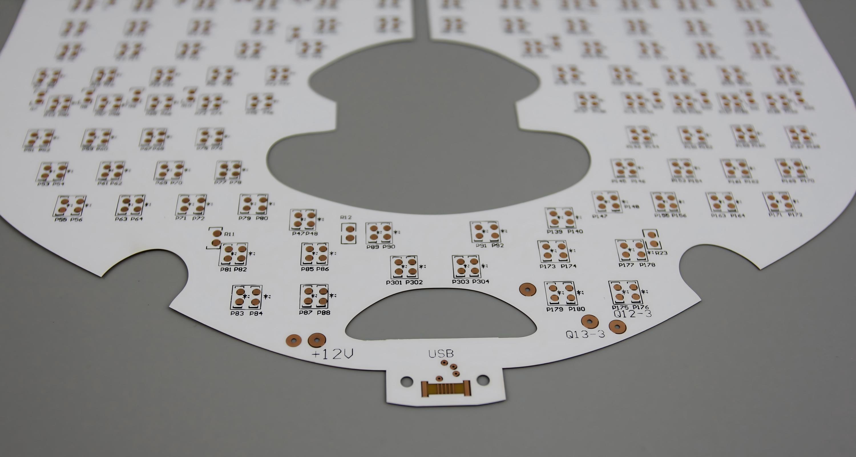
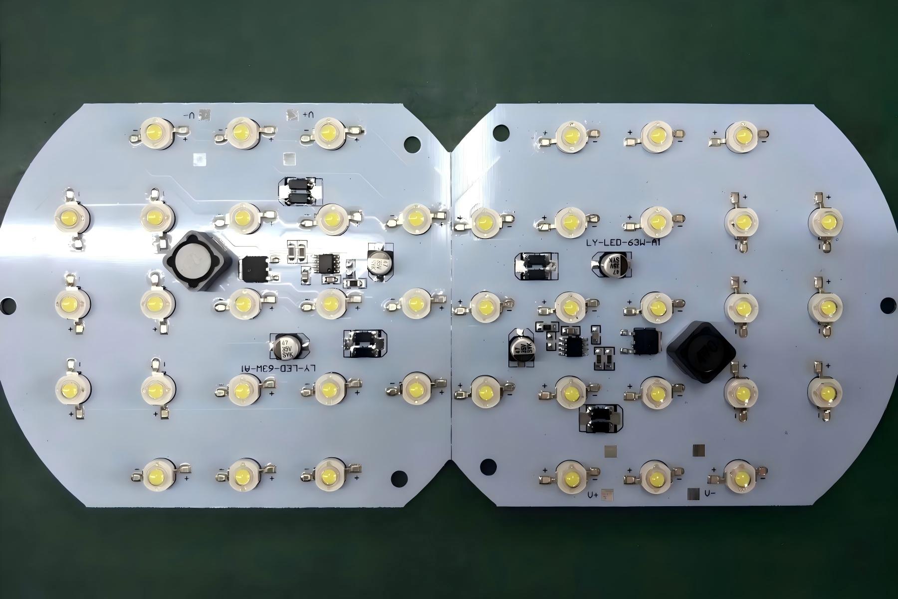
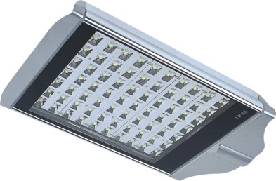
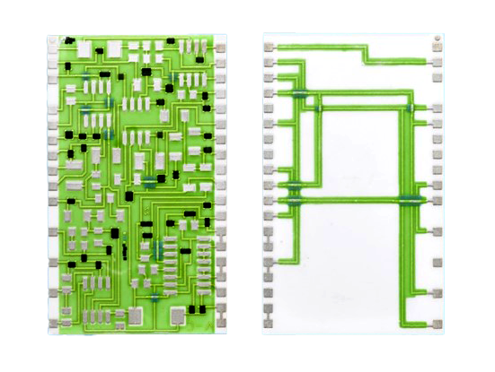
Applications of Ceramic PCB Design
Ceramic PCB design is widely used in products that need strong thermal performance and stable operation over time.
Common applications include:
- LED lighting modules
- Automotive electronics
- Power control systems
- RF and microwave devices
- Medical equipment
- Industrial power modules
- Laser and communication products
In high-power LED systems, ceramic substrates help transfer heat away from the LED source. In automotive and industrial electronics, they support more stable operation under repeated thermal cycling.
Applications of Ceramic PCB Design
Why Choose EBest Circuit for Ceramic PCB Design?
With 20+ years of PCB and PCBA experience, EBest Circuit supports customers from early design review to full production. We have served 10,000+ engineers and 1,800+ customers, giving us broad experience across thermal management, high-reliability electronics, and complex PCB structures.
Why many customers choose EBest Circuit for ceramic PCB design:
- 20+ years of manufacturing experience in PCB and PCBA
- Support for advanced materials, including Al2O3 ceramic PCB and AlN ceramic PCB
- Engineering-driven support with free DFM review and process suggestions
- One-stop capability from PCB fabrication to PCBA assembly and testing
- Fast response for prototype and small-batch projects
- Quality systems supported by ISO 9001, ISO 13485, IATF 16949, and AS9100D
- MES-based traceability for better process control and production visibility
We also understand that ceramic PCB projects are often tied to demanding applications such as LED lighting, power electronics, RF devices, and industrial controls. In these products, stable quality and process consistency are just as important as thermal performance on paper. That is why we focus on both engineering review and manufacturing control.
If you need a ceramic PCB manufacturer that can support design optimization, material selection, and reliable production, EBest Circuit is ready to help. For project discussion or quotation, please contact sales@bestpcbs.com.
FAQs About Ceramic PCB Design
1. What is ceramic PCB design used for?
Ceramic PCB design is used for electronic products that need better heat dissipation, strong insulation, and stable operation in demanding environments.
2. Which ceramic pcb material is most common?
Al2O3 is one of the most common materials because it offers a good balance of cost and performance.
3. When should I choose AlN?
AlN is a better choice when the design has high heat density or requires faster heat transfer.
4. Is ceramic PCB better than FR4?
For thermal-intensive applications, ceramic is usually a better option. For standard electronics, FR4 is often enough.
5. Can a ceramic pcb manufacturer help optimize my design?
Yes. Early design review can improve manufacturability, reduce risk, and shorten project cycles.
6. Are ceramic PCBs suitable for LED products?
Yes. They are widely used in high-power LED modules because heat dissipation is critical.