In today’s era of rapid technological development, ceramic PCBs have emerged in many fields with their excellent performance and unique advantages. Behind ceramic PCBs are a group of professional ceramic PCB manufacturers who are promoting the progress and development of the electronics industry with their unremitting efforts and superb skills.
Reasons for the development of ceramic pcb manufacturer
- (I) Expansion of market size
In recent years, the ceramic PCB market size has shown a growing trend. According to statistics, the global ceramic substrate market size reached US$1.13 billion in 2022 and is expected to reach US$4.15 billion in 2029, with a compound annual growth rate (CAGR) of 18.23%.
In the Chinese market, the market size of China’s ceramic circuit board industry is about 2.399 billion yuan by 2023, with a CAGR of 19.1% from 2015 to 2023.
In terms of output, China’s ceramic substrate output accounted for about 35.9% of the world’s total in 2022, and is expected to reach 54.9% in 2029. Europe is the second largest market region, with a share of 33% in 2022 and an estimated 21.99% in 2029. Japan, Southeast Asia, South Korea and Taiwan are also important production areas.
- (II) Promotion of technological progress
Technological innovation plays a vital role in promoting ceramic PCB manufacturers. In terms of the application of new materials, the research and development of new ceramic materials provides more options for ceramic PCBs.
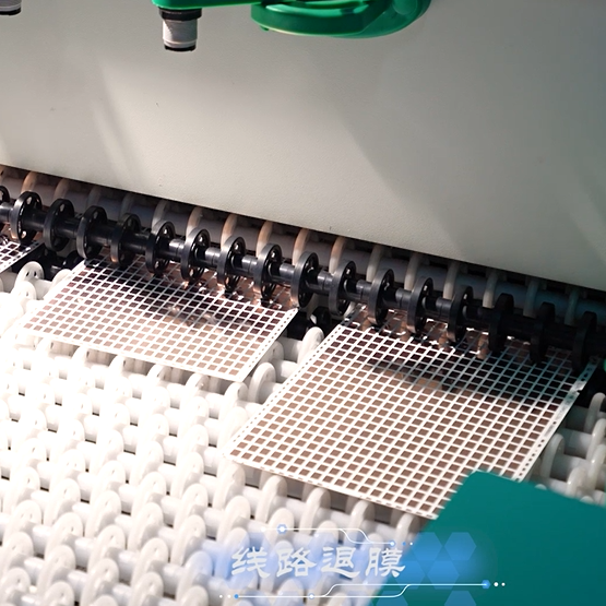
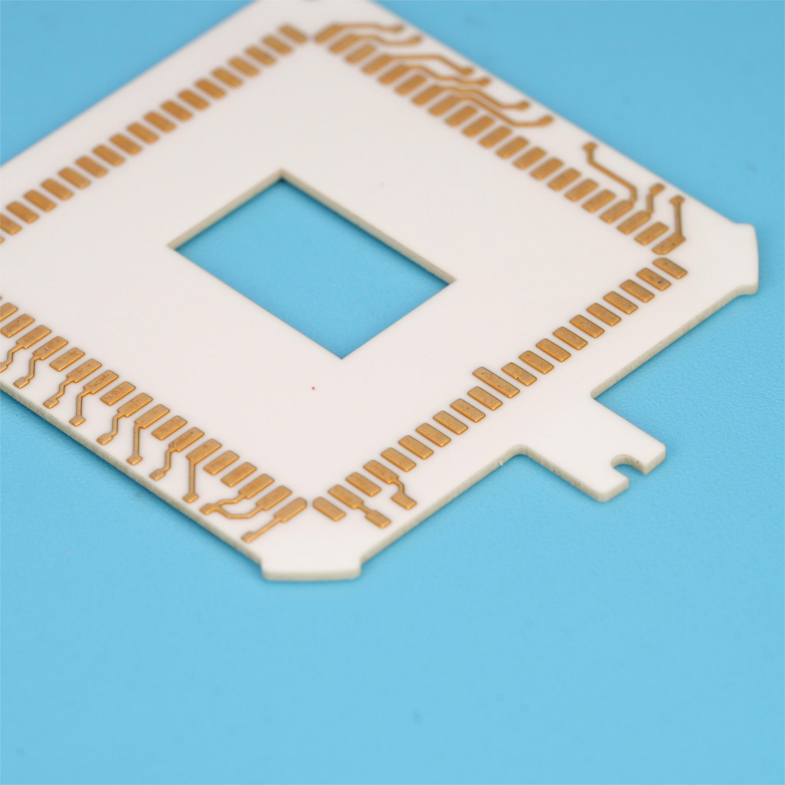
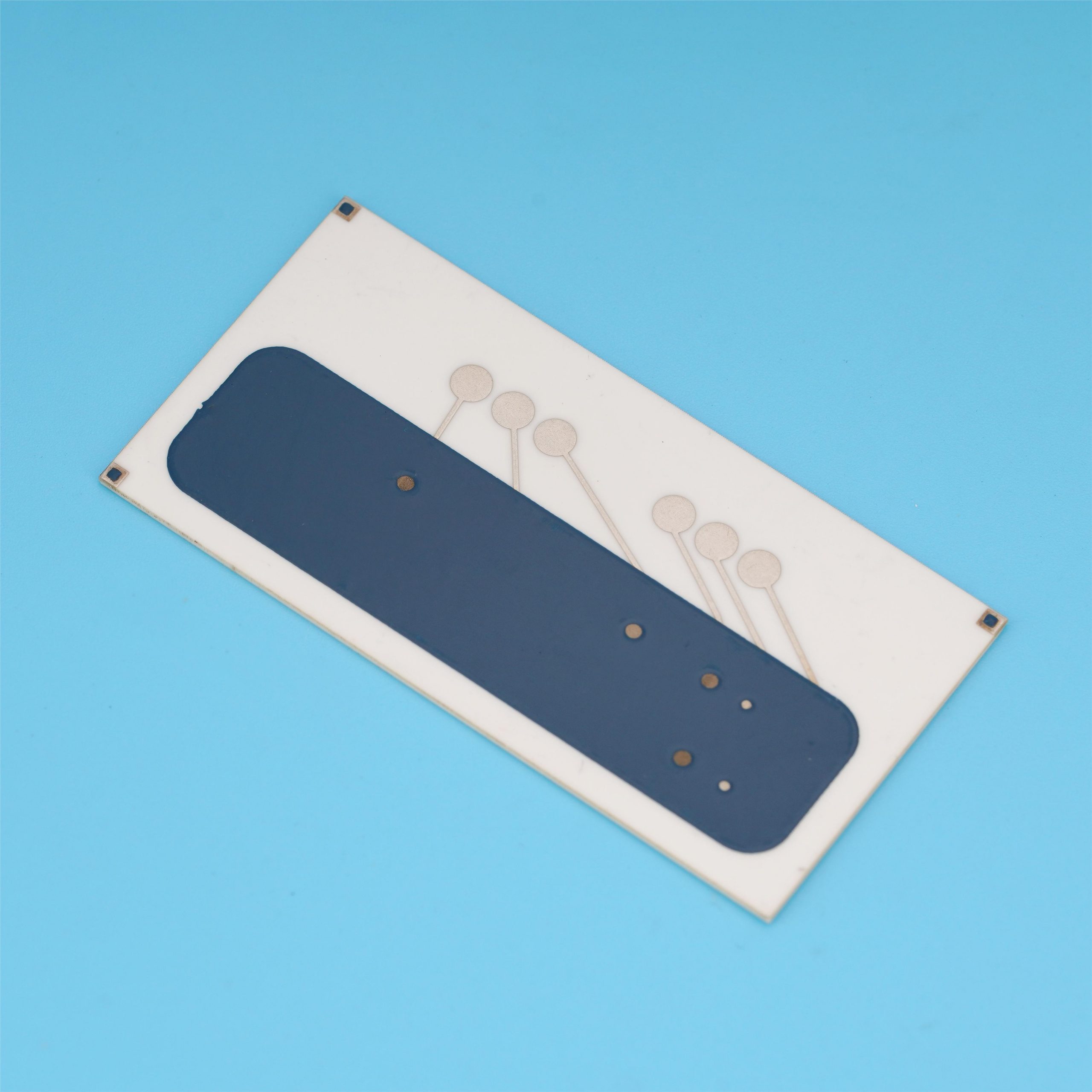
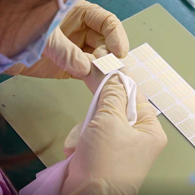
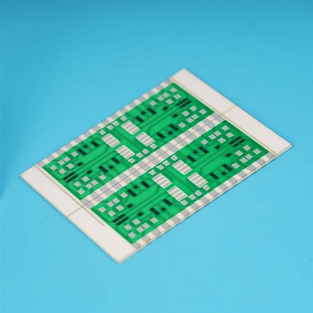
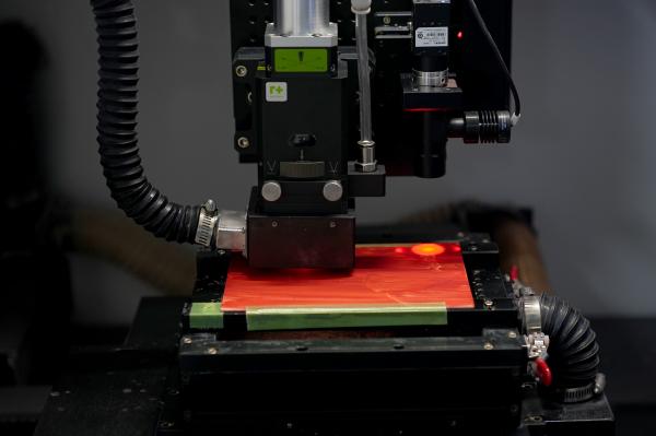
In terms of production process improvements, ceramic PCB manufacturing technology includes steps such as pressing, welding, metallization and printing. By optimizing process parameters and process control, higher quality ceramic PCBs can be obtained.
The application of laser cutting and punching technology in the production of ceramic circuit boards improves processing accuracy and speed, and meets the requirements of small size and high density of electronic devices and semiconductor components.
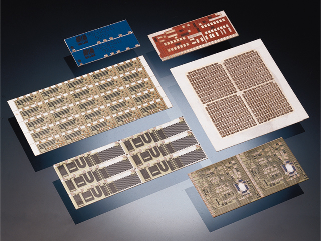
What are the well-known ceramic pcb manufacturers?
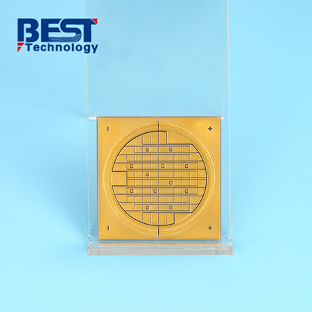
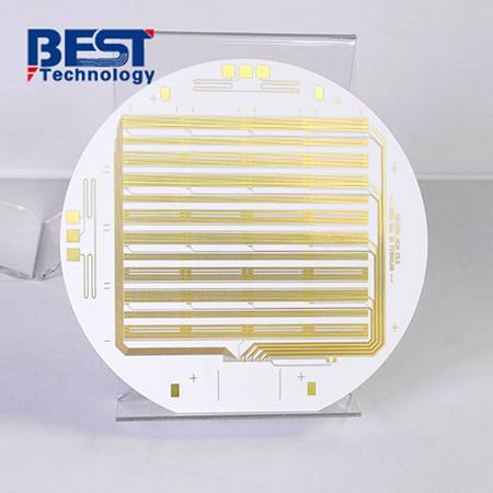
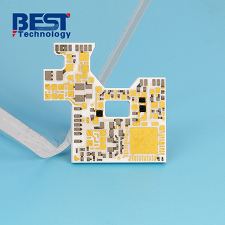
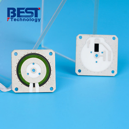
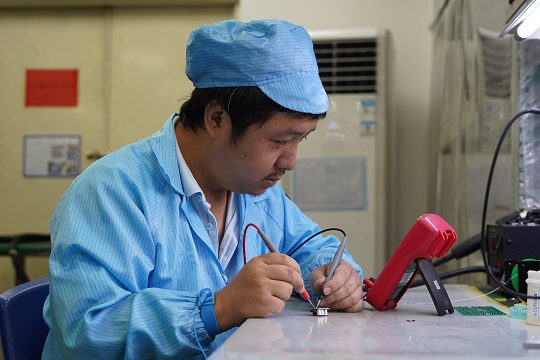
BEST Technology:
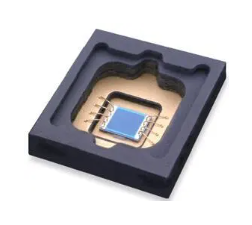
- Product features: A domestic manufacturer that focuses on the R&D and production of large, medium and small batches of ceramic circuit boards and prototypes, serving high-tech enterprises and scientific research institutions at home and abroad. Mainly focused on MCPCB, FR4 PCB, Ceramic PCB, Special PCB such as Heavy Copper (up to 20 OZ), and PCB assembly service.
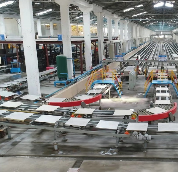
- Market share: Ranked among the top domestic ceramic substrate manufacturers, with a monthly production capacity of 100,000 sheets.
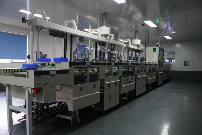
- Technical advantages: Over 18 years of experience in the PCB industry. Proficient in DPC, AMB, DBC, LTCC, HTCC production processes, fully passed TS16949, ISO9001, ISO14001 certification. With the aim of “zero quality defects”, we provide high-quality products and services, with short delivery time and stable quality for ceramic boards.
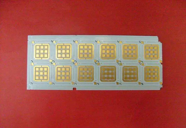
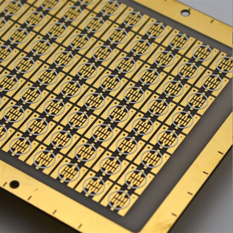
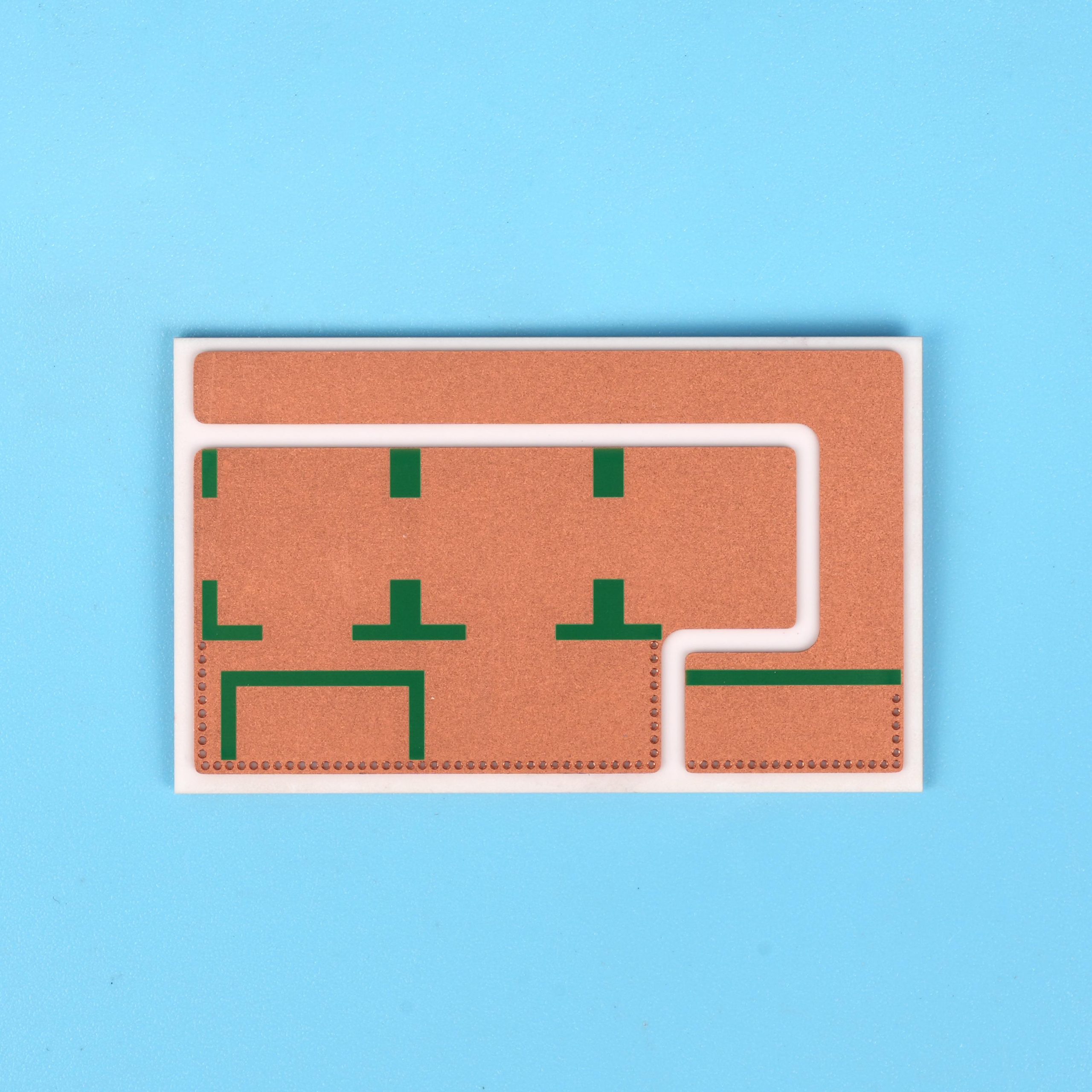
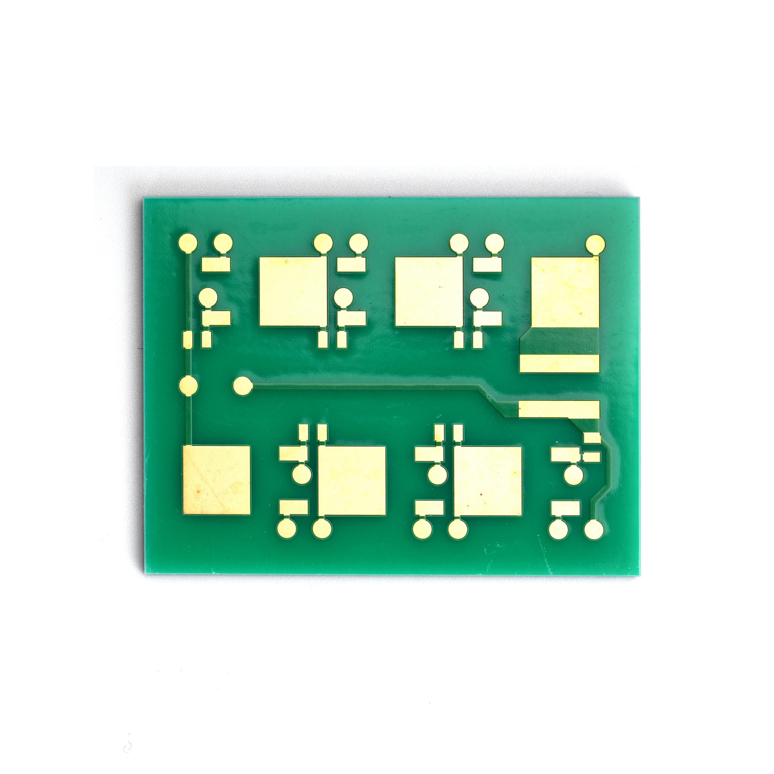
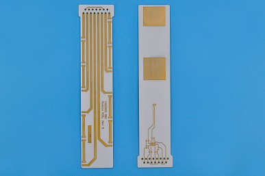
What are the production processes of ceramic PCBs?
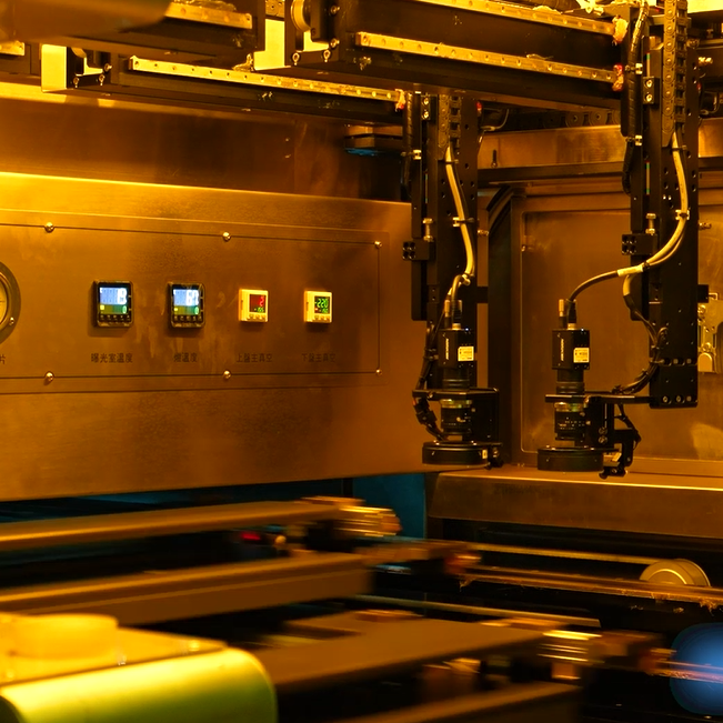
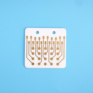
(I) Laser processing technology
Lasers play a vital role in ceramic PCB processing. Laser drilling has the advantages of high precision and high efficiency, and can meet the requirements of electronic devices and semiconductor components for micropore diameters ranging from 0.05 to 0.2 mm.
Laser cutting also has many advantages. First, it has high precision, fast speed, narrow slits, small heat-affected zone, and smooth cut surfaces without burrs.
(II) Other molding processes
- Tape casting: The advantage is that it can produce large-area, thin-thickness and uniform ceramic substrates, which are suitable for large-scale production. However, tape casting has high requirements for equipment, and the viscosity and fluidity of the slurry need to be controlled during the process.
- Powder pressing: Simple operation and low cost. However, the pressed ceramic substrate may have problems of uneven density and high porosity, which affect its performance.
- Extrusion molding: Suitable for the production of long strip or tubular ceramic substrates with high production efficiency. However, the shape of the extruded ceramic substrate is relatively simple and the dimensional accuracy is relatively low.
(III) LAM process advantages
The LAM process has significant advantages in ceramic PCB manufacturing.
First, the bonding strength between the metal layer and the ceramic is high, up to 45 MPa (the strength of the ceramic sheet is greater than 1mm thick), the conductivity is good, and the heat is small when the current passes through.
Secondly, the thermal conductivity is high. The thermal conductivity of alumina ceramics is 20-35 W/mk, and the thermal conductivity of aluminum nitride ceramics is 170-230 W/mk, which is much higher than the thermal conductivity of the traditional aluminum-based circuit board MCPCB of 1 to 2 W/mk.
In addition, the insulation is good, and the breakdown voltage is as high as 20KV/mm. The thickness of the conductive layer can be customized arbitrarily within the range of 1μm-1mm, and the current can be designed according to the circuit module. The thicker the copper layer, the greater the current passing through.
The high-frequency loss is small, and high-frequency circuits can be designed and assembled; the dielectric constant is very small, and the line/spacing (L/S) resolution can reach 20μm, thus achieving short and thin devices.
It does not contain organic components, is resistant to cosmic rays, and has high reliability and long service life in the aerospace field; the copper layer does not contain an oxide layer and can be used for a long time in a reducing atmosphere.
What are the characteristics of ceramic pcb manufacturer?
- (I) Obvious technical advantages
Ceramic PCB manufacturers have significant technical advantages. First of all, high thermal conductivity is one of the outstanding features of ceramic PCB. This enables ceramic PCB to effectively dissipate heat in high-power electronic equipment and improve the reliability and stability of the equipment.
Low thermal expansion coefficient is also an important technical feature of ceramic PCB. Its thermal expansion coefficient is close to that of silicon chips, which can save labor and materials and reduce costs. At the same time, when the temperature changes, it can reduce the stress caused by thermal expansion and contraction, and ensure the stability of the circuit.
High surface hardness makes ceramic PCB more durable and longer service life. Compared with traditional PCBs, ceramic PCBs are not easily scratched and worn, and can maintain good performance in harsh environments.
- (II) Adapt to a variety of fields
Ceramic PCB has a wide range of application advantages in many fields.
In the field of LED lighting, the excellent heat dissipation performance of ceramic PCB can effectively reduce the temperature of LED chips, improve luminous efficiency and life. At the same time, ceramic PCB has good insulation and high pressure resistance, which ensures personal safety and equipment protection.
In the semiconductor field, the high thermal conductivity of ceramic PCB can quickly conduct heat away from semiconductor chips and improve cooling efficiency. In addition, the low thermal expansion coefficient and high surface hardness of ceramic PCB can adapt to the working environment of semiconductor coolers at different temperatures and ensure its stable performance.
- (III) Clear market structure
At present, the ceramic PCB market presents a clear competitive pattern. In the global market, a few internationally renowned companies occupy a large market share. These companies have advanced technology and rich experience, and have strong strength in material research and development, production technology and market expansion.
The development opportunities for domestic manufacturers lie in the huge demand and policy support of the domestic market. With the rapid development of strategic emerging industries such as 5G communications, new energy vehicles, and high-end manufacturing, the market demand for ceramic PCBs will continue to grow.
At the same time, domestic manufacturers are also facing some challenges. On the one hand, international competitors have strong technical strength and brand influence, and domestic manufacturers need to increase investment in technological innovation and brand building. On the other hand, the production cost of ceramic PCBs is high, and domestic manufacturers need to continuously optimize production processes, reduce costs, and improve the cost performance of products.
What is the market prospect of ceramic PCB manufacturers?
(I) Strong policy support
As the core material of passive electronic components, electronic ceramics are an important material basis for electronic information technology.
In order to promote the development of the electronic ceramics industry, the state has issued a series of policies, such as “Opinions on Deepening the Reform of the Management System of the Electronic and Electrical Industry”, “The 14th Five-Year Plan for the Development of the Digital Economy”, “The 14th Five-Year Plan for the Development of Intelligent Manufacturing”, and “The 14th Five-Year Plan for the Development of China’s Electronic Components Industry”.
At the same time, the state has also strengthened quality management supervision of the PCB board industry, formulated strict quality standards and testing requirements, and supported enterprises to carry out ISO quality management system certification to improve product quality and competitiveness.
In terms of environmental protection, the Chinese government has adopted strict environmental protection policies to regulate the production and processing processes of the PCB board industry, restrict the use of hazardous substances, promote the recycling of resources and promote clean production, laying a solid policy foundation for the development of ceramic PCB manufacturers.
(II) Market demand growth
With the rapid development of downstream application fields such as new energy vehicles and 5G communications, the market demand for ceramic PCBs has shown a strong growth trend.
In the field of new energy vehicles, a large number of high-voltage and high-power devices contained in new energy vehicles, such as IGBT and MOSFET, have high requirements for heat dissipation.
Ceramic substrates have a good heat dissipation effect, which can dissipate the high heat in the power system in time to ensure the normal operation of large power loads, further increasing the use of PCBs for new energy vehicles.
In the field of 5G communications, the advent of the 5G era has made signal base stations more dense, with the number reaching 100 times that of 4G, including a series of software and hardware upgrades brought about by the iterative upgrade of terminal receiving devices.
As hardware for high-frequency transmission, the core of it is the circuit board. At present, the circuit board with the smallest transmission loss is the ceramic circuit board, which has long been widely used in the communications industry.
In the future, entering 2020, 5G will be expected to be commercially available. With the development of the new era of 5G, it is expected that by 2030, the domestic direct economic output will reach 6.3 trillion, and 8 million jobs will be created.
(III) Future development trends
- Technological innovation: Ceramic PCB manufacturers will continue to increase their technological innovation efforts, develop new ceramic materials and advanced production processes.
- Product upgrade: With the continuous improvement of PCB performance requirements in downstream application fields, ceramic PCB manufacturers will launch higher-end and more personalized products.
- Market expansion: Ceramic PCB manufacturers will actively expand domestic and foreign markets, strengthen cooperation with downstream customers, and increase the market share of products. In the international market, domestic manufacturers can enhance brand awareness and influence and expand overseas markets by participating in international exhibitions and cooperating with internationally renowned companies.