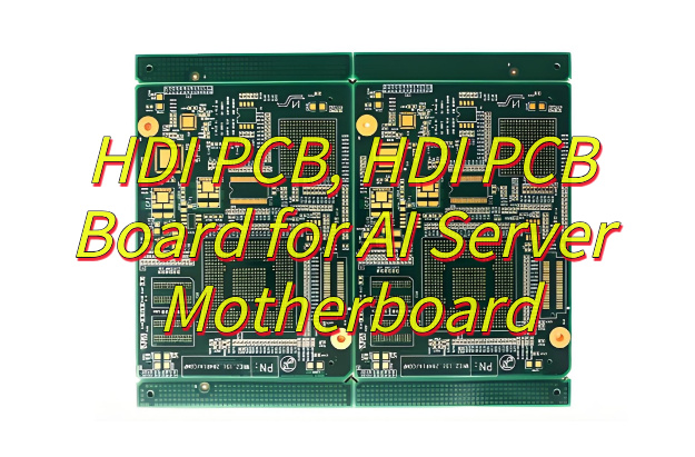
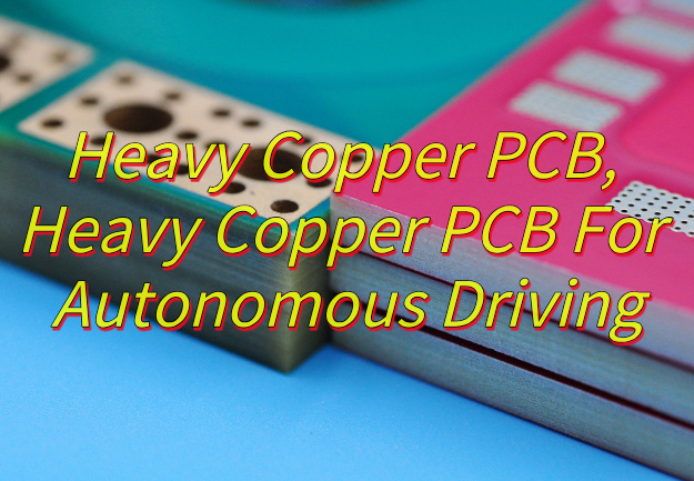
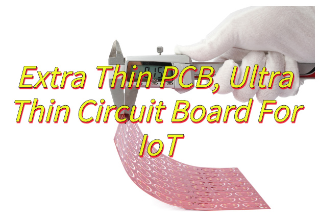
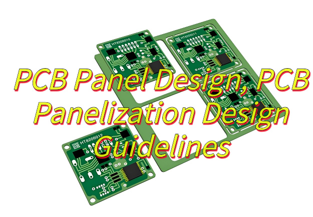
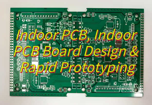
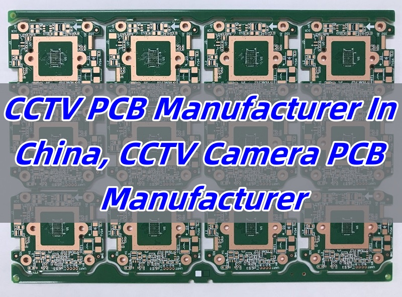
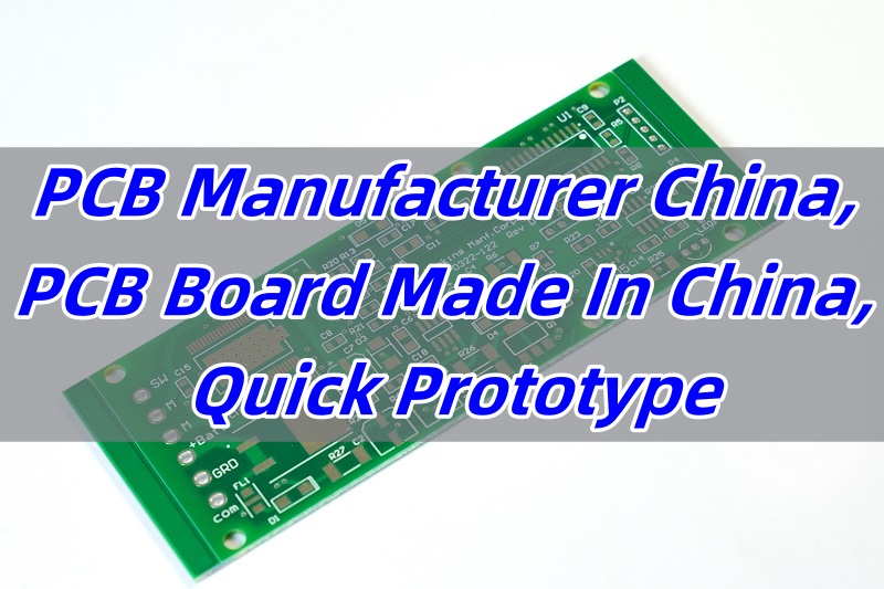
PCB board made in china is a hot topic for engineers who need speed, value, and reliability. This guide uncovers what buyers truly care about when sourcing a PCB board made in China while showing how EBest Circuit (Best Technology) solves customers needs with smart processes and a friendly team.
EBest Circuit (Best Technology) is a PCB Manufacturer China, providing quick prototype, PCB board fabrication, and turnkey assembly services to worldwide clients & markets. As an R&D-driven company, we believe that innovation is paramount for us to get long-term developments. Our company has got some invention patents and utility model patents each year. If you need a PCB Board made in China, just feel free to contact us via sales@bestpcbs.com. We are happy to provide optimum PCB board solutions for your projects.
Which company makes PCB board made in china?
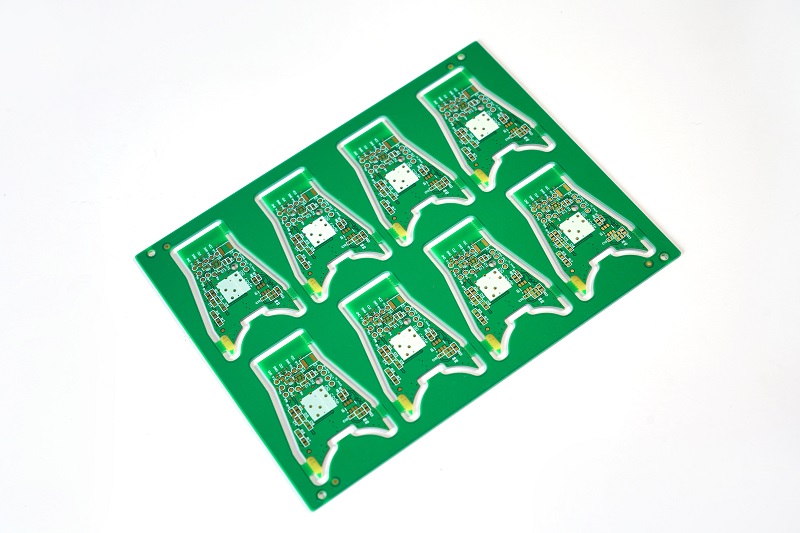
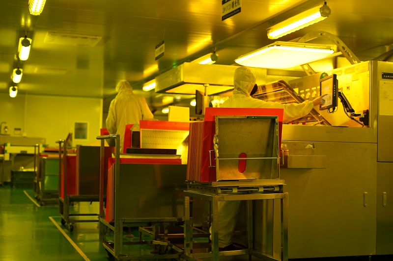
China hosts thousands of board factories, yet only a handful handle complex work with tight control. Names on the top 10 PCB manufacturers in China lists often include large public firms focused on huge volumes. However, mid‑size partners shine when projects vary. EBest Circuit (Best Technology) sits in this sweet spot. We run flexible lines, cover rigid, flex, and ceramic, and keep in‑house assembly under one roof. Our engineers review data up front to avoid shorts, opens, or warpage. That review, plus IPC‑class workmanship, keeps rework low and first‑pass yield high.
Who is the biggest manufacturer of PCB board made in china?
By revenue, the biggest player is a well‑known conglomerate whose plants span multiple provinces. Yet being the largest is not always ideal for quick prototype or small‑batch jobs. Giant lines favor millions of panels. When you need PCB board made in china in ten days, you want focus, not size. EBest Circuit (Best Technology) addresses this need with quick‑change tooling, smart MES, and 3,000 m² of floor space that switches from sample to mass without delay. That flexibility keeps your launch on schedule.
Can I get a quick prototype of a PCB board made in China?
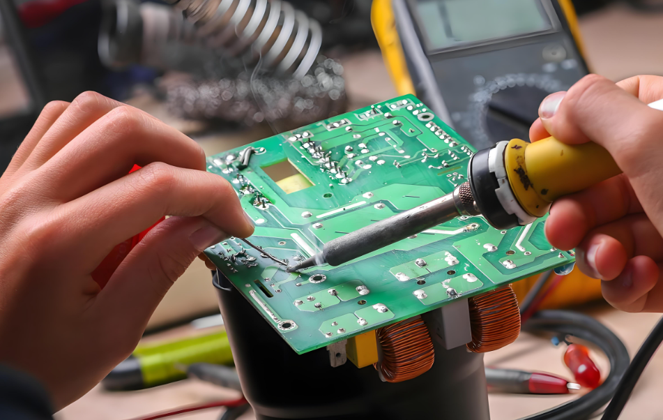
Yes, and it can be faster than local shops thanks to round‑the‑clock production and export hubs near main airports. EBest Circuit (Best Technology) offers a quick prototype service that ships rigid two‑layer samples in 48 hours and complex six‑layer stacks in five days for urgent PCB board projects. We achieve this speed by:
- Keeping core materials like FR‑4, Rogers, and aluminum nitride in stock.
- Running X‑ray drill registration to avoid mis‑hits that would otherwise force remakes.
- Employing courier pickup direct from the plant to cut domestic legs.
With these steps, your first item arrives earlier, giving you more room for design tweaks.
What is the cost of a PCB board made in China for small batches?
Cost depends on layer count, size, finish, and test coverage. For instance, a 100 mm × 100 mm four‑layer board with ENIG finish in ten pieces often lands around USD 80 including SMT stencil. Transparent pricing at EBest Circuit (Best Technology) lists prototype and final electrical assembly separately, so you see value in each line. Because we manage a trusted supplier base for copper foil, raw material swings stay modest. We also offer bundled assembly, saving extra freight legs and cutting total landed cost. That means that your PCB board fabrication and PCB board assembly order will be finished under the same roof at our factory in China. That saves your money, and time and guarantees the PCB board quality.
How long does it take to make a PCB board made in china?
Lead time splits into fabrication and logistics. Standard fabrication times follow:
- Two‑layer: 3‑4 working days.
- Four‑layer: 5‑6 working days.
- Six‑layer and up: 6‑8 working days.
These figures assume full test and IPC‑A‑600 class 2. Add 1‑2 days for ENEPIG or hard gold. Air freight from Shenzhen to the United States usually takes 3‑4 days. Hence, a complete eight‑layer ENIG job can reach your lab in under two weeks.
Where to find manufacturers of PCB board made in China?
You can browse trade fairs, B2B platforms, or industrial clusters like Shenzhen Bao’an or Jiangsu Kunshan. Yet vetting takes time. A faster path is contacting EBest Circuit (Best Technology) directly. Our sales engineers answer in under 12 hours, share DFM feedback, and send a live plant tour video so you see machines, not stock photos. Transparency builds trust and speeds vendor approval on your side.
How to ensure quality when ordering a PCB board made in China?
Success rests on three pillars: design review, process control, and final test.
- Design review. We perform full DFM and impedance checks before drill hits copper. This stops common faults such as solder bridges or acid traps.
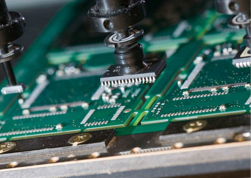
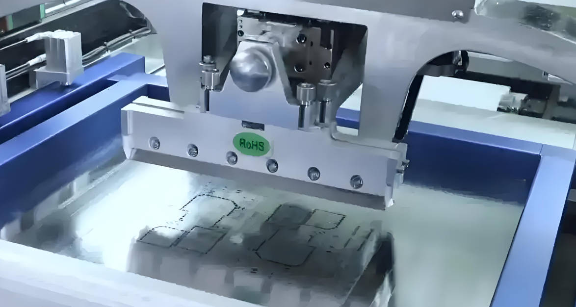
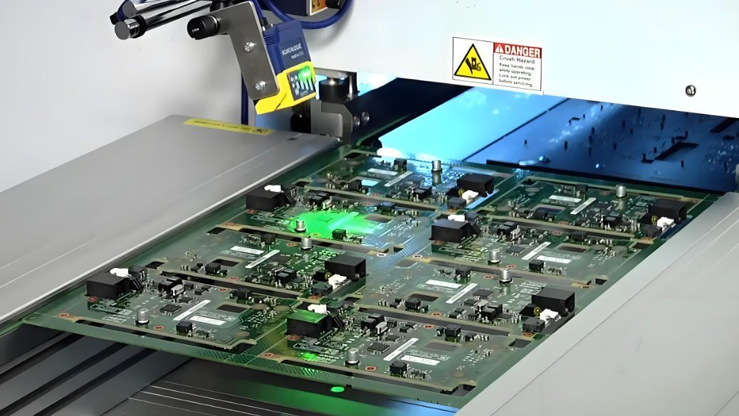
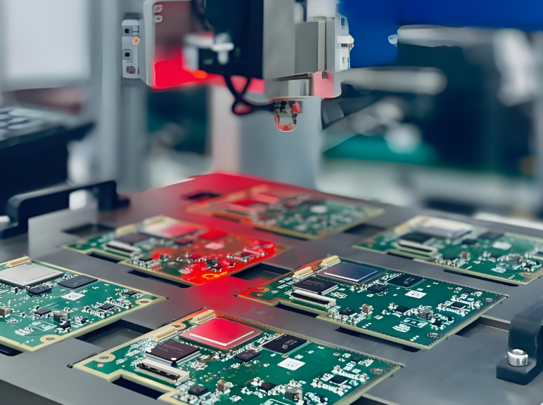
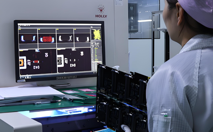
- Process control. Tight lamination curves, AOI after every imaging stage, and X‑ray for BGA registration shrink defect chances.
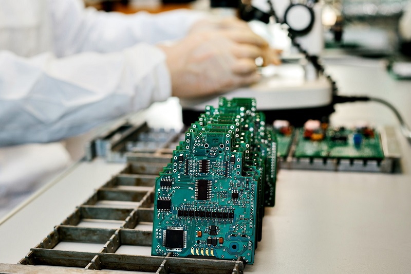
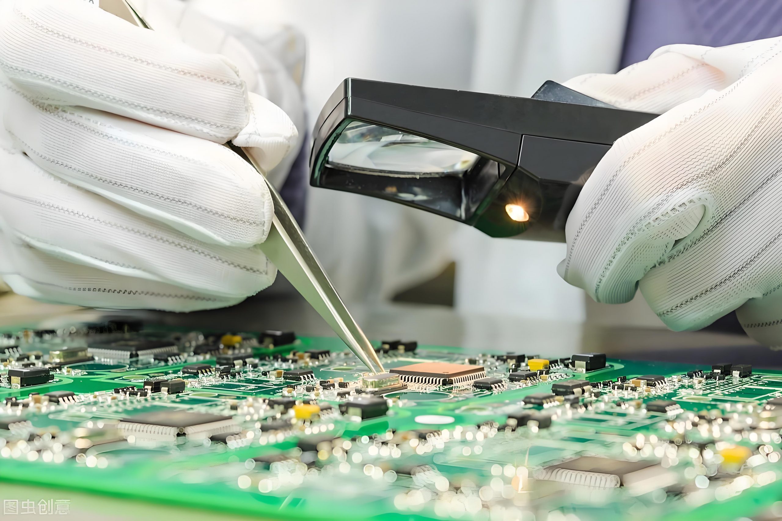
- Final test. Every board passes flying‑probe or bed‑of‑nails electrical test plus 100% visual at microscope stations.
We hold ISO 9001, ISO 13485, IATF 16949, and AS9100D. We have cooperated with customers from all walks of life. High reliability and fast turnaround are the outlets of EBest Circuit (Best Technology).
Why choose EBest Circuit (Best Technology) for your PCB board made in China?
EBest Circuit (Best Technology) has some shiny points as below.
- No more design mishaps. We audit Gerber and CAD files early, fixing shorts or opens before they cost time.
- Stable small‑batch flow. Flexible lines even when order size is low.
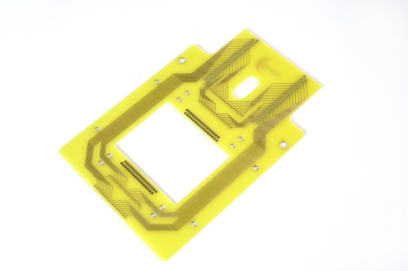
- Material traceability. Approved vendors supply high‑TG FR‑4, high‑frequency PTFE, and ceramic, locking in stable dielectric values.
- Advanced checks. AOI, X‑ray, and SPI catch issues fast, trimming scrap.
- End‑to‑end service. From design support to SMT assembly, one team covers every step. You focus on product, not paperwork.
In short, EBest Circuit (Best Technology) blends modern equipment with a professionalism. The result is dependable PCB boards, on time, every time.
A PCB board made in china offers speed, flexibility, and budget benefits when you pick a proven partner. EBest Circuit (Best Technology) removes worry by pairing strict quality systems with smart automation and quick communication. Our flexible lines switch from prototype to mass build without stress. Reach out to us at sales@bestpcbs.com for specific solutions for your projects.