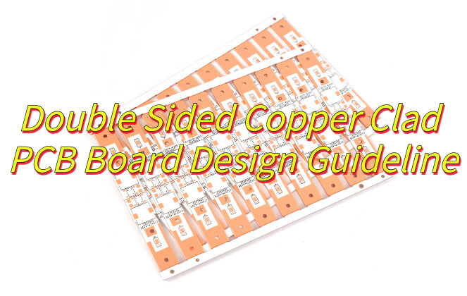
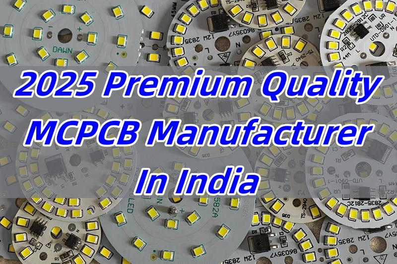
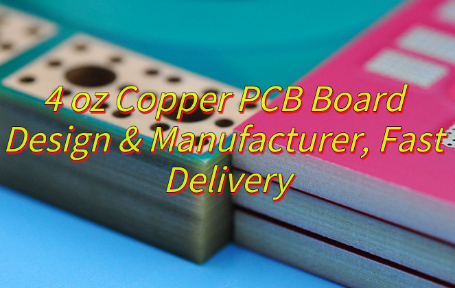
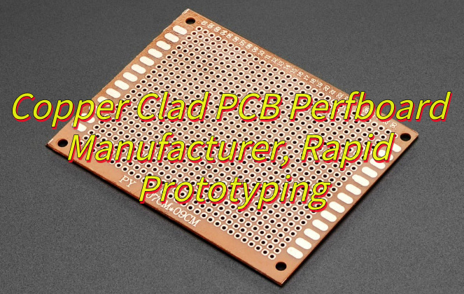
Looking for copper clad PCB perfboard solutions? Let’s discover its components, functions, applications, production process, solder process and clean methods.
Are you troubled with these problems?
- Is traditional PCB performance degradation due to poor heat dissipation?
- Is manual soldering inefficient and resulting in poor product consistency?
- Low-volume production costs and long lead times?
EBest Circuit (Best Technology) can provide service and solution:
- High-thermal-conductivity copper substrate: Utilizing a patented metal substrate, heat dissipation efficiency is increased by 50%, ensuring stable operation of high-frequency circuits.
- Standardized pre-drilled design: Precise 2.54mm hole spacing combined with copper plating simplifies the soldering process and increases product yield by 30%.
- Customized service: 24-hour sample delivery supports flexible small-batch production, reducing customer trial-and-error costs.
Feel free to contact us if you have any request for metal core PCB: sales@bestpcbs.com.
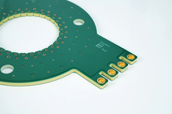
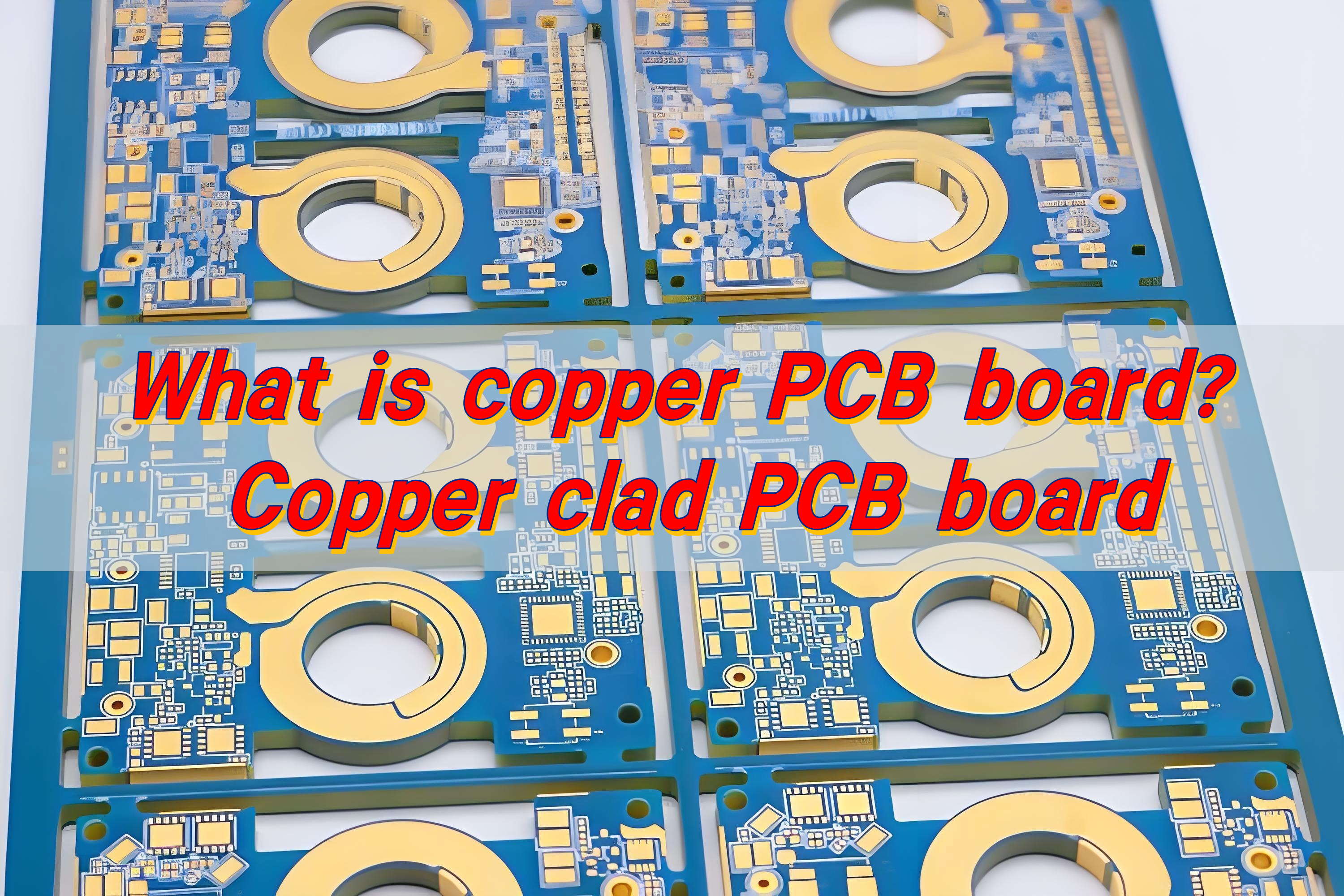
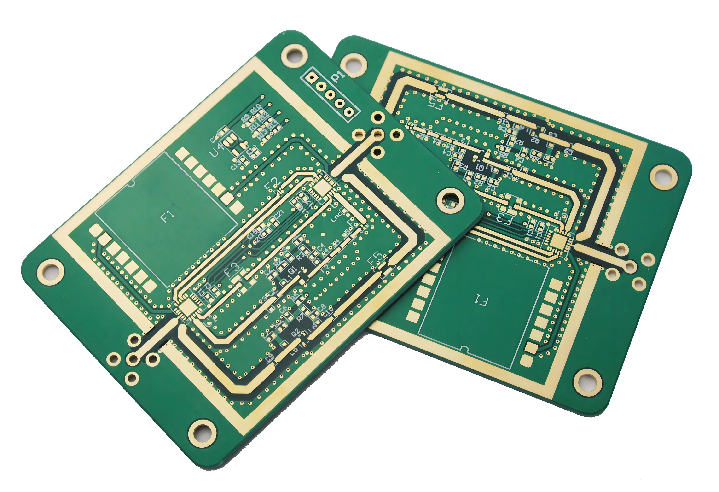
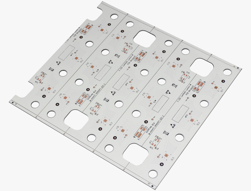
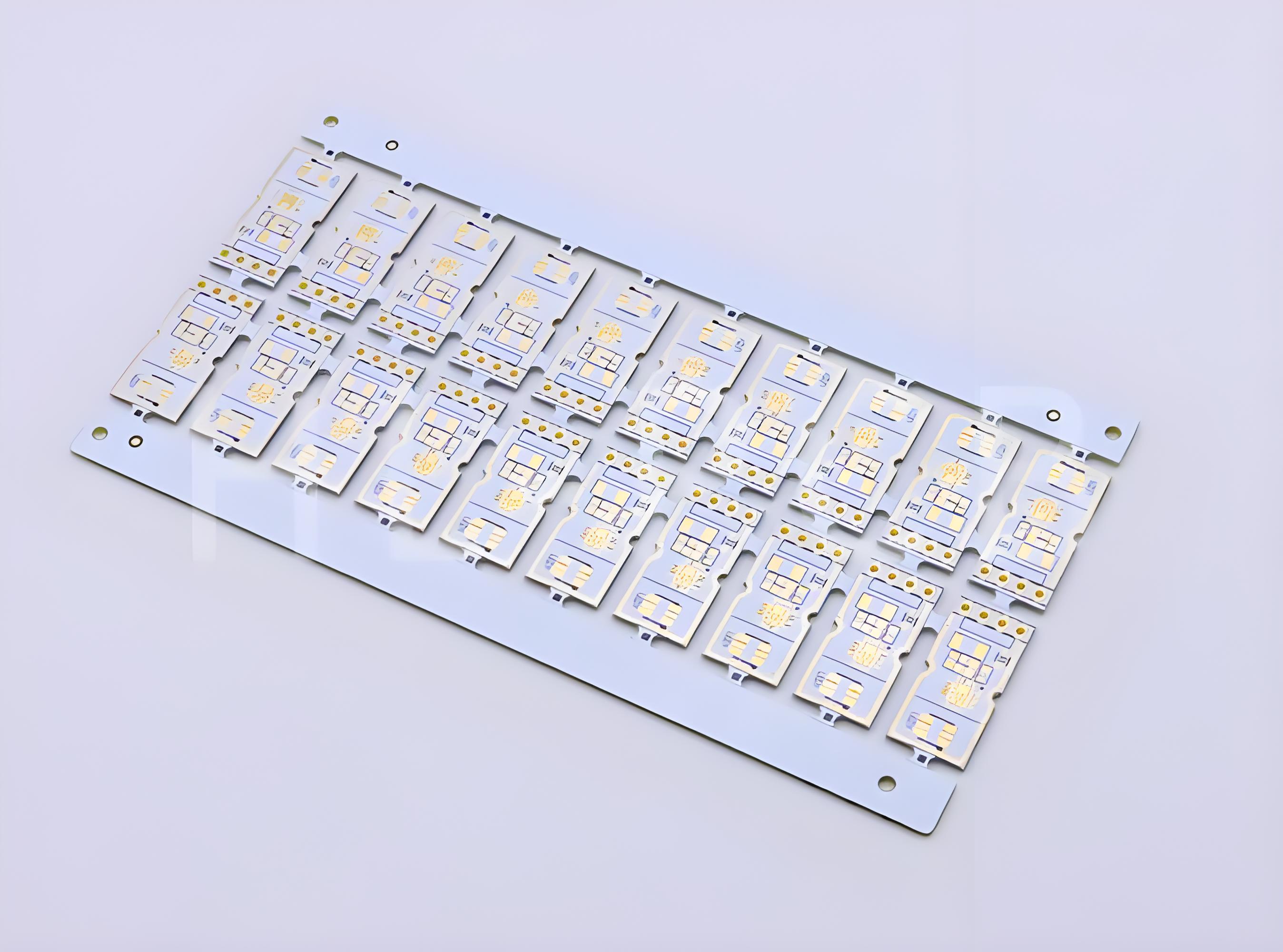
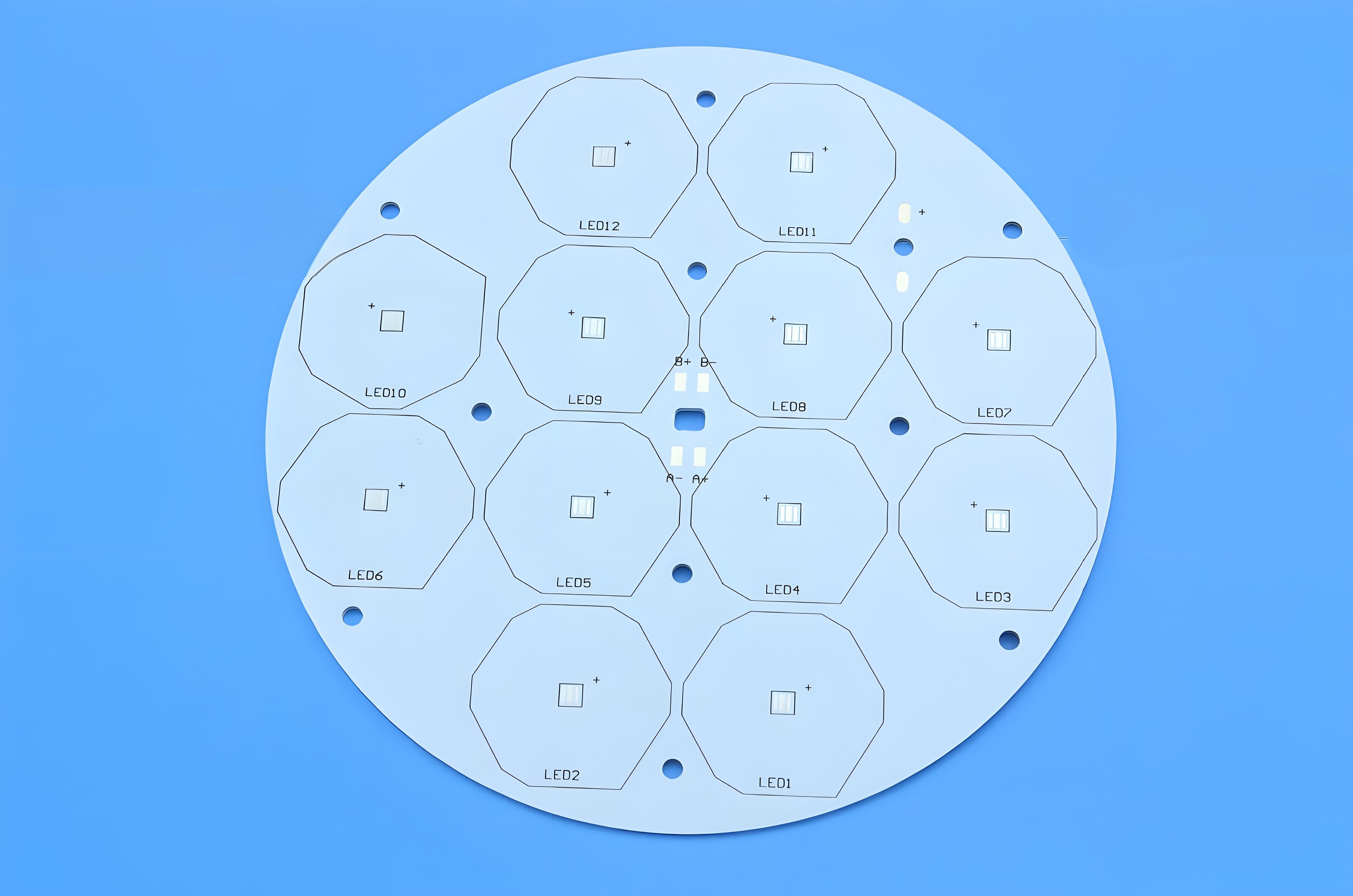
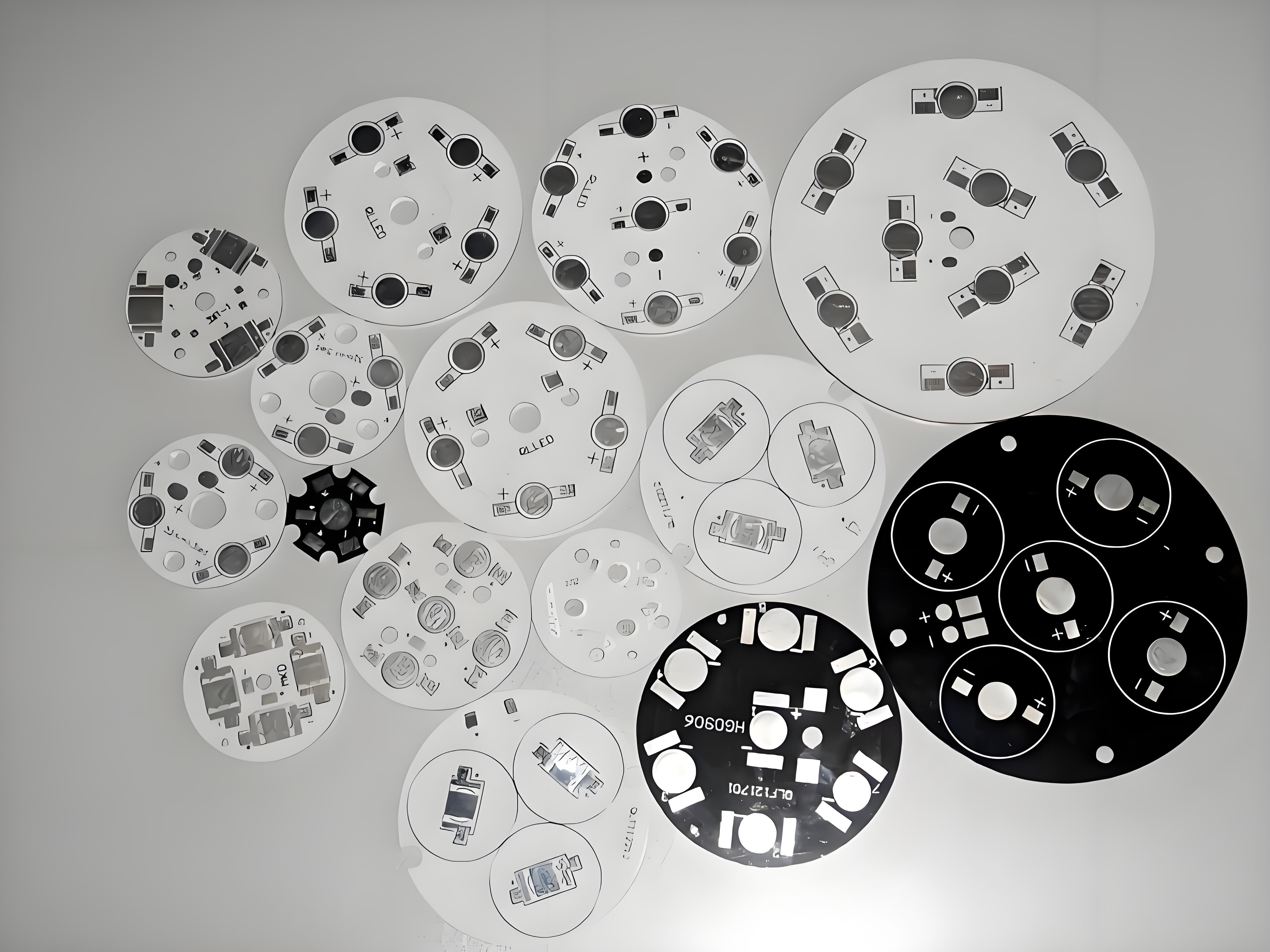
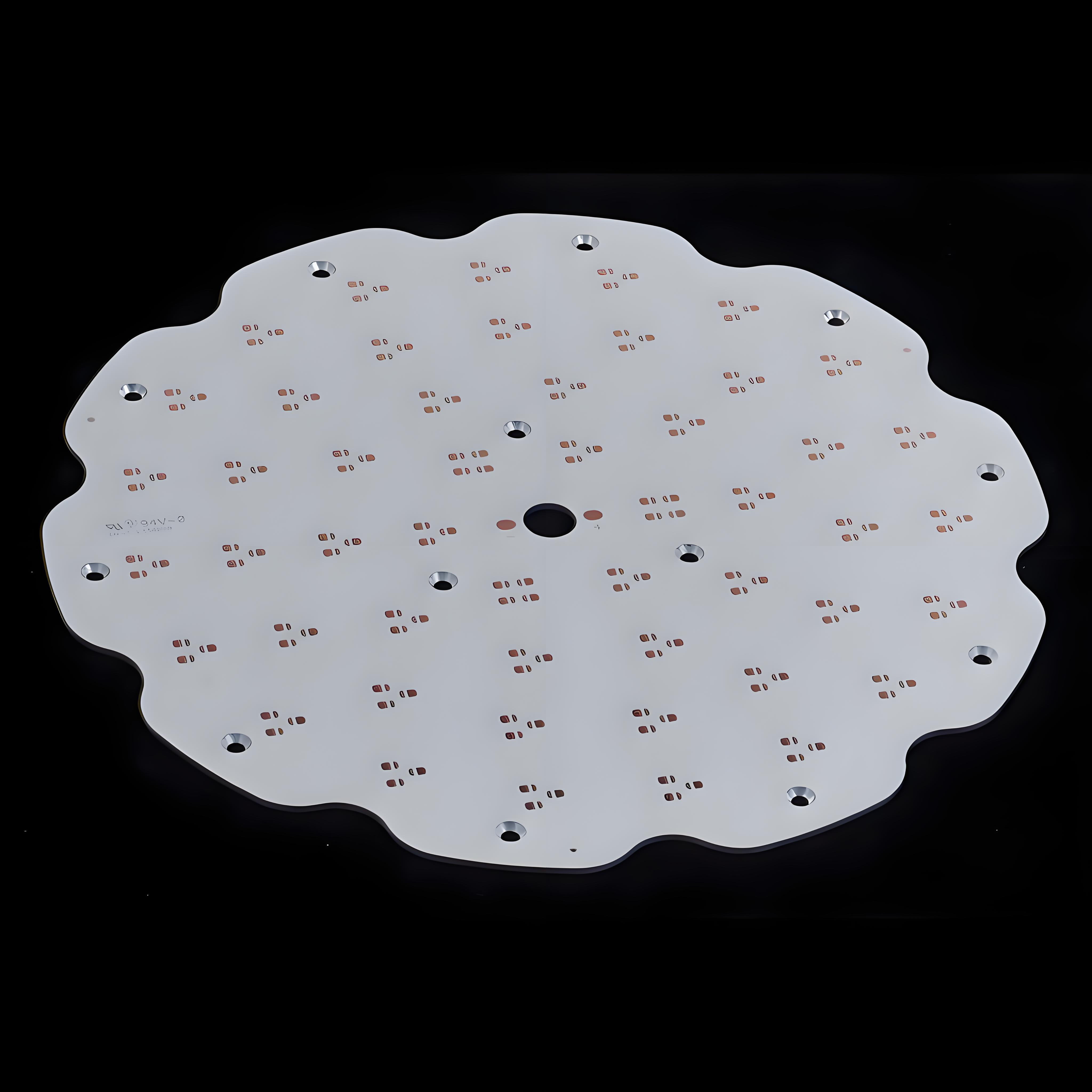
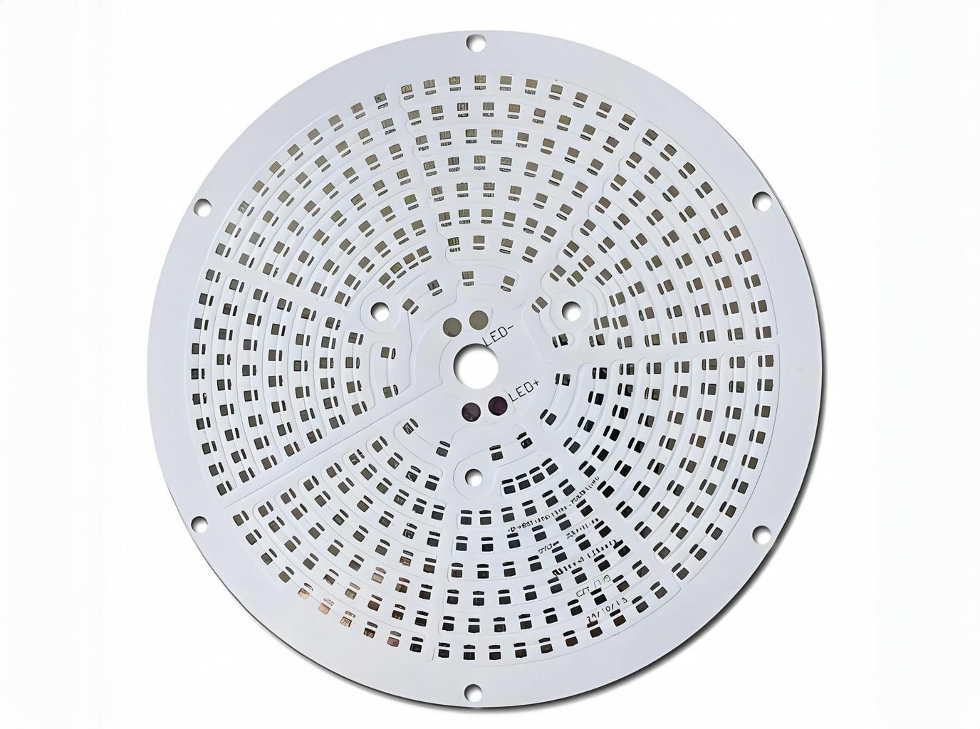
What Is Copper Clad PCB Perfboard?
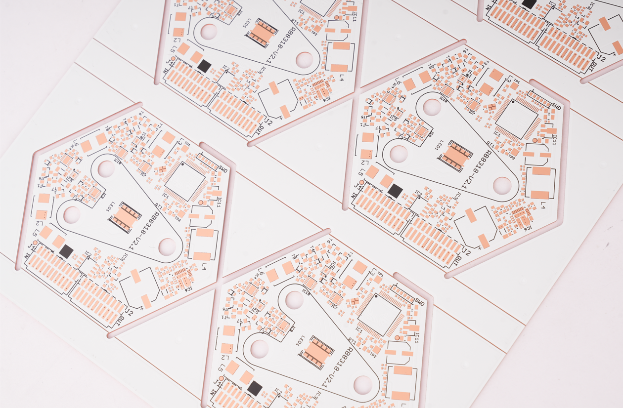
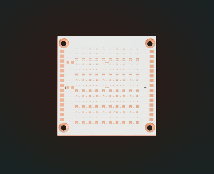
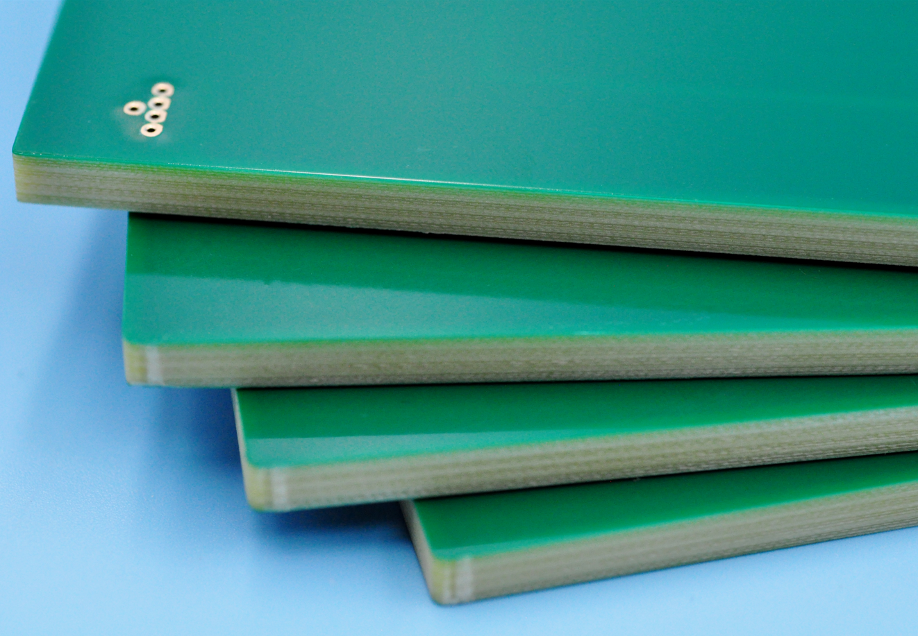
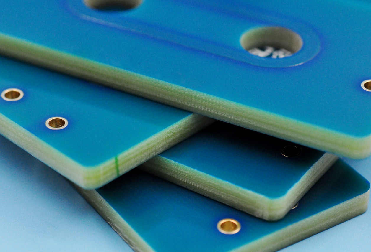
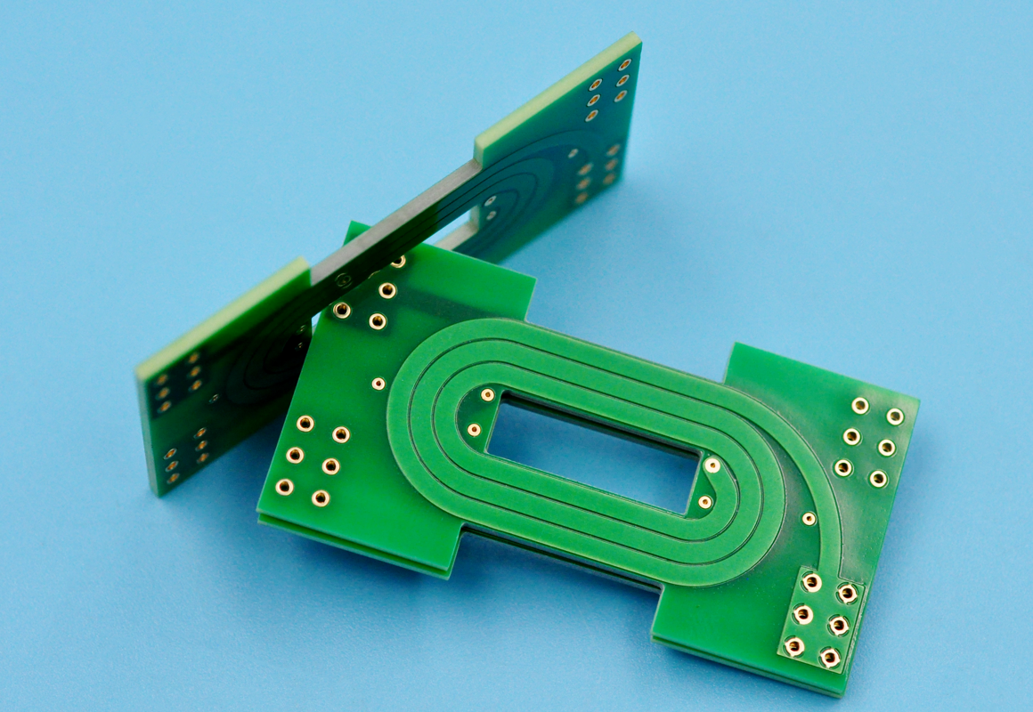
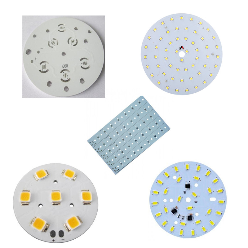
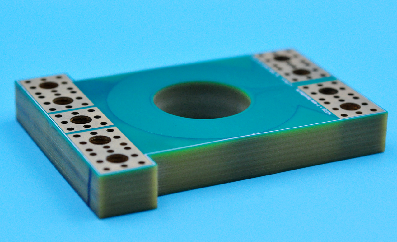
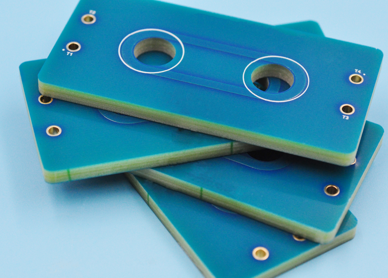
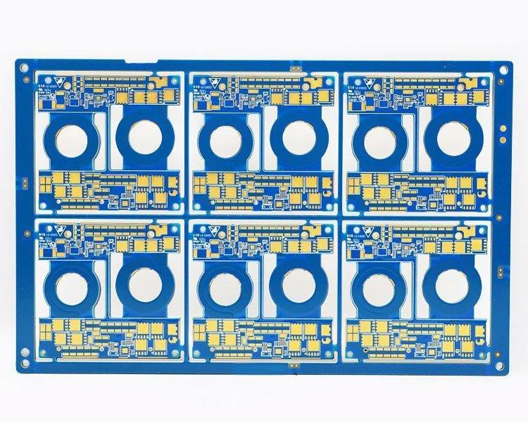
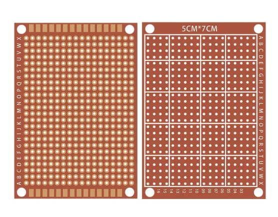
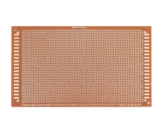
Copper Clad PCB Perfboard (also known as veroboard or stripboard) is a type of printed circuit board (PCB) substrate with a pre-drilled grid of holes (typically spaced 2.54mm apart) and a layer of copper foil bonded to one or both sides of an insulating base material (such as fiberglass or phenolic resin). It is designed for prototyping and experimental circuits, allowing components to be manually soldered to the copper traces and interconnected via jumpers. The copper layer provides conductive pathways for electrical connections while the perforations enable flexible routing without requiring complex PCB fabrication processes. It is widely used in low-to-medium complexity projects due to its simplicity and cost-effectiveness
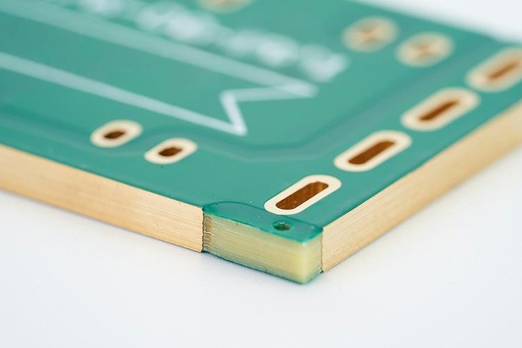
Components of Copper Clad PCB Perfboard
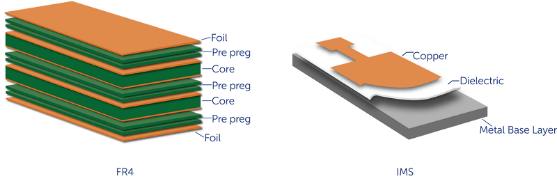
- Base Material: Typically fiberglass (FR-4) or phenolic resin, providing mechanical support and insulation.
- Copper Foil: A thin layer of electrodeposited or rolled copper bonded to one or both sides of the base material for conductive traces.
- Perforated Holes: Pre-drilled holes (usually 2.54mm spacing) for component insertion and interconnections.
- Solder Mask (Optional): A protective coating over copper traces to prevent oxidation and short circuits.
- Silkscreen (Optional): Printed markings (e.g., component labels, polarity symbols) for assembly guidance.
- Tooling Holes: Used for alignment during PCB fabrication or mounting.
Functions of Copper Clad PCB Perfboard
- Prototyping – Enables quick circuit testing without complex PCB manufacturing.
- Educational Use – Ideal for learning soldering and basic circuit design.
- Temporary Wiring – Supports jumper connections for experimental setups.
- Component Mounting – Provides a stable base for mounting electronic components.
- Custom Circuit Assembly – Allows flexible hand-wired connections for unique designs.
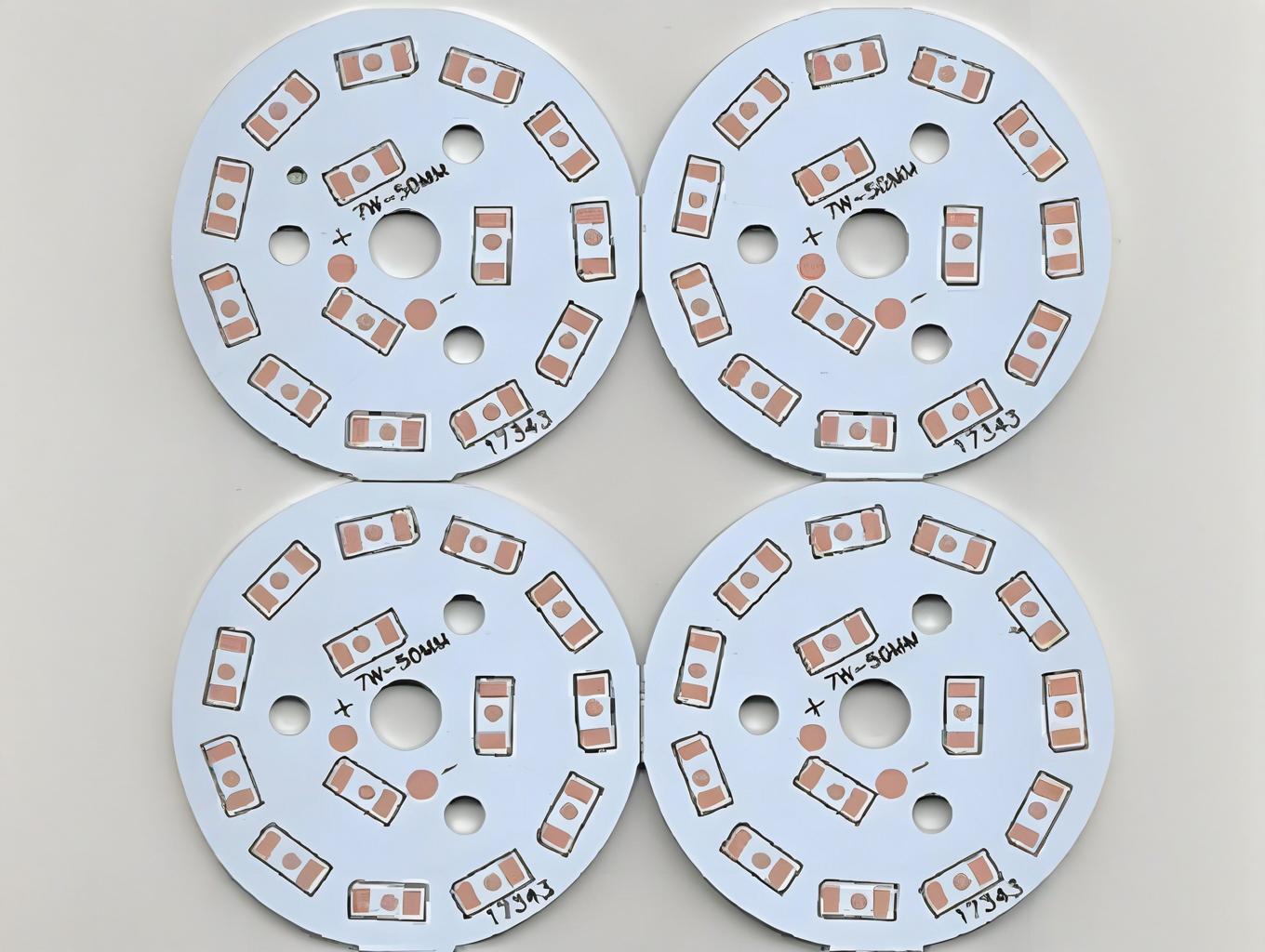
- Heat Dissipation (Aluminum Version) – Some variants improve thermal management.
- Cost-Effective Testing – Eliminates the need for expensive PCB fabrication in early stages.
- Repairability – Circuits can be easily modified or debugged.
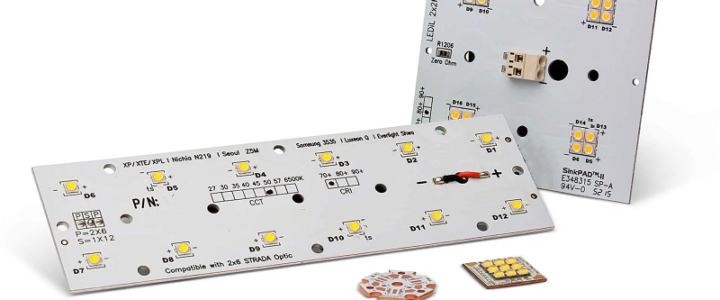
Applications of Copper Clad PCB Perfboard
- Prototyping & Development – Used for rapid circuit testing before mass production, allowing quick iterations.
- Educational Purposes – Ideal for electronics students to learn soldering and circuit design hands-on.
- DIY Electronics Projects – Popular among hobbyists for building custom circuits (e.g., amplifiers, sensors).
- Repair & Modification – Helps fix broken PCB traces or adapt existing circuits with manual rewiring.
- Low-Volume Production – Suitable for small-batch or one-off electronic assemblies where cost matters.
- RF & Analog Circuits – Used in simple RF modules and analog designs due to copper’s conductivity.
- Mechanical Enclosure Wiring – Acts as a backplane for wiring complex machinery or control panels.
- Temporary Circuit Boards – Serves as a non-permanent solution for exhibitions or demo setups.
How to Make A Copper Clad PCB Perfboard?
Copper Clad PCB Perfboard Manufacturing Processes
1. Material Preparation
- Base Material Selection: Typically made from fiberglass-reinforced epoxy resin (FR-4) or phenolic paper, chosen for durability and thermal resistance.
- Copper Foil Lamination: A thin layer of copper (usually 1 oz or 2 oz thickness) is bonded to one or both sides of the base material under heat and pressure.
2. Photolithography (Optional for Custom Designs)
- Photoresist Application: A light-sensitive coating is applied to the copper surface.
- Exposure & Development: UV light exposes the photoresist through a mask, followed by chemical development to create circuit patterns.
3. Etching
- Chemical Etching: Unwanted copper is removed using ferric chloride or ammonium persulfate, leaving the desired traces.
- Rinsing & Drying: The board is thoroughly cleaned and dried to prevent residue.
4. Drilling
- Hole Creation: Precision drilling forms holes for component leads, often using CNC machines for accuracy.
- Deburring: Sharp edges are smoothed to avoid damage during assembly.
5. Surface Treatment
- Plating (Optional): Gold or tin plating may be applied for corrosion resistance and solderability.
- Solder Mask (Optional): A protective layer is added to prevent short circuits.
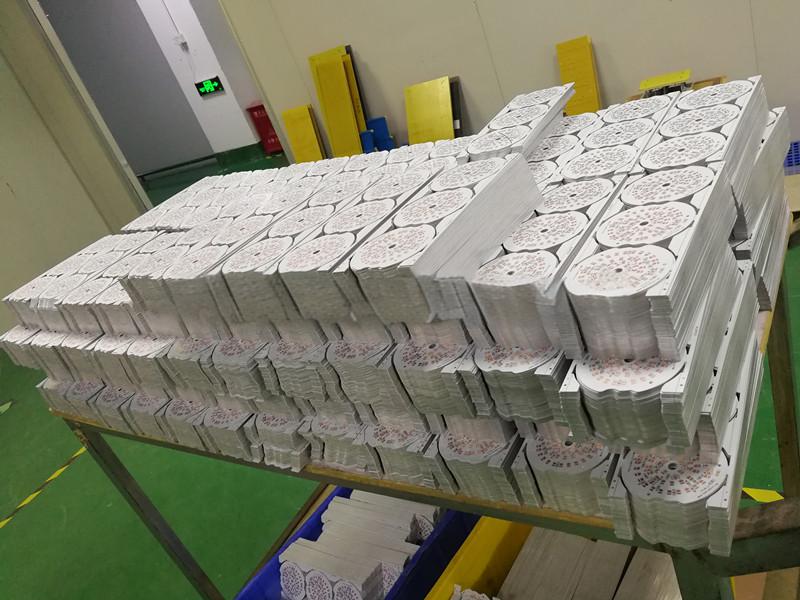
6. Cutting & Finishing
- Sheet Cutting: The large panel is cut into individual perfboards.
- Edge Profiling: Rounded or beveled edges are added for safety.
7. Quality Control
- Electrical Testing: Continuity and insulation tests ensure functionality.
- Visual Inspection: Checks for defects like scratches or incomplete etching.
8. Packaging
- Anti-Static Protection: Boards are wrapped in conductive foam or bags.
- Labeling: Batch numbers and specifications are marked for traceability.
How to Solder Copper Clad PCB Perfboard?
1. Tools Required
- Use a temperature-controlled soldering station (350-400℃) to prevent component damage.
- Select 0.8-1.2mm rosin-core solder wire for optimal flow.
- Prepare fine-tip tweezers, desoldering pump, and flux (optional).
2. Pad Preparation
- Lightly abrade copper pad surfaces with fine sandpaper or steel brush to remove oxidation.
- Apply minimal flux to enhance solder adhesion (thoroughly clean residue in humid environments).
3. Tinning Component Leads
- Dip component leads into solder for 1-2 seconds to form a thin coating.
- Avoid excess solder to prevent short circuits between adjacent pads.
4. Soldering Process
- Secure components: Hold leads with tweezers, position soldering iron at 45° to pad/lead junction.
- Feed solder within ≤3 seconds; achieve conical, shiny joints (rework cold joints immediately).
- Use “drag soldering” for multi-lead components (e.g., ICs) to improve efficiency.
5. Inspection & Correction
- Visually verify solder joints for full coverage, no cold joints, or bridges.
- Test conductivity with multimeter; resolve shorts with desoldering braid.
- Clean flux residues using isopropyl alcohol-soaked swabs.
6. Safety Notes
- Work in ventilated areas; wear safety goggles.
- Use ESD wrist straps for static-sensitive components (e.g., MOSFETs).
- Allow 24 hours post-soldering before power-on testing to avoid latent cold joints.
How to Clean Copper Clad PCB Perfboard?
1. Tools & Materials
- Isopropyl alcohol (≥90%), cotton swabs, soft-bristle brush (e.g., toothbrush).
- Flux remover spray (for heavy residues), ultrasonic cleaner (optional).
- Distilled water, anti-oxidation spray (e.g., clear lacquer).
2. Initial Surface Cleaning
- Dip brush in isopropyl alcohol; gently scrub copper pads to remove flux/rosin.
- Use cotton swabs for tight spaces (e.g., between component legs).
3. Stubborn Residue Removal
- Apply flux remover spray; let sit 10-15 seconds.
- Brush vigorously, then wipe with lint-free cloth.
4. Oxidation Treatment
- Mix 5% citric acid solution (water-based); soak board 2-3 minutes.
- Scrub oxidized areas with brush, then rinse thoroughly with distilled water.
- Avoid strong acids (e.g., muriatic acid) to prevent copper erosion.
5. Drying & Protection
- Blow-dry with compressed air or let air-dry 24 hours (avoid heat guns).
- Apply anti-oxidation spray in thin layers; cure per product instructions.
Copper Clad PCB Perfboard Manufacturer – EBest Circuit (Best Technology)
Reasons why choose EBest Circuit (Best Technology) as copper clad PCB perfboard manufacturer:
- 19-Year Metal Substrate Expertise: Avoid costly design iterations with battle-tested thermal management solutions.
- Strict Quality Control: 100% AOI/X-ray inspection ensures flawless delivery, eliminating rework risks.
- 24-Hour Prototyping: Your Benefit: Cut product validation time by 50% and accelerate market entry.
- ISO 9001/14001 Certified: Global regulatory compliance simplified for seamless international sales.
- Competitive Pricing: Achieve 20%+ cost savings through optimized production scaling.
- Precision Manufacturing (±0.05mm): Enable miniaturized designs for IoT/wearable devices with reliable accuracy.
- Custom Thermal Management: Optimize heat dissipation for high-power applications (e.g., automotive, LED).
- Flexible MOQ (1pcs–100K+): Reduce inventory risks with agile small-batch to mass-production transitions.
- Dedicated Engineering Support: Solve technical challenges proactively, shortening R&D cycles by 30%.
Welcome to contact us if you have request for copper clad PCB: sales@bestpcbs.com.