What is CAM PCB? Let’s discover its function, types, application, design software selection guide, design process and common design issues and solutions.
Are you worried about these issues?
- Perfect design, but constant production issues?
- Low-volume trial production costs too high?
- High-frequency board signal quality consistently substandard?
EBest Circuit (Best Technology) can provide service:
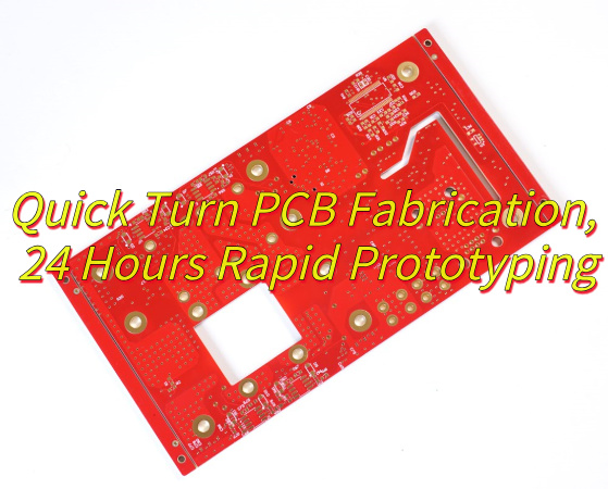
- Free Design for Function (DFM) analysis reduces rework costs by 10%.
- 24-hour rapid prototyping service saves 15% in production costs.
- Material Dk optimization solutions reduce losses by 25%.
Welcome to contact us if you have any request for CAM PCB: sales@bestpcbs.com.
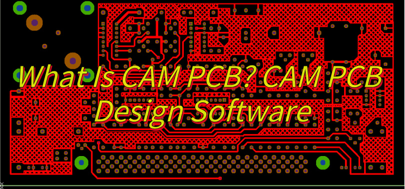
What Is CAM PCB?
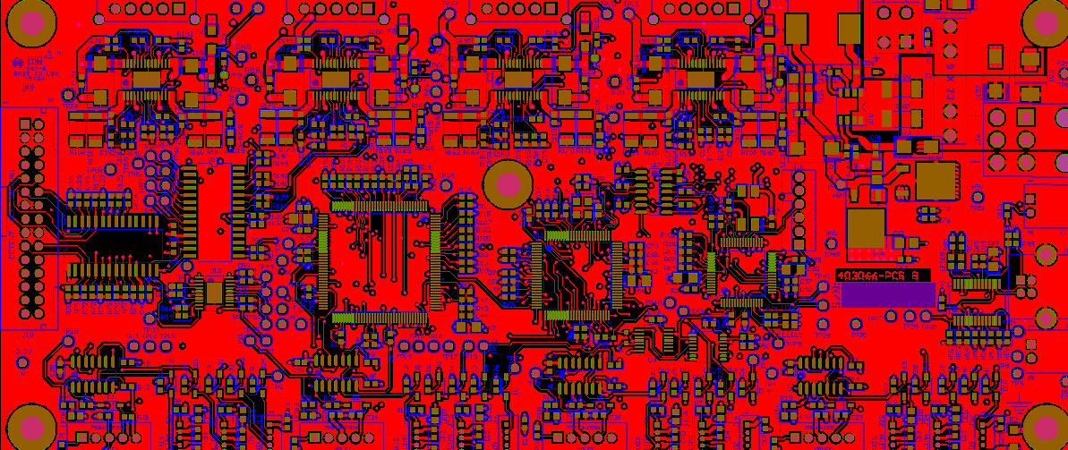
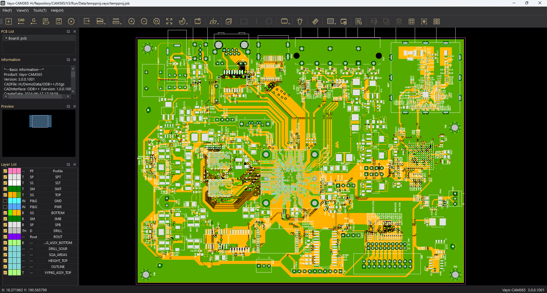
CAM PCB refers to the specialized process of using Computer-Aided Manufacturing software to convert PCB design files (such as Gerber, drill data) into machine-executable production instructions. It optimizes manufacturability by validating designs, compensating for fabrication tolerances (such as etch compensation, impedance control), and generating precision tooling files (photolithography masks, drilling paths) to ensure yield and reliability.
What Are Functions of PCB CAM Design?
Design Rule Validation (DRC)
- Automatically scans for design flaws (e.g., trace width/spacing violations, pad-drill misalignment).
- Prevents defects like solder mask bridging failures and acid traps.
Process Compensation & Optimization
- Adjusts for etching tolerances (±3μm) and material deformation (e.g., ±0.15% scaling for flex PCBs).
- Optimizes laser drilling paths and multilayer via alignment (<25μm offset).
Manufacturing File Generation
- Creates precision files for equipment: photoplotter masks (with anti-glare halftone), optimized drill paths (30%+ idle reduction), and plating current maps (±2μm copper uniformity).
Yield & Cost Control
- Maximizes panel utilization (>93% material efficiency).
- Predicts defects (e.g., copper buildup, undercut).
- Supports advanced processes (rigid-flex transitions, HF ceramic filler avoidance).
What Are Types of CAM PCB Design Software?
Professional CAM Software
- CAM350: Multi-format import (Gerber/Excellon), DFM analysis, netlist comparison, panelization, 3D visualization, NC program generation.
- Genesis 2000: Multi-layer PCB optimization, automated data refinement, workflow integration, direct manufacturing/testing tool output.
- GC-PrevuePlus: Gerber viewing and basic CAM processing.
Integrated CAM Modules in PCB Suites
- Protel-Autotrax: Traxplot for photoplotter files; legacy tool with basic CAM capabilities.
- Altium Designer: Built-in Gerber/drill file generation; primary focus on design with limited CAM features.
Format Conversion & Collaboration Tools
- CAMCAD: Converts PCB formats to neutral standards for cross-department collaboration and design review.
- visECAD: Supports design annotation, intelligent query, and communication between engineers/production teams.
Open-Source & Free CAM Tools
- KiCad: Open-source EDA with Gerber viewer and basic DFM checks; suitable for simple projects/learning.
- PC Gerber: Legacy tool with limited functionality; mostly obsolete.
CNC Programming Specialized Tools
- Copper CAM: Gerber-to-G-code conversion for CNC PCB milling.
- Auto Leveller: Optimizes milling paths when paired with Mach3 control software.
What Are Applications of CAM PCB?
High-Reliability Electronic Devices
- Aerospace Satellite Boards: Laser blind via alignment for 56-layer rigid-flex PCBs.
- Radar Systems: 77GHz millimeter-wave antenna impedance control.
- Medical Implants: Solder mask bridge opening for 0.2mm pitch components in miniature brain-computer interfaces.
Consumer Electronics Mass Production Optimization
- Smartphone HDI Boards: 7-layer laser via stacking and 0.3mm BGA escape routing.
- Wearables: Copper foil stress distribution in dynamic bending zones of flexible battery boards.
High-Frequency High-Speed Systems
- 5G Base Station RF Power Amplifiers: PTFE material Dk value compensation.
- 112Gbps Backplanes: Loss tangent control.
- Data Center GPUs: Synchronous switch noise suppression in 16-layer server motherboards.
Automotive Electronics Safety Control
- Engine ECU Modules: Z-axis CTE compensation for 150°C high-temperature laminates.
- Autonomous Vehicle LiDAR: Phase consistency calibration for microstrip antenna arrays.
Industrial & Energy Applications
- Power Conversion Modules: Thick copper heat dissipation channel design for 10kW SiC inverters
- Oil Exploration Equipment: Drilling parameter optimization for titanium alloy substrates in downhole sensor boards.
How to Choose CAM PCB Design Software?
Core Function Compatibility
- Gerber/ODB++: Prioritize support for latest formats (e.g., Gerber X3) like Valor NPI (Siemens).
- DFM Analysis: Prioritize for real-time rule-checking tools (e.g., CAM350 by DownStream).
- High-Speed Design: Choose Allegro PCB Designer (Cadence) for RF/high-speed PCB optimization.
Industry-Specific Adaptability
- Consumer Electronics: Altium Designer’s CAM module offers cost-effective solutions.
- Automotive/Aerospace: Mentor Xpedition (Siemens) complies with IPC-2581 military standards.
- HDI Boards: Zuken CR-8000 excels in microvia defect detection.
Technical Ecosystem Integration
- EDA Compatibility: Cadence OrCAD syncs with Sigrity signal analysis tools.
- SI/PI Analysis: PADS Professional integrates with HyperLynx for power integrity checks.
Cost Structure Analysis
- Subscription Model: Autodesk Fusion 360 (CAM-enabled) suits SMEs.
- Perpetual License: Pulsonix (UK) offers one-time purchase options.
Localized Service Support
- North America: PCBWeb Designer (free) + BluePrint-PCB (paid CAM plugin).
- EU: EAGLE (Autodesk) automates CE/ROHS compliance validation.
- Asia-Pacific: KiCad (open-source) + GraphiCode GC-Prevue (Japanese toolchain).
Future-Proof Scalability
- AI-Driven DFM: Valor Process Preparation leverages ML for predictive quality control.
- Cloud Collaboration: Altium 365 enables real-time CAM data management across teams.
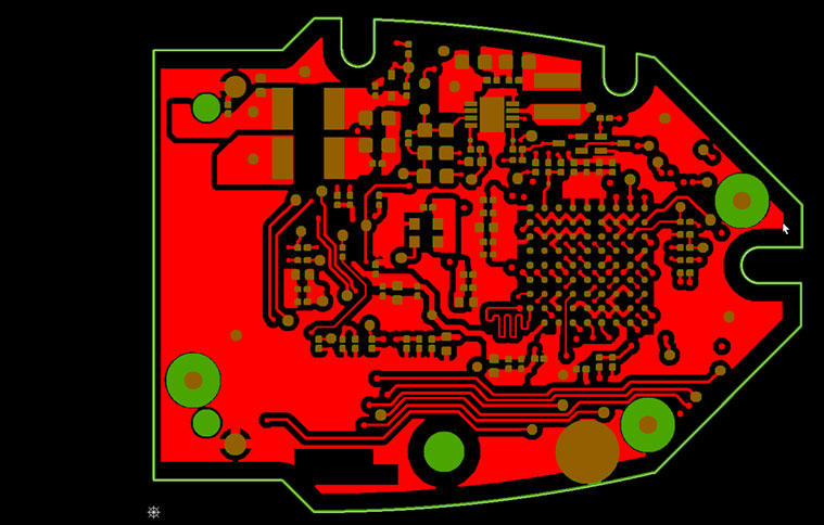
What Is the CAM PCB Design Process?
1. Design File Import
- Load PCB design data (Gerber, ODB++, Excellon, etc.) into CAM software. Verify file integrity and format compatibility for seamless processing.
2. Design Rule Check (DRC)
- Validate critical parameters like trace width, spacing, pad size, and hole dimensions against manufacturing standards. Identify violations to prevent production defects.
3. DFM (Design for Manufacturing) Analysis
- Conduct deep optimization: detect electrical/mechanical issues (e.g., solder mask alignment, minimum hole size), simulate process impacts (e.g., etch compensation, thermal stress), and refine designs for yield enhancement.
4. Panelization & Layout Optimization
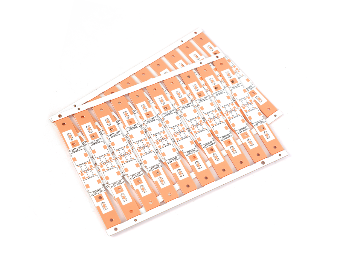
- Arrange multiple PCBs into panels for efficient production. Apply algorithms for material utilization, nesting precision, and toolpath optimization to minimize waste and machining time.
5. Manufacturing File Generation
- Output production-ready files: photoplotter data (Gerber), drilling programs (NC/Excellon), milling paths, assembly drawings, and process-specific documentation (e.g., solder paste stencils).
6. Cross-Verification & Simulation
- Validate outputs through 3D visualization, signal integrity checks, and thermal simulations. Ensure files meet device-specific requirements (e.g., light painting machine resolution, pick-and-place compatibility).
7. Final Validation & Archiving
- Perform end-to-end verification of manufacturing files. Store processed data with version control and audit trails for traceability. Archive for future revisions or quality audits.
FAQs of CAM PCB Design
Q1: How to handle design file import anomalies in CAM PCB?
A1: Use CAM software supporting multi-format import (e.g., CAM350) to validate file integrity and compatibility. Standardize data sources with conversion tools (e.g., CAMCAD) to prevent manual errors.
Q2: What are solutions for DRC violations in CAM processing?
A2: Implement strict IPC-standard rule libraries in CAM tools (e.g., CAM350) to auto-flag violations. Leverage 3D visualization for precise fault localization and prioritize critical adjustments like impedance matching for high-speed lines.
Q3: How to address DFM defects like solder mask misalignment?
A3: Enable DFM modules for deep simulation (e.g., etch compensation, thermal stress analysis). Optimize material parameters (e.g., PTFE Dk compensation) and adopt iterative validation for process refinement.
Q4: How to improve panelization efficiency?
A4: Apply intelligent nesting algorithms (e.g., Genesis 2000) with optimized spacing rules (e.g., ≥1mm margins) and toolpath planning to achieve >85% material utilization.
Q5: What causes signal/thermal failures and how to mitigate?
A5: Use SI/PI tools (e.g., HyperLynx) for signal integrity validation and thermal simulators (e.g., ANSYS) for heat distribution prediction. Implement thermal via arrays (≥10% copper coverage) in high-power zones.