A flex connector PCB is a specialized interconnect that merges a flexible printed circuit board with integrated or attached connectors, serving as the critical nervous system for modern compact and flexible electronics. This article will comprehensively explore their types, design considerations, and application-specific best practices, providing a roadmap for implementing robust interconnects in space-constrained and dynamic devices.
Engineers aiming for smaller, lighter, and more flexible devices often struggle with the critical question of how to ensure reliable interconnects in tight and dynamic environments.
- Signal Degradation and EMI: High-speed signals easily suffer loss and interference in dense, flexible layouts.
- Space and Weight Constraints: Traditional connectors take too much space and add unwanted weight.
- Mechanical Fatigue: Repeated bending causes cracks, delamination, and connector detachment.
- Assembly Errors: Misalignment or mishandling of fragile flex connectors leads to damage and defects.
- Environmental Vulnerability: Moisture, dust, and chemicals corrode contacts and reduce reliability.
These challenges can be solved with optimized flex design and application-specific connector strategies tailored for compact electronics.
- Impedance-Controlled Flex Design: Controlled impedance and shielding maintain clean signal performance.
- HDI and Miniaturized Connectors: Compact HDI layouts and small-pitch connectors maximize density.
- Reinforced Bend Areas: Proper bend radii, stiffeners, and flex-rated connectors prevent fatigue failures.
- DFM and Foolproof Interfaces: Guided features and robust ZIF locks reduce assembly errors.
- Environmental Protection: Waterproof connectors and protective coatings ensure long-term durability.
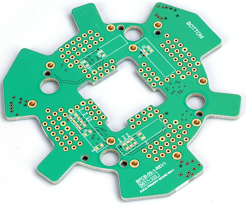
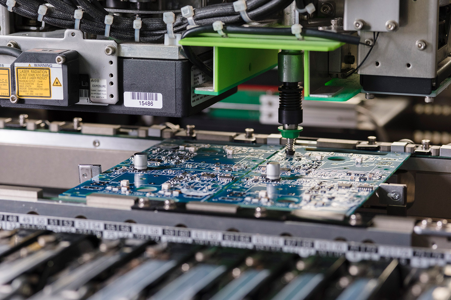
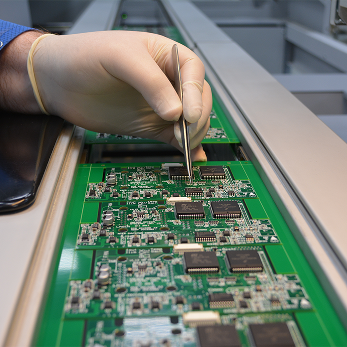
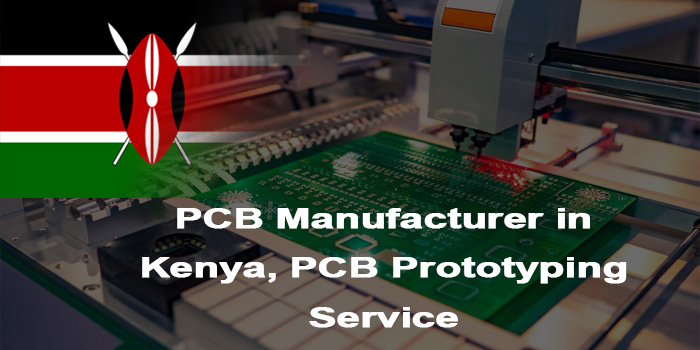
As an experienced PCB manufacturer and assembly partner, EBest Circuit (Best Technology) provides end-to-end support—from selecting the right flex PCB connector types to designing the flex connector PCB layout and delivering precise, reliable manufacturing. With ISO 13485 medical and AS9100 aerospace certifications, and fully traceable MES-driven PCB and SMT lines, we ensure the quality required for critical applications. We also support small-batch builds with no MOQ, helping you innovate faster without production limits. For project support, contact us at sales@bestpcbs.com.
.
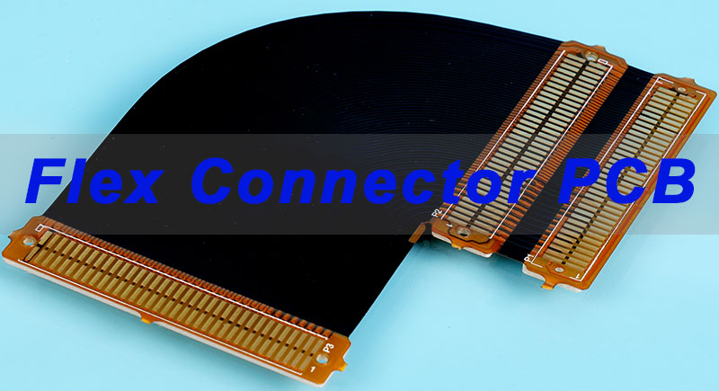
What Is a Flex Connector PCB and Why It Matters in Compact Electronics Design?
A Flex Connector PCB refers to the integration point where a flexible printed circuit (FPC) terminates, often incorporating or interfacing with a specialized connector. This is not just a simple junction; it’s a critical engineered interface designed to maintain electrical continuity and mechanical integrity while accommodating movement, space constraints, and harsh environments. In compact electronics, this component is indispensable as it bridges the gap between rigid subsystems and dynamic flexing elements, enabling the three-dimensional packaging essential for modern wearables, foldable phones, and miniaturized medical tools.
The core value of this technology lies in its ability to solve fundamental design conflicts:
- Space Efficiency: It eliminates the need for bulky wiring harnesses and large connector headers.
- Weight Reduction: Replaces heavier alternative interconnects, crucial for portable devices.
- Reliability in Motion: Designed to withstand repeated bending, vibration, and torsion where rigid boards would fail.
- Assembly Simplification: Can reduce the number of individual interconnection parts and process steps.
To understand its impact, consider the comparison below:
| Interconnect Method | Typical Use Case | Relative Space | Reliability in Flexing |
|---|---|---|---|
| Wire Harness & Discrete Connector | Traditional enclosures | High | Low (Stress on solder joints) |
| Standard FPC with Soldered Connector | Limited-space static link | Medium | Medium (Stress at connector junction) |
| Engineered Flex Connector PCB Assembly | Wearables, hinges, dynamic zones | Very Low | High (Designed for stress) |
In summary, a flex connector PCB is the enabling technology that allows electronics to conform to new forms and functions, making it a cornerstone of innovation in compact device design.
Key Flex PCB Connector Types and How They Influence Signal Integrity and Reliability
Choosing the correct flex PCB connector type is paramount, as the connector acts as the gatekeeper for signal and power integrity. The selection directly influences electrical performance, mechanical robustness, and assembly yield. The primary categories include:
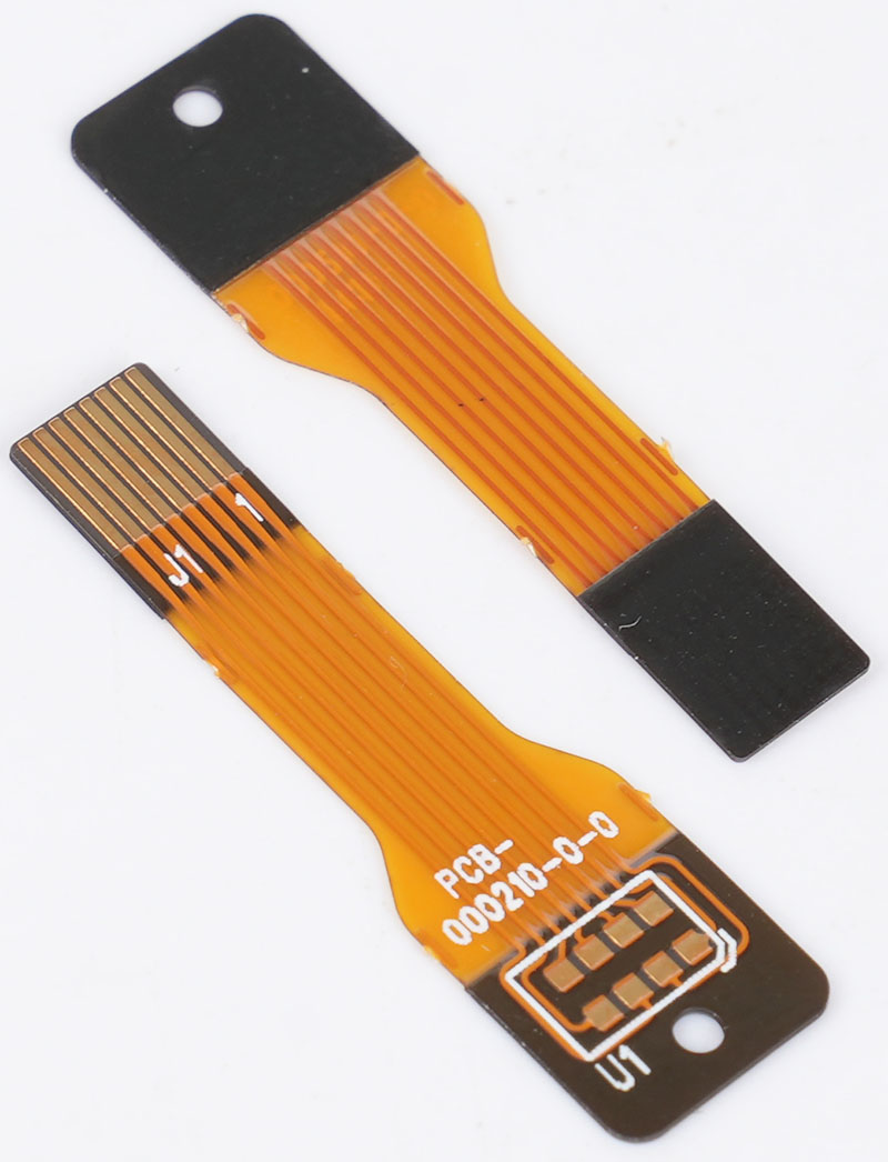
- ZIF (Zero Insertion Force) & LIF (Low Insertion Force) Connectors: These use a sliding or flipping clamp mechanism to secure the flex PCB edge connector portion. They are excellent for delicate, high-density flex tails as they prevent insertion damage. ZIF slide locking connector for flex PCB designs are ubiquitous in consumer electronics for internal display and camera links.
- FFC/FPC Connectors (Flat Flexible Cable/PCB Connectors): Often used interchangeably, these are the most common type for connecting a separate flat cable or the tail of an FPC. They provide a simple, low-profile connector flex PCB interface.
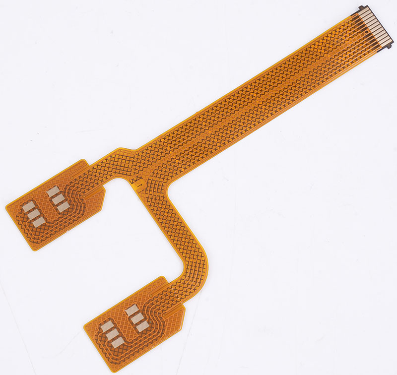
- Board-to-Board Connectors: Used in rigid flex PCB connector applications, these connect a flex circuit directly to a rigid PCB. They come in stacking, mezzanine, or coplanar arrangements, enabling complex 3D architectures.
- Soldered Direct Attachment: The flex PCB to wire connector or rigid board connection is made via direct soldering (reflow, hand-solder). This is the most space-efficient and cost-effective method but offers no serviceability and requires careful strain relief.
- Specialized Connectors: This includes waterproof flex PCB connector for harsh environments, high-speed mezzanine connectors for data buses, and custom flex PCB cable connector solutions for specific mechanical requirements.
The connector’s construction—its contact material, plating (often gold for reliability), pitch, and housing—directly affects signal integrity. A poor-quality knockoff PCB flex connector may have inconsistent plating, leading to increased contact resistance and intermittent failures. Furthermore, improper impedance matching at the connector transition can cause signal reflections, especially critical in high-speed applications like those using RGB LED PCB flex connectors with fast data protocols. In essence, the connector type defines the reliability ceiling of the entire interconnect system.
How Flex PCB Connectors Enable High-Density Interconnects in Wearables and Portable Devices?
The drive for thinner, lighter, and more feature-rich wearables and portable devices demands extreme component density. Flex PCB connectors are pivotal in achieving this by enabling three-dimensional wiring in spaces where traditional boards cannot go. They act as the dynamic, high-density bridges between multiple rigid sub-assemblies.
Key enabling strategies include:
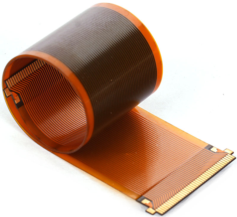
- 3D Packaging Freedom: Flex circuits can fold, twist, and bend around batteries, sensors, and housings. The connectors for flex PCB at their termini allow these circuits to be modularly connected to main boards and displays, stacking functionality in the Z-axis.
- Fine-Pitch Compatibility: Modern flat flex PCB connector systems support pitches down to 0.2mm, allowing a large number of signals to pass through a very narrow flex cable PCB connector profile. This is essential for connecting high-resolution displays or multi-sensor arrays.
- Reduction of Point-to-Point Wiring: A single flex with integrated connectors can replace dozens of discrete wires, simplifying assembly, reducing weight, and improving reliability by minimizing solder joints.
- Integration with Rigid-Flex Designs: In a rigid flex PCB or connector strategy, the connector is often eliminated altogether at critical interfaces; the flex material seamlessly transitions into the rigid board, creating the most reliable and dense interconnect possible.
Consider a smartwatch: a flex circuit PCB connector links the main processor board to the display, another connects to the heart-rate sensor on the back, and a third may interface with the charging port. Each of these connections must be ultra-compact, reliable over millions of flex cycles, and easy to assemble. Flex PCB connectors make this intricate electronic “skeleton” possible, directly enabling the sleek, unified designs consumers demand.
Design Guidelines for Selecting the Right Flex PCB Edge Connector in Space-Constrained Layouts
Selecting a flex PCB edge connector—the point where the flex tail interfaces with its receptacle—requires balancing electrical, mechanical, and spatial demands. In compact layouts, the right choice directly affects performance and reliability.
Follow this selection and design framework:
| Guideline Category | Key Considerations (Condensed) |
|---|---|
| Electrical Requirements | Current rating / Pitch & signal count / Impedance matching |
| Mechanical & Spatial Fit | Footprint & height / Mating direction / Locking type |
| Reliability & Durability | Mating cycles / Retention force / Stress relief |
| Assembly & Serviceability | Tool access / Alignment features / Reworkability |
Electrical Requirements:
Choose a connector that supports required current, fits your signal density (e.g., 0.3–0.5 mm pitch), and maintains impedance continuity for high-speed lines.
Mechanical & Spatial Fit:
Review 3D height and footprint early in your CAD model. Select top-, bottom-, or side-entry options based on assembly access, and prioritize reliable locking styles such as ZIF/LIF.
Reliability & Durability:
Evaluate connector mating cycles, vibration resistance, and proper stress-relief design—especially around the flex heel where failures frequently occur.
Assembly & Serviceability:
Ensure tools can actuate the latch safely, include alignment cues to prevent reverse insertion, and consider connectors that can be replaced if rework is expected.
In summary, the optimal flex connector to PCB is not simply the smallest available; it is the one that fits your electrical needs, survives your mechanical environment, and supports error-free assembly over the product’s lifetime.
Rigid Flex PCB Connector Considerations for Hybrid Structures and Dynamic Bending Zones
Rigid flex PCB connector strategies are central to hybrid rigid-flex designs, where the goal is often to minimize or optimize connector usage. The decision often comes down to a choice: use discrete connectors at the rigid-flex junction, or design the flex to extend directly into the rigid area as an integral “connector” (a plated finger region).
Critical considerations for dynamic areas include:
- Bend Radius Compliance: The most fundamental rule. Ensure the flex PCB connector and adjacent traces are placed outside the minimum bend area. The minimum bend radius is typically 6-10x the flex thickness for dynamic flexes. Violating this causes immediate or fatigue-induced failure.
- Neutral Axis Design: For multi-layer flexes in bending zones, try to balance copper layers symmetrically around the center (neutral axis) to prevent stress concentrations that can lead to delamination.
- Stiffener Application: Use polyimide or FR4 stiffeners underneath connectors flex PCB areas to provide a stable, flat mating surface and prevent flexing at the solder joints. This is non-negotiable for any attached component.
- Transition Zone Reinforcement: The area where the flex transitions to rigid (or where a connector is placed) is a high-stress point. Use curved corners in the copper and coverlay, and avoid placing vias in this region.
- Strain Relief Features: Design mechanical features into the enclosure or use adhesive anchor points to ensure that any flexing motion is distributed along the intended bend area, not at the connector interface.
For instance, in a device with a folding screen, the rigid flex PCB connector between the main body and display must be carefully placed within a rigid section, with the dynamic bend occurring in a dedicated, reinforced flex zone away from any components. The integrity of the entire product depends on this zoning discipline.
How to Open a Flex Cable PCB Connector Safely During Assembly and Rework Processes?
Knowing how to open a flex cable PCB connector is a critical manual skill in assembly and repair. Improper technique is a leading cause of damage to both the connector and the fragile flex tail. The process varies slightly by connector style but follows a universal principle: release the locking mechanism before pulling the cable.
A general safe procedure is as follows:
- Identify the Lock: Visually inspect the connector. Most ZIF slide locking connector for flex PCB types have a small, liftable flap or a sliding latch. A flat flex PCB connector may have a clamp-type lever.
- Use the Correct Tool: Never use a metal screwdriver or sharp tool that can slip and damage the PCB. Use a dedicated nylon or plastic spudger.
- Actuate the Lock:
- For a flip-type ZIF lock: Gently insert the spudger tip under the edge of the raised locking flap and lift it to a 90-degree (or as specified) open position.
- For a slide-type ZIF lock: Use the spudger to carefully push or slide the tiny latch in the direction indicated (often marked with an arrow).
- Remove the Flex: Once the lock is fully disengaged, the flex cable will be loose. Grip it evenly by its stiffened ends (not by the conductors) and pull it straight out, avoiding any twisting or bending.
- For Re-insertion: Ensure the flex is correctly oriented (observe polarity marks), insert it fully into the slot, and then carefully close or slide the lock back until it clicks or is fully seated. You should feel positive engagement.
Applying excessive force during any step is the primary cause of breaking the latch, tearing the flex, or lifting pads. Training and proper tools are essential to prevent yield loss, especially when dealing with proprietary connectors like a specific flex PCB connector 487526 or flex PCB connector 487526-9.
Environmental and Mechanical Requirements for Waterproof Flex PCB Connector Applications
Devices used in outdoor, medical, and industrial environments require waterproof flex PCB connector solutions designed to keep out moisture, dust, and contaminants. Achieving this level of reliability demands careful attention to key environmental and mechanical parameters.
Key requirements and considerations include:
| Requirement | Key Focus (Condensed) |
|---|---|
| Ingress Protection (IP Rating) | Required IP level (IP67/IP68) |
| Sealing Methodology | Gaskets / O-rings / Potting / Membrane |
| Material Compatibility | Chemical, UV, and temperature resistance |
| Mechanical Robustness | Vibration, shock, and locking strength |
| Pressure Equalization | Venting features to balance pressure |
Ingress Protection (IP Rating):
Choose the appropriate IP67 or IP68 rating depending on the exposure to water and dust during device operation.
Sealing Methodology:
Use the right sealing approach—such as gaskets, O-rings, potting compounds, or membrane seals—based on environmental severity.
Material Compatibility:
Select housing and sealing materials that resist chemicals, UV exposure, and temperature swings. Silicone is commonly used for reliable sealing.
Mechanical Robustness:
Ensure the connector maintains its seal under vibration and shock; prioritize strong locking mechanisms and strain-relief features.
Pressure Equalization:
In applications facing pressure changes, use venting elements that pass air while blocking liquid ingress.
In a nutshell, in products such as waterproof wearables or automotive sensors, a waterproof flex PCB connector is not optional—it is essential for long-term reliability. The flex circuit PCB connector region may require conformal coating or encapsulation to achieve a fully sealed system.
Common Failure Modes of Connectors for Flex PCB and How to Prevent Knockoff PCB Flex Connectors Issues
Even a well-designed interconnect can fail if the components are subpar. Understanding common failure modes of connectors for flex PCB is key to prevention, and a major risk factor is the use of counterfeit or knockoff PCB flex connectors.
Common Failure Modes:
- Contact Wear/Corrosion: Poor plating on contacts leads to increased resistance, intermittent connections, and eventual open circuits.
- Plastic Housing Degradation: Inferior plastic can become brittle with temperature cycling or UV exposure, causing housing cracks or latch breakage.
- Poor Contact Retention Force: Contacts lose spring tension, leading to a loose connection that fails under vibration.
- Misalignment & Improper Mating: Damaged guide posts or out-of-spec tolerances cause misinsertion, bending contacts or damaging the flex tail.
- Stress Fractures at Solder Joints: This occurs when the flex is repeatedly bent too close to the connector due to lack of strain relief.
How to Prevent Issues from Knockoff Components:
- Source from Authorized Distributors: This is the single most effective step. Avoid gray market sources with prices that seem “too good to be true.”
- Implement Incoming Inspection: Use microscopes to check plating quality, gauges to verify pin alignment and housing dimensions, and test samples for retention force.
- Audit Your Supply Chain: Know your supplier’s source. Reputable manufacturers like EBest Circuit (Best Technology) have transparent and vetted supply chains for all components, including PCB flex connectors.
- Demand Full Documentation: Legitimate parts come with datasheets, material certificates, and traceability lot codes. Counterfeits often have copied or missing documentation.
- Test Under Application Conditions: Subject samples to thermal cycling, humidity, and mechanical stress tests that mimic your product’s lifecycle before committing to a production run.
Investing in genuine, high-quality flex PCB connectors from reliable partners mitigates these failure risks at the source, ensuring the long-term reliability promised by your innovative compact device design.
All in all, flex connector PCB technology is the essential enabler that allows electronics to break free from rigid, boxy confines and integrate seamlessly into our flexible, portable, and wearable world. This article has explored the critical aspects—from core definitions and flex PCB connector types to advanced design guidelines and failure prevention—that ensure these delicate yet robust interconnects perform reliably.
Mastering flex connector PCB design is not merely a technical task; it is a strategic advantage in creating competitive, next-generation devices. It requires a partner with deep material knowledge, precision manufacturing capabilities, and a commitment to quality. EBest Circuit (Best Technology) possesses precisely this expertise, offering comprehensive solutions from design support through to the production of reliable rigid-flex assemblies and the supply of genuine, high-performance connectors flex PCB. A warm welcome to contact our engineering team anytime at sales@bestpcbs.com to discuss your connector flex PCB project requirements.