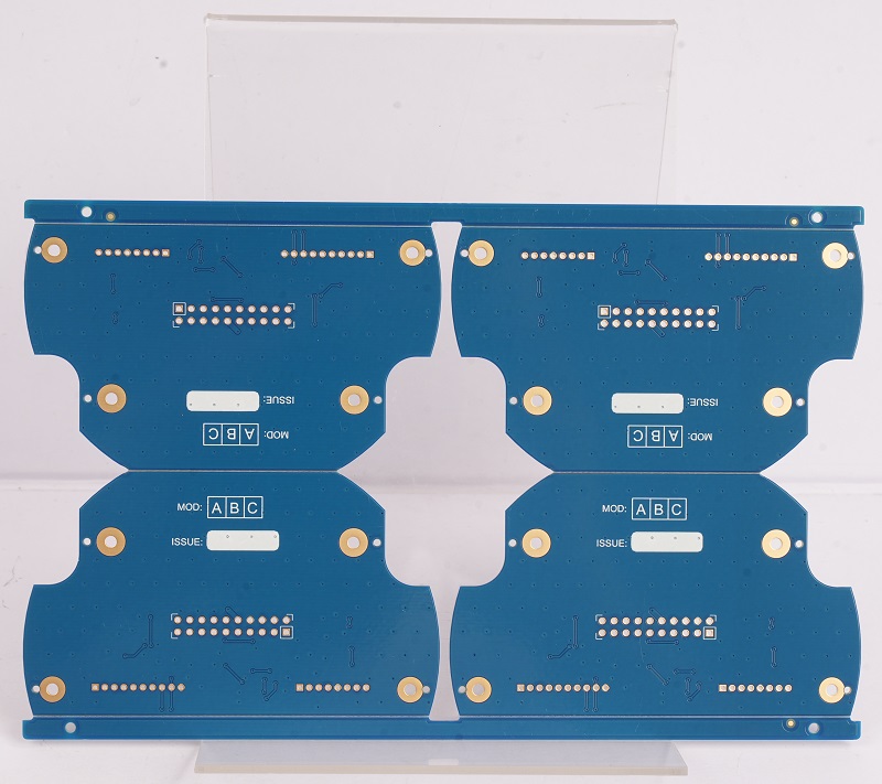
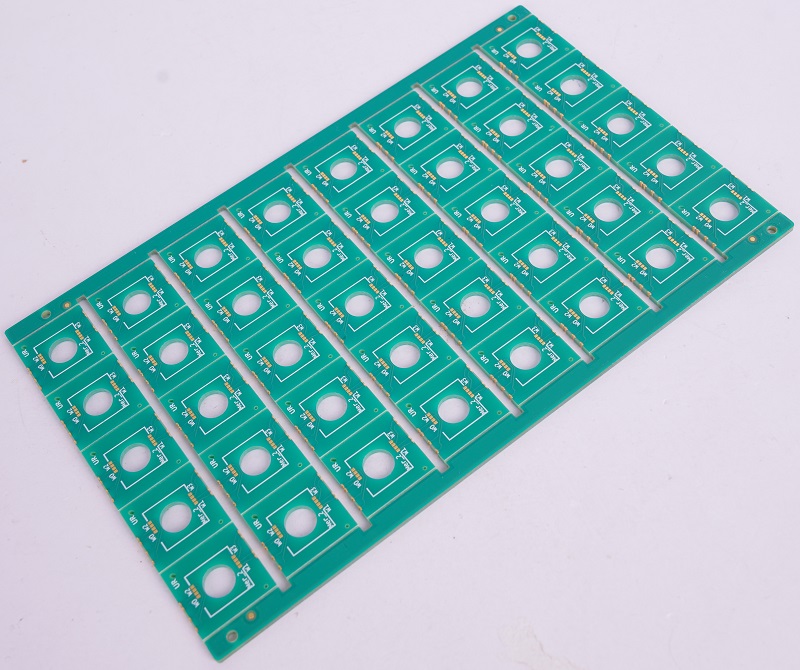
PCB panelization is a critical step in the manufacturing process that directly impacts production efficiency, material waste, and overall costs. Poor panel design can lead to lower yields, increased scrap, and delays in assembly. In this blog, we’ll explore actionable strategies to optimize PCB panelization for higher yield and cost savings.
Why Panelization Matters in PCB Manufacturing?
Panelization refers to arranging multiple PCB designs onto a single manufacturing panel (or “array”) for batch processing. Key benefits include:
Reduced material waste: Maximizing panel space utilization.
Faster assembly: Enabling automated pick-and-place machines to process multiple boards simultaneously.
Lower handling costs: Fewer individual boards to manage during fabrication and assembly.
However, suboptimal panelization can lead to:
Warpage during soldering.
V-score or routing errors.
Increased breakage during depaneling.
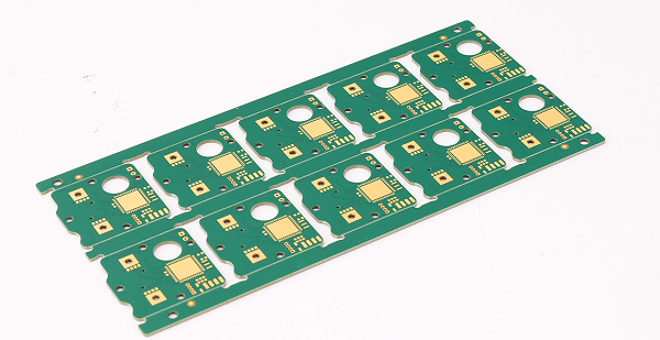
6 Tips to Optimize PCB Panelization
Base on our 19+years experiences in the PCB manufacturing field, today I would like to share you 6 Strategies to Optimize PCB Panelization
1. Choose the Right Panel Size
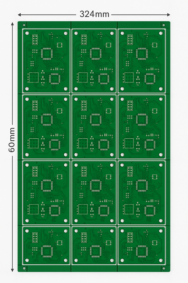
Align your PCB dimensions with standard panel sizes (e.g., 18″x24″, 21″x24″) to minimize material trimming.
Example: If your board is 80mm x 60mm, arrange 4×6 units on a 324mm x 480mm panel to reduce unused space.
2. Optimize Board Arrangement
Rotation: Rotate boards to fit more units per panel.
Mirroring: Use symmetrical designs to avoid “wasted” gaps.
Nesting software: Leverage tools like CAM350 to automate optimal layout generation.
3. Select the Best Depaneling Method
The choice of depaneling (separating individual boards) affects yield and edge quality:
V-Score: Low cost and fast, but requires straight edges and may weaken boards.
Tab Routing: Ideal for irregular shapes but adds milling time.
Laser Cutting: Precision for high-density designs, but higher cost.
Rule of thumb: Use V-score for rectangular boards and routing for complex shapes.
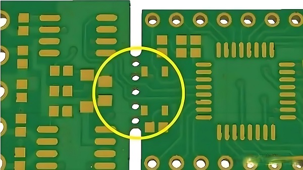
4. Add Breakaway Tabs and Mouse Bites
Breakaway tabs: Small connectors between boards to prevent movement during assembly.
Mouse bites: Perforated holes for easy manual separation.
Spacing: Maintain 1.5–2mm between boards to avoid solder mask bridging.
5. Incorporate Fiducials and Tooling Holes
Add global fiducials to the panel for accurate alignment during SMT assembly.
Include tooling holes (3.2mm diameter) to secure the panel during drilling and routing.
6. Balance Quantity vs. Risk
Overcrowding panels increases the risk of cross-board defects.
Underutilizing panels raises material costs.
Recommended: Aim for 4–20 boards per panel, depending on size and complexity.
Case Study: Cost Savings Through Smart Panelization
A consumer electronics manufacturer redesigned their 50mm x 50mm IoT module panel:
Initial design: 8 boards/panel with 15% wasted space.
Optimized design: 12 boards/panel using rotated layouts and shared tooling holes.
Results:
15% reduction in material costs.
10% faster SMT assembly.
Fewer depaneling errors due to improved tab routing.
Common Panelization Mistakes to Avoid
Ignoring manufacturer capabilities: Always consult your PCB fab’s panel size and tolerances.
Overcomplicating shapes: Complex panels increase milling time and scrap rates.
Skipping test coupons: Include test patterns for impedance control and quality checks.
Conclusion
Optimizing PCB panelization requires a balance of geometric efficiency, process knowledge, and collaboration with manufacturers. By implementing these strategies, you can reduce waste, improve yields, and lower production costs without compromising quality.
Pro Tip: Use panelization-specific design rules in tools like Altium or KiCad to automate compliance checks.
Also, if you want to know more about how to optimize PCB Panelization for Higher Yield and Lower Cost, please feel free to inquiry from us.
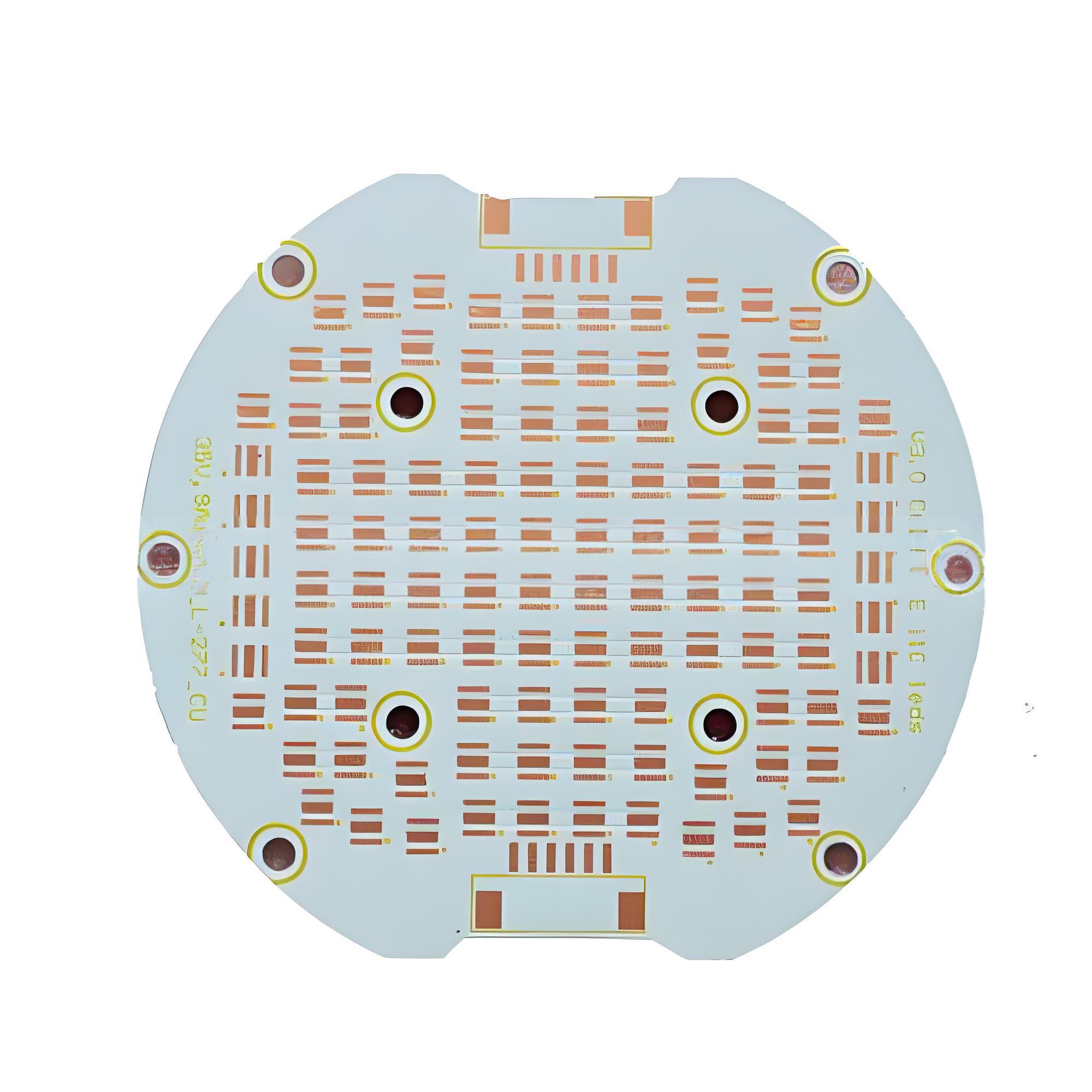
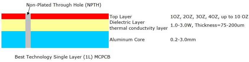
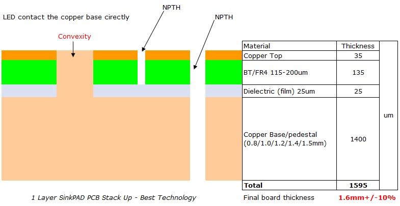
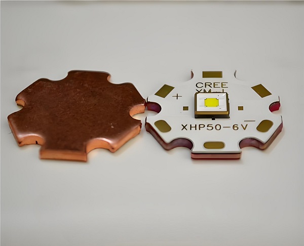
SinkPAD MCPCB is a special kind of metal core printed circuit board designed for excellent heat dissipation. It’s different from regular MCPCBs because it removes one major barrier—the insulating dielectric layer under the LED.
In simple terms, it allows heat to flow directly from the LED chip to the metal base. That means less heat build-up, more efficiency, and longer lifespan for your components.
You’ll often find SinkPAD MCPCBs in high-power LED applications—like automotive lighting, industrial lamps, medical equipment, and even UV curing systems. These are places where heat control isn’t just helpful—it’s essential.
Advantages of Sinkpad MCPCB
1. Direct Heat Flow
With no dielectric between the LED and metal core, SinkPAD boards offer a direct thermal path, reducing resistance and increasing efficiency.
2. Lower Operating Temperatures
By improving heat transfer, components stay cooler. For LEDs, this means stable brightness and a longer working life.
3. Consistent Light Output
Temperature spikes can dim or discolor LEDs. SinkPAD keeps the junction temperature stable, maintaining consistent color and brightness.
4. Compact Design
Thanks to better heat handling, you can reduce or eliminate bulky heatsinks, helping make designs smaller and lighter.
5. Durability in Harsh Conditions
SinkPAD boards resist thermal cycling, shock, and vibration, making them perfect for tough environments like aerospace or outdoor lighting.
So if your design involves powerful LEDs or components that get hot fast, this type of board can be a game-changer.
Base Materials of Sinkpad MCPCB
SinkPAD boards come with different base metals. Each one has its own strengths depending on your project.
Aluminum Core Sinkpad PCB
Aluminum is the more common choice. It’s lightweight, easy to work with, and keeps costs low. Its thermal conductivity is good—usually around 150-200 W/m·K. For applications where heat output isn’t extreme, aluminum SinkPAD PCBs are a great fit. You’ll find them in general LED lighting, backlit signs, and other consumer electronics.
They’re also a smart option if you’re trying to keep your SinkPAD MCPCB price in check. But actually, for consumer electronics, conventional metal core PCB can cover it.
Copper Core Sinkpad PCB
Copper is all about performance. It has much higher thermal conductivity—around 385-400 W/m·K—which means it can handle intense heat. If your LEDs are pushing a lot of power or operating in a hot environment, copper is the better option. Some industrial like UV lights, high-performance lasers, or automotive headlights that stay on for long hours.
Copper boards are heavier and more expensive than aluminum ones, but they deliver top-tier thermal results.
How Does Sinkpad MCPCB Work?
In a standard MCPCB, the LED sits on a copper trace. Under that trace is a dielectric layer. Below that is the metal core, its structure just like below. Heat has to travel through all of this to get out. That creates resistance.
However, sinkPAD skips the dielectric layer—at least under the LED’s thermal pad. Instead, the heat flows straight from the LED’s thermal pad into a thermal cavity that connects directly to the base metal. This structure is often called a Direct Thermal Path (DTP).
It’s like giving heat a shortcut out of the system. No extra layers. No slowdowns. Just fast, efficient cooling. This design improves overall thermal conductivity and gives you tighter control over junction temperatures.
Thermal Conductivity of Sinkpad MCPCB
Thermal conductivity is key when you’re dealing with LEDs and power electronics. The better the board can spread heat, the better your device performs.
With aluminum cores, you’ll typically see thermal conductivity in the 150–200 W/m·K range. That’s solid for most LED needs. With copper cores, you’ll reach up to 400 W/m·K, giving you elite heat handling.
Sinkpad MCPCB vs. Conventional MCPCB
So what are the differences between sinkpad metal core PCB and traditional metal core PCB? Here we made a comparison between them:
Property
SinkPAD MCPCB
Conventional MCPCB
Heat Transfer
Direct path (through convexity pad)
Through dielectric
Thermal conductivity
Up to 400W/m.k
Up to 8W/m.k
Thermal Resistance
0.4°C/W or lower
1.0–2.0°C/W
Light Stability
High (because most use copper)
Medium
LED Lifespan
Extended
Shorter under heat
Space Needed
No
Larger cooling required
Cost
Slightly higher
Lower upfront
SinkPAD boards give better performance and better results—especially when heat control is non-negotiable. They cost more, but what you get in return is worth it in critical applications.
Considerations When Using Sinkpad MCPCB
SinkPAD MCPCBs aren’t plug-and-play for every project. There are a few things you’ll want to keep in mind before designing with them.
1. Know Your Heat Load
If your LEDs don’t generate much heat, you might not need SinkPAD. But if your design involves high wattage, tight spaces, or long run times—then yes, it’s worth considering.
2. Choose the Right Core
Use aluminum if your budget is tight or if weight is a concern. Go with copper when you need every ounce of thermal performance you can get.
3. Plan for Heatsinks
Even though the board transfers heat well, it still needs a place to send that heat. Match your SinkPAD PCB with a proper heatsink or thermal interface.
4. Soldering Profiles
Because these boards transfer heat so quickly, your reflow or wave soldering profile might need to be adjusted. Too much heat too fast can be a problem.
5. Work With an Experienced Supplier
Not all board suppliers are familiar with SinkPAD technology. Make sure your manufacturer knows how to handle the convexity design and machining process correctly. If you are searching for a reliable sinkpad MCPCB manufacturer, do not miss out EBest Circuit (Best Technology). We have over 18 years experiences, and we have experienced engineers and operators to give you a high quality sinkpad copper core PCB.
How Does the Cost of Sinkpad MCPCB Compare to Conventional MCPCB?
So, how does the cost of sinkpad MCPCB compare to the conventional MCPCB? Actually, the price of sinkpad PCB is higher than that of a standard MCPCB. Because the process is more complex. There’s more precision involved in removing the dielectric under the LED. And if you’re using copper, that adds more to the cost.
Here’s what influences the price:
Core material (aluminum vs. copper)
Board size and thickness
Layer count
Volume of your order
Custom thermal pad design
But here’s the real question: does it save you money in the long run? For many, the answer is yes. Here’s why:
You don’t need oversized heatsinks
Your LEDs last longer
Fewer failures mean lower service costs
Your product performs better, with fewer returns
When you weigh the total system cost—not just the board—the extra investment often pays off.
SinkPAD MCPCBs offer a smart solution for thermal challenges in LED and power electronics. They bring something special to the table—direct heat transfer from the source to the metal base.
If your design involves strong heat loads, tight spaces, or critical reliability, this is the kind of PCB that can make a difference. In our next blog, we will share the factors affect the cost of sinkpad PCB. If you want to know more about sinkpad PCB, you are welcome to contact us at any time.
FAQs
1. What makes Sinkpad MCPCB more effective than a standard MCPCB?
It creates a direct path from the LED to the metal core, removing the thermal barrier and increasing heat flow.
2. Can I use aluminum Sinkpad MCPCB for high-power LEDs?
Yes, if thermal output is moderate. For extreme power or heat, copper may perform better.
3. Does it support double-layer designs?
Sinkpad technology is usually single-sided due to its thermal cavity, but custom options are available.
4. Is the cost justified in consumer products?
In mid- to high-end products where longevity and brightness matter, yes. It reduces long-term failures and service needs.
5. How do I choose between aluminum and copper Sinkpad cores?
Look at the application. If weight and cost are more critical, aluminum works well. For demanding environments, copper is better.
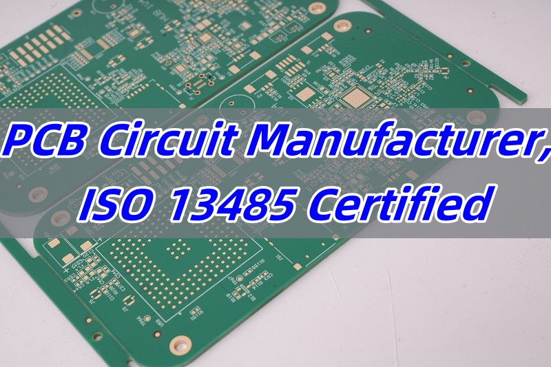
A PCB circuit manufacturer is the driving force behind the production of printed circuit boards (PCBs), which are the heart of countless electronic devices. In this blog, we’ll dig deep into various aspects related to PCB circuit manufacturers, from identifying the best ones to understanding how to choose the right partner for your needs.
As an ISO 13485 certified manufacturer, EBest Circuit (Best Technology) offers assorted PCB solutions to the domestic and international markets. Quality is the anchor that EBest Circuit (Best Technology) can build rapport with customers. We pay attention to the production effectiveness and the core benefits of customers. In EBest Circuit (Best Technology), our engineers excel in DFM analysis, PCB circuit design, component sourcing, production process improvement, technical support, and quality control. If any new demand about FR4, ceramic PCB, MCPCB, or PCB assembly, kindly contact us at sales@bestpcbs.com for support.
What is the best PCB circuit manufacturer?
Determining the best PCB circuit manufacturer depends on several factors. Quality, reliability, and cost effectiveness are key considerations.
Quality-Focused Manufacturers: Some manufacturers are known for their high-quality standards. They use advanced manufacturing techniques and strict quality control processes. For example, companies that follow ISO 9001 and IPC standards ensure that their PCBs meet international quality benchmarks.
Innovation-Driven Firms: Others stand out for their innovative approach. They are constantly researching and developing new technologies to improve the performance and functionality of PCBs. These manufacturers are often at the forefront of producing PCBs for emerging industries like artificial intelligence and the Internet of Things (IoT).
Cost-Efficient Options: There are also manufacturers that offer a good balance between quality and cost. They can provide cost effective solutions without compromising on the basic requirements of the PCBs. This is especially important for small and medium-sized enterprises (SMEs) with budget constraints.
Who manufactures PCB circuit?
EBest Circuit (Best Technology) is an ISO 13485 certified PCB circuit manufacturer. We have advanced production facilities and a global presence. We can handle from low-volume to large-volume orders. The mouthy capability in EBest Circuit (Best Technology) is 260,000 square feet (28,900 square meters).
Apart from the traditional PCBs, we also focus on special PCBs, such as high-frequency PCBs for telecommunications, bus bar PCBs for automotive and aerospace applications. Rapid PCB prototyping and high-quality PCB manufacturing are our assets, especially for small-scale projects or when quick turnaround times are needed. We can offer personalized service and faster delivery compared to some larger-scale manufacturers.
Who is the largest PCB circuit manufacturer in the world?
As of recent times, several companies compete for the title of the largest PCB circuit manufacturer.
TTM Technologies: It is a well-known global player. With manufacturing facilities in multiple countries, TTM Technologies has the capacity to produce a large volume of PCBs. They serve a wide range of industries, including aerospace, defense, and telecommunications.
Unimicron Technology Corporation: Based in Taiwan, Unimicron is another major manufacturer. They have a significant market share in the global PCB industry and are known for their advanced manufacturing capabilities and high-quality products.
Zhen Ding Technology Holding Limited: This Chinese company has grown rapidly in recent years. It has large scale production facilities and a strong R & D team, enabling it to produce a vast number of PCBs for various applications.
Top PCB circuit manufacturers in USA
The United States has some top notch PCB circuit manufacturers.
Sanmina Corporation: Sanmina offers a comprehensive range of PCB manufacturing services. They have state-of-the-art facilities and a team of experienced engineers. Their products are used in industries such as medical, industrial, and telecommunications.
Advanced Circuits: Known for its quick-turn PCB services, Advanced Circuits is a popular choice among customers who need fast prototyping. They have a user-friendly online platform that allows customers to easily place orders and track the progress of their PCBs.
TTM Technologies (USA Operations): In addition to its global presence, TTM’s US operations are significant. They can produce high-complexity PCBs with high precision, making them suitable for high-end applications like military and aerospace.
Online Search: Use search engines to look for PCB circuit manufacturers. You can filter your search by location, type of PCBs they produce, and customer reviews. Many manufacturers also have their own websites where you can learn more about their services and products.
Industry Directories: There are industry specific directories that list PCB circuit manufacturers. These directories often provide detailed information about the companies, including their capabilities, certifications, and contact details.
Referrals: Ask for recommendations from colleagues, business partners, or other professionals in the electronics industry. Word-of-mouth referrals can be a great way to find reliable manufacturers.
Trade Shows: Attend electronics trade shows and exhibitions. This is a great opportunity to meet manufacturers in person, see their products, and discuss your requirements directly with them.
How to choose a PCB circuit manufacturer?
Choosing the right PCB circuit manufacturer is essential for the success of your project. Here are some factors to consider:
Quality Standards: Look for manufacturers that follow strict quality control processes. Check if they have relevant certifications such as ISO 9001 and IPC standards. A manufacturer with high-quality standards is more likely to produce reliable PCBs.
Technical Capabilities: Consider the manufacturer’s technical capabilities. Can they produce the type of PCBs you need, such as multi-layer PCBs or high-frequency PCBs? Do they have the necessary equipment and expertise to handle your project?
Cost: Cost is an important factor, but it shouldn’t be the only one. Compare the prices of different manufacturers, but also consider the quality and service they offer. Sometimes, paying a little more for a higher-quality PCB can save you money in the long run.
Turnaround Time: If you have a tight deadline, choose a manufacturer that can offer a fast turnaround time. Some manufacturers specialize in quick-turn PCBs and can deliver your order in a short period.
Customer Service: Good customer service is crucial. A manufacturer that is responsive to your inquiries and provides support throughout the manufacturing process can make your experience much smoother.
Why should you choose EBest Circuit (Best Technology) as your trusted PCB circuit manufacturer?
Superior Quality: EBest Circuit (Best Technology) adheres to the highest quality standards. Their PCBs undergo rigorous testing at every stage of the manufacturing process. This ensures that the final products are reliable and meet or exceed your expectations.
Advanced Technology: The company invests in the latest manufacturing technologies. They use advanced equipment and techniques to produce PCBs with high precision and efficiency. This allows them to handle complex projects and produce innovative PCB designs.
Customization: EBest Circuit (Best Technology) understands that every customer has unique requirements. They offer customized PCB solutions, from the initial design to the final production. Their experienced engineering team can work closely with you to develop PCBs that are tailored to your specific needs.
Fast Turnaround: In today’s fast-paced market, time is of the essence. EBest Circuit (Best Technology) has a streamlined production process that enables them to deliver PCBs quickly. Whether you need a prototype or a large scale production order, they can meet your deadlines.
Excellent Customer Support: Their customer support team is always ready to assist you. They are available to answer your questions, provide technical advice, and ensure that your project runs smoothly from start to finish.
In conclusion, the world of PCB circuit manufacturers is diverse and full of options. By understanding the different aspects of choosing a manufacturer, from identifying the best ones to evaluating their capabilities, you can make an informed decision. And if you’re looking for a reliable partner, EBest Circuit (Best Technology) offers a combination of quality, technology, and excellent service that makes it a top choice. Kindly contact us at sales@bestpcbs.com for the PCB circuit technical support.
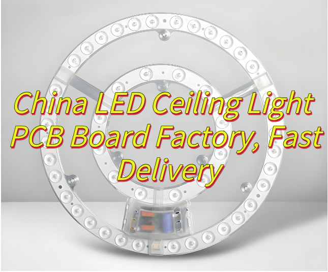
Why choose LED ceiling light PCBboard? This guide covers definition, components, functions, factory selection, fast delivery solutions, and safe replacement methods.
When you need high qualityLED ceiling light PCB board with unbeatable value, EBest Circuit (Best Technology) stands out as your ideal China-based manufacturer. We offer factory-direct pricing—cutting out middlemen to save you 20-30% on costs while maintaining stringent IPC Class 2/3 standards. With in-house production and vertically integrated supply chains, we guarantee fast 15-day bulk order delivery—50% quicker than industry averages. Need samples to test? Our 24-hour rapid prototype service ensures functional boards reach your lab within 1 working day for standard designs, keeping your projects on track. Backed by 10+ years of OEM/ODM expertise, we provide UL/CE/RoHS-certified solutions with lifetime technical support. Whether you need aluminum-core, high-CRI, or dimmable PCBs, we deliver reliability at speed. Contact us today if you have any request for LED ceiling light PCB board: sales@bestpcbs.com.
What Is LED Ceiling Light PCB Board?
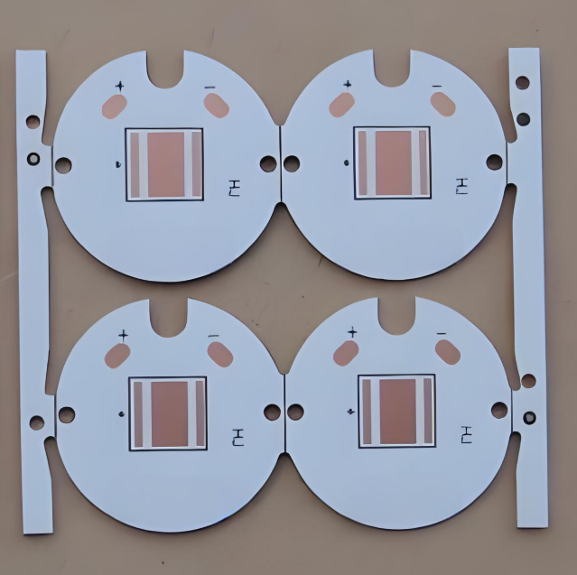
The LED ceiling light PCB boardserves as the structural and electrical foundation for modern ceiling-mounted lighting systems. This printed circuit board integrates multiple LED chips, power drivers, and thermal management components into a unified platform, enabling efficient light emission while ensuring stable operation. The LED ceiling light PCB board typically features aluminum or FR4 substrates to balance heat dissipation and circuit reliability. Its design accommodates various lighting layouts, from simple circular patterns to complex multi-zone configurations, making it adaptable for residential, commercial, and industrial applications. With optimized trace routing and component placement, the LED ceiling light PCB Board maximizes energy efficiency and longevity, often supporting dimming protocols and smart control interfaces. Proper thermal vias and copper layers in the LED ceiling light PCB Board prevent overheating, maintaining consistent brightness over extended periods.
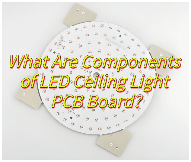
What Are Components of LED Ceiling Light PCB Board?
Components of LED ceiling light PCB board:
Base Substrate Material: The foundation of an LED ceiling light PCB board is its substrate, typically made from FR-4 (glass-reinforced epoxy), aluminum, or ceramic. FR-4 is chosen for cost efficiency in standard lighting applications, while aluminum excels in thermal management for high-power LEDs. Ceramic substrates are reserved for premium designs demanding superior heat dissipation and electrical insulation properties.
Conductive Circuitry: Copper foil traces form the electrical pathways, with a minimum thickness of 35 micrometers to ensure low resistance and efficient current flow. These traces are precisely etched using advanced manufacturing techniques to maintain signal integrity and minimize energy loss during operation.
LED Mounting Pads: Metallized pads, usually copper with surface finishes like HASL (lead-free), ENIG, or OSP, serve as attachment points for LED chips. Their layout is carefully designed to accommodate the thermal expansion characteristics of LED packages, preventing solder joint fatigue over extended use.
Thermal Management Features: To manage heat, PCBs incorporate thermal vias and copper-filled plating that conduct heat away from LED junctions. In high-power designs, dielectric polymer layers with thermal conductivity up to 3.0 W/m·K bridge the gap between LED chips and aluminum heat sinks, ensuring efficient cooling.
Electrical Components: Surface-mount devices (SMDs) include resistors, capacitors, diodes, transistors, and integrated circuits such as constant-current drivers (e.g., PT4115 with ±5% accuracy). These components are placed with high precision using automated machinery, ensuring reliable performance.
Interconnect Structures: Plated through-holes (PTHs) connect circuitry between layers in multilayer boards, while blind/buried vias reduce signal interference in high-frequency designs. Edge connectors enable modular daisy-chaining, simplifying installation in linear lighting systems.
Protective Coatings: Conformal coatings (epoxy or urethane-based) shield the board from environmental hazards, including humidity (up to 85% RH), salt spray (ASTM B117 compliance), and chemical exposure (IP65+ ratings). Selective coating processes maintain solderability while protecting critical areas.
Mechanical Anchorage: Features like press-fit brass inserts for mounting holes, alignment pins for precise optical component registration, and breakaway tabs for panelized production ensure robust mechanical integrity and ease of assembly.
Identification Markings: Laser-etched markings include part numbers, polarity indicators, certification logos (UL/CE), and QR codes linking to digital datasheets. These markings use durable ceramic-filled ink for permanent legibility.
Test Access Points: Bed-of-nails test pads enable automated in-circuit testing (ICT) for continuity verification, isolation resistance (>1GΩ), and functional testing of components. Boundary-scan architectures comply with IEEE 1149.1 standards, ensuring thorough validation of complex designs.
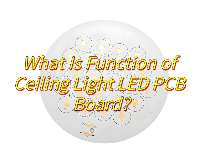
What Is Function of Ceiling Light LED PCB Board?
Function of ceiling light LED PCB board:
Power Distribution and Stability: The LED PCB board serves as the primary conductor, converting AC power to DC and distributing it evenly across multiple LED chips through precision-engineered traces. This ensures consistent brightness and prevents voltage drops, critical for maintaining uniform illumination in commercial spaces like offices or retail stores.
Thermal Management: Constructed with metal-core substrates such as aluminum, the PCB efficiently dissipates heat generated by LEDs. This design prevents thermal runaway, extending the lifespan of LED components and maintaining color consistency over extended periods, even in high-temperature environments.
Optical Integration Support: The board’s surface incorporates reflective coatings and optical-grade solder masks to enhance light output. By directing photons efficiently, it minimizes glare and maximizes luminous efficacy, essential for applications requiring precise lighting control, such as art galleries or museums.
Smart Connectivity: Modern PCB boards include embedded interfaces for IoT integration, enabling wireless control via protocols like Bluetooth or Wi-Fi. This allows dynamic adjustments to brightness, color temperature, and scheduling, aligning with smart building ecosystems for energy-efficient operations.
Structural Durability: Engineered with robust materials like FR-4 or CEM-3, the PCB withstands mechanical stress during installation and operation. Its rigid construction ensures long-term reliability, reducing maintenance needs in high-traffic areas such as airports or hospitals.
Safety Compliance: The board incorporates safety features like fuse links and insulation barriers to meet global standards (e.g., UL, IEC). These protections prevent electrical hazards, ensuring safe operation in environments with strict regulatory requirements.
Dimming Compatibility: Optimized circuitry supports advanced dimming methods, including PWM and 0-10V control, without causing flicker or color shift. This flexibility allows seamless integration with building management systems for personalized lighting experiences.
Modular Upgradeability: Standardized PCB designs facilitate easy replacement or expansion, enabling upgrades to newer technologies like Li-Fi or enhanced sensors. This adaptability protects investments by extending the functional lifespan of lighting fixtures.
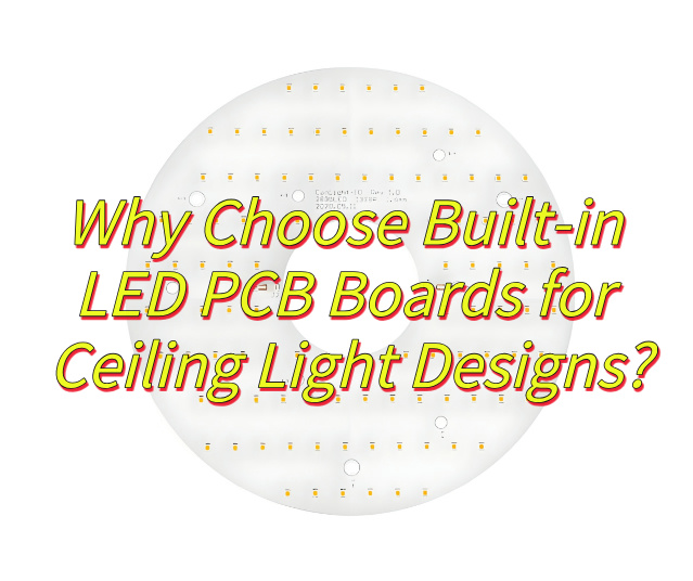
Why Choose Built-in LED PCB Boards for Ceiling Light Designs?
Here are reasons why choose built-in LED PCB boards for ceiling light designs:
Streamlined Aesthetic Integration Built-in LED PCB boards enable ultra-thin fixture profiles by eliminating external drivers, creating flush-mount designs ideal for contemporary interiors. This sleek form factor disappears into ceilings, preserving architectural lines in luxury residences or commercial spaces where visual minimalism is paramount.
Optimized Thermal Dissipation Direct bonding of PCBs to aluminum heat sinks creates a unified thermal path, reducing junction temperatures by 20–30% versus modular designs. This efficiency prevents lumen depreciation in environments like heated offices or industrial workshops, maintaining 95%+ light output over 50,000 hours.
Precision Optical Engineering Onboard microstructures—such as embedded lenses and diffusers—are factory-aligned with LED chips during SMT assembly. This calibration ensures ±5° beam accuracy and UGR <19 performance, critical for task lighting in hospitals or galleries requiring glare-free illumination.
Rapid Installation Protocols Tool-free PCB modules with push-pin connectors reduce installation time by 50% compared to traditional hardwiring. Electricians can pre-wire multiple fixtures during rough-ins, then snap boards into place for final commissioning in high-rise renovations or hotel projects.
Circuit-Level Energy Efficiency Compact PCB layouts shorten conductive pathways, cutting I²R losses by 28% according to thermal imaging studies. This allows 18W LED boards to match 25W fluorescent outputs, aligning with LEED v4.1 requirements for energy-efficient commercial lighting.
Smart Infrastructure Readiness PCB designs incorporate unused footprints for PoE+ modules or Zigbee chips, enabling future upgrades to connected lighting systems. This adaptability future-proofs investments in university campuses or corporate HQs planning IoT deployments.
Harsh Environment Resistance Conformal coatings (IPC-CC-830B compliant) and 2.5mm solder mask dam protect PCBs from corrosive agents like VOCs or salt spray. Fixtures in marine environments or swimming pools retain functionality through 1,000-hour salt fog tests per ASTM B117.
Code-Compliant Safety Architecture Double-sided insulation layers and 4mm creepage distances exceed IEC 60598-2-2 requirements for Class II construction. This design prevents electric shock risks in damp locations like bathrooms or spas, meeting NEC Article 410 stringency.
How to Evaluate A China LED Ceiling Light PCB Board Factory?
Production Certification & Compliance Verify the factory holds ISO 9001 (quality management), ISO 14001 (environmental management), and industry-specific certifications like IATF 16949 (automotive) or ISO 13485 (medical). Export-oriented products must meet RoHS (hazardous substance restrictions), REACH (chemical management), and UL (safety) standards. These certifications ensure adherence to global quality and environmental norms.
Technical Capabilities & Equipment Assess the presence of high-precision automated machinery such as SMT placers, AOI (Automated Optical Inspection), and X-ray detectors. Advanced equipment ensures soldering accuracy and defect detection. Inquire about their technical team’s expertise in handling complex processes like BGA assembly or fine-pitch component placement.
Quality Control System Evaluate welding quality metrics (e.g., solder penetration ≥75%, component deviation ≤1/4 of terminal size), visual inspections (board cleanliness, component alignment), and electrical tests (insulation resistance, voltage withstand). Environmental stress testing (thermal cycling, humidity, vibration) confirms product reliability under real-world conditions.
Supply Chain & Production Management Review material sourcing protocols to ensure raw material quality and supply stability. The production facility should maintain cleanroom standards and comply with occupational health regulations (e.g., wastewater/air treatment). Assess daily output capacity, lead times, and ability to meet rush orders, particularly during peak seasons.
Customer Service & Support Prioritize factories offering tailored solutions (e.g., circuit design optimization, material selection advice). Responsive after-sales teams for troubleshooting and repairs are critical. A robust feedback mechanism to address issues promptly reduces long-term partnership risks.
Environmental & Regulatory Compliance Confirm use of lead-free solder, waste recycling programs, and adherence to RoHS/REACH. Energy-efficient equipment and process optimizations (e.g., ISO 14001 practices) reduce ecological impact and operational costs.
Financial Stability & Reputation Analyze financial statements for profitability, cash flow, and R&D investments to gauge long-term viability. Industry reputation and client case studies provide insights into real-world performance; prioritize partners with proven success in relevant sectors.
Pricing & Delivery Competitiveness Compare quotes across suppliers while balancing quality and service. Clarify lead times (standard vs. expedited) and flexibility for urgent orders to align with project timelines.
How to Achieve Fast Delivery of LED Ceiling Light PCB Board Orders?
This is how to achieve fast delivery of LED ceiling light PCB board orders:
Optimize Supply Chain Collaboration: Partner with local or regionally aligned component suppliers to minimize lead times for materials like copper-clad laminates and LED packages. Implement real-time inventory synchronization to ensure raw materials arrive just-in-time for production, avoiding delays from stockouts or overordering.
Streamline Production Workflows: Deploy automated SMT (Surface Mount Technology) lines with adaptive scheduling systems to prioritize urgent orders. Implement cellular manufacturing layouts where PCB assembly, testing, and packaging occur in contiguous zones, reducing material handling time by up to 30%.
Maintain Strategic Buffer Stock: Hold safety stock for frequently specified PCB configurations (e.g., 2-layer 1.6mm FR-4 boards with 1oz copper). Use predictive analytics based on historical order patterns to replenish buffer inventory without incurring excessive carrying costs.
Leverage Express Logistics Networks: Pre-negotiate contracts with multiple couriers for expedited air freight options. For time-sensitive domestic deliveries, utilize dedicated last-mile delivery services with GPS tracking to ensure 24-hour turnaround from factory to customer.
Implement Digital Order Management: Adopt cloud-based platforms enabling customers to self-submit orders with BOM (Bill of Materials) files and receive instant DFM (Design for Manufacturability) feedback. Automated order confirmation emails with production timelines reduce back-and-forth communication delays.
Accelerate Quality Validation: Integrate in-line AOI (Automated Optical Inspection) and ICT (In-Circuit Test) systems to complete 100% functional testing in <2 minutes per board. Implement statistical process control charts to identify and correct process deviations in real time, preventing batch rework.
Design for Rapid Manufacturability: Encourage customers to adopt standardized board sizes and common component footprints during the design phase. Offer free DRC (Design Rule Check) services to identify potential production bottlenecks before fabrication begins.
Establish Contingency Production Lines: Maintain dedicated “express lanes” with isolated equipment and skilled operators for rush orders. These lines bypass standard production queues, ensuring 48-hour turnaround for simple PCB designs without disrupting ongoing larger projects.
Pre-Clear Customs Documentation: For international shipments, prepare export declarations and certificate of origin documents in parallel with production. Collaborate with customs brokers to secure AEO (Authorized Economic Operator) status, reducing clearance time by 40% at ports.
Post-Production Aggregation Strategy: Consolidate completed orders from multiple clients into full container loads for ocean freight where possible, balancing cost and speed. For air shipments, use pre-packed reusable crates to eliminate loading delays at the dock.
How to Replace A LED Ceiling Light PCB Board Safely?
Here are how to replace a LED ceiling light PCB board safely:
Power Disconnection Protocol: Begin by turning off the circuit breaker supplying power to the ceiling light. Use a non-contact voltage tester to confirm zero electrical potential at the fixture terminals. For added safety, place a warning sign on the electrical panel to prevent accidental reactivation during maintenance.
Fixture Deconstruction: Remove the decorative diffuser or lens by gently rotating counterclockwise or releasing spring-loaded clips. Unscrew retaining bolts securing the LED module using an insulated screwdriver. Support the PCB assembly during removal to prevent accidental falls or component damage.
Wiring Disconnection: Document wire connections using color photography or labeled tape before detachment. Use needle-nose pliers to release spade terminals or IDC connectors. For soldered connections, apply controlled heat with a temperature-controlled soldering station (280–320°C) to avoid thermal shock to adjacent components.
PCB Inspection Protocol: Visually examine the old board for signs of overheating (discoloration, solder flux residue) or mechanical stress (cracked traces). Perform continuity tests on removed components using a multimeter to identify potential reuse candidates.
New Board Preparation: Pre-bend component leads on the replacement PCB only if necessary for assembly. Apply a thin layer of heatsink compound to thermal pads if specified in the product documentation. Avoid touching conductive areas to prevent electrostatic discharge (ESD) damage.
Reassembly Sequence: Mount the new PCB using original hardware, ensuring proper alignment with optical components (lenses, reflectors). Torque screws to manufacturer specifications (typically 0.6–0.8 Nm) using a calibrated torque screwdriver. Reconnect wires following the documented color code or labeling.
Functional Verification: Restore power temporarily to test LED operation before finalizing installation. Confirm correct color temperature (measured with a spectrometer if available) and beam angle consistency. Check for flicker using smartphone camera slow-motion mode.
Final Assembly: Reattach the diffuser, ensuring proper seating to maintain IP rating (if applicable). Clean the fixture surface with isopropyl alcohol and a lint-free cloth to remove fingerprints or debris. Dispose of old PCBs through certified e-waste recyclers.
Documentation Update: Record the replacement date, PCB revision, and component lot numbers in the facility maintenance log. This creates an audit trail for warranty claims and facilitates troubleshooting in future service calls.
Post-Installation Monitoring: Observe the fixture for 24–48 hours to detect early failures. Monitor junction temperatures with an infrared thermometer (target <85°C for aluminum-backed PCBs). Schedule follow-up inspections at 6-month intervals for critical installations.
How to Get Fast Delivery from China LED Ceiling Light PCB Board Factories?
This is how to get fast delivery from China LED ceiling light PCB board factories:
Leverage Localized Supply Chains: Partner with factories that source components regionally to minimize lead times for materials like copper-clad laminates and LED packages. Prioritize suppliers with established relationships with nearby logistics hubs for faster material procurement.
Implement Agile Production Systems: Choose manufacturers using automated SMT lines with dynamic scheduling capabilities to prioritize urgent orders. Choose factories employing cellular manufacturing layouts, which reduce material handling time by grouping assembly, testing, and packaging in contiguous zones.
Maintain Strategic Buffer Stock: Work with suppliers to hold safety stock for commonly specified PCB configurations (e.g., 2-layer 1.6mm FR-4 boards with 1oz copper). Utilize predictive analytics based on historical order data to replenish inventory without incurring excessive storage costs.
Utilize Express Logistics Solutions: Pre-negotiate contracts with multiple couriers for expedited air freight options. For domestic deliveries, engage dedicated last-mile services with real-time GPS tracking to ensure 24-hour turnaround from factory to destination.
Adopt Digital Order Platforms: Select factories offering cloud-based systems for instant order submission, DFM (Design for Manufacturability) feedback, and automated order confirmation emails with production timelines. This reduces communication delays and accelerates order processing.
Accelerate Quality Assurance: Choose suppliers with in-line AOI (Automated Optical Inspection) and ICT (In-Circuit Test) systems that complete 100% functional testing in under 2 minutes per board. Statistical process control charts help identify and correct deviations in real time, preventing batch rework.
Encourage Standardized Designs: Advocate for standardized board sizes and common component footprints during the design phase. Factories often provide free DRC (Design Rule Check) services to identify potential production bottlenecks before fabrication begins.
Establish Dedicated Express Lines: Select manufacturers maintaining isolated “express lanes” with dedicated equipment and operators for rush orders. These lines bypass standard production queues, ensuring 48-hour turnaround for simple PCB designs without disrupting larger projects.
Pre-Clear Customs Documentation: For international shipments, ensure export declarations and certificates of origin are prepared in parallel with production. Collaborate with customs brokers holding AEO (Authorized Economic Operator) status to reduce clearance time by up to 40% at ports.
Consolidate Shipments Strategically: Aggregate completed orders from multiple clients into full container loads for ocean freight where feasible. For air shipments, use pre-packed reusable crates to minimize loading delays at the dock, balancing cost and speed effectively.
Conclusion
In conclusion, for reliable LED ceiling light PCB boards with superior performance and fast delivery, EBest Circuit (Best Technology) stands as your trusted China factory partner offering factory-direct prices and 24-hour sample service. Contact us today for a competitive quote on your next lighting project.
A printed circuit manufacturer is the backbone of the electronics world. They are the ones who transform the theoretical designs of printed circuit boards (PCBs) into tangible, functional components that power our devices. From the smartphones in our pockets to the complex machinery in factories, PCBs are everywhere, and the manufacturers behind them are the unsung heroes.
As a well-established printed circuit manufacturer, EBest Circuit (Best Technology) has about 10 engineers in the R&D department and about 20 engineers in the quality department. Most of our engineers have worked at EBest Circuit (Best Technology) for over 10 years, who know the ropes and have solved the assorted PCB cases for over 1700 customers across 40 countries. We are committed to providing the turnkey electronic circuit solution to global customers. Your trust is our invaluable treasure. If you have any printed circuit projects, warm welcome to contact us at sales@bestpcbs.com. Looking forward to getting your inquiries soon.
Who is Printed Circuit Manufacturer in China?
China has emerged as a global powerhouse in the field of printed circuit manufacturing. There are several well-known manufacturers in the country that have earned a reputation for quality and efficiency.
EBest Circuit (Best Technology)
EBest Circuit (Best Technology) is highly regarded for our advanced production technology. We have a factory and a professional R & D team. We can handle a wide range of PCB orders, from small-batch prototypes to large-scale mass production. EBest Circuit (Best Technology) has a comprehensive production system, covering everything from raw material procurement to the final product. Moreover, you not only get the final products, but you also get the solution for assorted PCBs. Our PCBs are known for the high reliability and stability, making us a popular choice for many international clients.
TTM Technologies
TTM has a significant presence in China. They focus on providing high-end PCB solutions. With a strong emphasis on innovation, they are constantly developing new technologies to meet the evolving needs of the electronics industry.
Top Printed Circuit Manufacturers in USA
The United States also has a number of top-notch printed circuit manufacturers. These companies are known for their high-quality products and strict adherence to industry standards.
Sanmina Corporation
Sanmina is a global electronics manufacturing services company with a strong focus on printed circuit manufacturing. They offer a wide range of services, including PCB design, assembly, and testing. Their products are used in various industries, such as medical, industrial, and telecommunications. They have a reputation for delivering high-quality products on time.
Celestica Inc.
Celestica is another well-known printed circuit manufacturer in the US. They provide end to end solutions for PCB manufacturing, from concept to production. They have a global network of manufacturing facilities, which allows them to serve customers around the world. Their products are used in a variety of industries, including automotive, consumer electronics, and energy.
Printed Circuit Manufacturers in India
India’s printed circuit manufacturing industry has been growing steadily in recent years. There are several manufacturers that are making a mark in the global market.
Kaynes Technology India Limited
Kaynes is a leading PCB manufacturer in India. They have a modern manufacturing facility and a team of skilled technicians. They offer a wide range of PCB products, including single-sided, double-sided, and multi-layer PCBs. Their products are used in industries such as automotive, healthcare, and telecommunications.
Moser Baer India Limited
Moser Baer is a diversified company with a significant presence in the printed circuit manufacturing sector. They have a focus on research and development, which allows them to produce innovative PCB solutions.
Pratibha Industries Limited
Pratibha Industries is involved in the manufacturing of PCBs as well as other electronic components. They have a strong commitment to quality control and use advanced manufacturing processes. Their products are used in various industries, including consumer electronics and industrial automation.
What is Printed Circuit Board Manufacturing?
Printed circuit board manufacturing is the process of creating PCBs, which are essential components in almost all electronic devices. A PCB is a board made of insulating material with conductive pathways etched or printed on it. These pathways connect different electronic components, such as resistors, capacitors, and integrated circuits, allowing them to work together as a single unit.
The manufacturing process involves several steps, from the initial design to the final testing. It requires a combination of technical expertise, advanced machinery, and strict quality control measures. The goal is to produce PCBs that are reliable, durable, and meet the specific requirements of the end-user.
What Materials are Commonly Used to Manufacture Printed Circuit Boards?
1. **Substrate Materials**
– **FR-4**: This is the most commonly used substrate material for PCBs. It is a glass fiber reinforced epoxy laminate. FR-4 is known for its good mechanical and electrical properties, as well as its relatively low cost. It can withstand high temperatures and is resistant to moisture, making it suitable for a wide range of applications.
– **Polyimide**: Polyimide is a high-performance substrate material. It has excellent thermal stability, chemical resistance, and flexibility. Polyimide-based PCBs are often used in applications where high-temperature resistance and flexibility are required, such as in aerospace and flexible electronics.
2. **Conductive Materials**
– **Copper**: Copper is the primary conductive material used in PCBs. It has high electrical conductivity, which allows for efficient transmission of electrical signals. Copper is usually applied to the substrate in the form of a thin layer, either through electroplating or lamination.
– **Gold**: Gold is sometimes used as a plating material on the contacts of PCBs. It has excellent corrosion resistance and low contact resistance, which ensures reliable electrical connections. Gold-plated contacts are commonly used in high-end applications such as military and aerospace.
3. **Solder Mask**
– Solder mask is a layer of polymer material that is applied to the PCB to protect the copper traces and prevent solder from flowing to unwanted areas during the soldering process. It is usually green in color, but other colors are also available. Solder mask helps to improve the reliability and appearance of the PCB.
4. **Silkscreen**
– Silkscreen is a layer of ink that is printed on the PCB to provide information such as component names, part numbers, and polarity markings. It helps technicians to assemble and troubleshoot the PCB more easily.
How are Printed Circuit Boards Manufactured?
**Conceptualization**: The first step is to understand the requirements of the end-product. This includes determining the number of layers, the size of the PCB, and the types of components that will be used.
**Schematic Design**: A schematic diagram is created to show the electrical connections between different components. This is a crucial step as it forms the basis for the physical layout of the PCB.
**Layout Design**: The layout design involves placing the components on the PCB and routing the conductive traces. This step requires careful consideration of factors such as signal integrity, power distribution, and thermal management.
**Substrate Preparation**: The substrate material is cut to the appropriate size and cleaned to remove any contaminants.
**Copper Deposition**: A thin layer of copper is deposited on the substrate. This can be done through electroplating or lamination.
**Photolithography**: A photoresist is applied to the copper layer, and a pattern is transferred onto it using a photomask. The exposed areas of the photoresist are then removed, leaving behind the desired copper pattern.
**Etching**: The unwanted copper is etched away, leaving only the conductive traces.
**Drilling**: Holes are drilled in the PCB to accommodate the component leads.
**Plating**: The drilled holes are plated with copper to provide electrical connections between different layers.
**Solder Mask Application**: The solder mask is applied to the PCB to protect the copper traces.
**Silkscreen Printing**: The silkscreen layer is printed on the PCB to provide component information.
**Surface Finish**: A surface finish is applied to the copper traces to prevent oxidation and improve solderability. Common surface finishes include HASL (Hot Air Solder Leveling), ENIG (Electroless Nickel Immersion Gold), and OSP (Organic Solderability Preservative).
**Electrical Testing**: The PCB is tested to ensure that all the electrical connections are working properly. This can be done using automated testing equipment.
**Functional Testing**: The assembled PCB is tested to ensure that it functions as intended in the end product.
Why Should You Choose EBest Circuit (Best Technology) as Your Trusted Printed Circuit Manufacturer?
Quality Assurance
EBest Circuit (Best Technology) has a strict quality control system in place. We follow international standards such as ISO 9001 and IPC standards. Our products undergo multiple levels of testing, from in-process inspections to final product testing. This ensures that the PCBs we produce are of the highest quality and meet the specific requirements of the customers.
Advanced Technology
The company invests heavily in research and development. We use the latest manufacturing technologies and equipment, such as high-precision drilling machines and advanced plating systems. This allows us to produce complex PCBs with high precision and efficiency.
Customization
EBest Circuit (Best Technology) understands that requirements vary from customer to customer. We offer customized solutions, from small-batch prototypes to large-scale mass production. Our experienced engineering team can work closely with customers to design and manufacture PCBs that meet their specific needs.
Fast Turnaround Time
In today’s fast-paced electronics industry, time is of the essence. EBest Circuit (Best Technology) has a streamlined production process that allows us to deliver products quickly. We can provide fast-turn prototypes within a short period, which is crucial for customers who need to test their products quickly.
Excellent Customer Service
EBest Circuit (Best Technology) has a dedicated customer service team that is available to answer customers’ questions and provide support throughout the manufacturing process. We are committed to building long-term relationships with our customers and ensuring their satisfaction.
To sum up, the world of printed circuit manufacturers is vast and diverse. Whether you are looking for a manufacturer in China, the USA, or India, there are many options available. Understanding the manufacturing process, the materials used, and the key players in the industry can help you make an informed decision.
And if you are looking for a trusted partner, EBest Circuit (Best Technology) offers a combination of quality, technology, customization, and excellent customer service that makes us a top choice. Kindly contact us at sales@bestpcbs.com for any printed circuit demands.
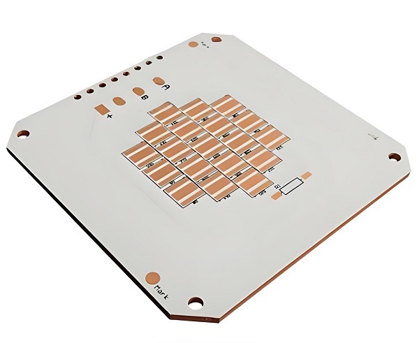
What is Thermoelectric Separation Copper Based PCB?
A thermoelectric separation copper based PCB is a special type of metal core PCB that uses thermoelectric separation technology to isolate heat and electrical pathways. Unlike traditional PCBs, this board is designed to separate heat flow from current flow, ensuring that the electronic circuit remains cooler even when high currents are running through it.
The board uses a thick copper layer to handle high current and a ceramic dielectric or polymer insulation to manage thermal conduction. This separation reduces thermal stress on components, improves reliability, and supports better performance in demanding applications such as power electronics, LED systems, and automotive electronics.
How to Distinguish Normal Copper Core PCB and Thermoelectric Separation Copper Based PCB?
1. Definition & Structure
Regular Copper-Based PCB:
This type includes a metal base, insulating layer, and circuit layer. The copper foil is usually 35μm to 280μm thick to handle high current. The insulating layer is made of alumina, silicon powder, and epoxy resin, offering good thermal resistance and elasticity.
Thermoelectric Separation Copper-Based PCB:
Uses a special process that separates the heat conduction layer from the electrical circuit layer. A copper convexity pad (heat-conductive bump) directly contacts the heat source, providing a direct heat path (zero thermal resistance). Typical structure: Circuit Layer – Convexity Pad – Insulation – Metal Base.
2. Performance Differences
Thermal Conductivity:
Regular boards rely on insulation materials (1-3W/m·K), limiting heat transfer. Thermoelectric separation boards use copper convexity (up to 400W/m·K), reducing thermal resistance by over 80% and suiting high-power applications (50–500W+).
Thermal Expansion:
Regular boards expand more with temperature, causing deformation. Thermoelectric boards have a lower coefficient of expansion.
Dimensional Stability:
Thermoelectric separation boards resist size changes better under temperature shifts, improving assembly precision.
Mechanical Strength:
Reinforced materials in thermoelectric boards provide higher strength against mechanical stress.
Electrical Properties:
Thermoelectric boards offer more stable conductivity with fewer defects like uneven resistance or noise.
3. Appearance
Regular PCB: Flat, layered, with no distinct structural features.
Thermoelectric PCB: Includes visible heat-conductive convexities (usually square or polygonal) to directly touch heat sources.
Small consumer devices (e.g., chargers, smartwatches)
Thermoelectric Separation PCBs:
Suited for high-power, high-heat devices:
High-power LED lighting (e.g., automotive headlights, industrial lamps)
Critical automotive electronics (e.g., engine control, motor drivers)
High-end electronics (e.g., LED smart TVs needing high-efficiency heat dissipation)
5. Cost & Manufacturing Complexity
Regular Copper PCBs:
Simple and cost-effective. Follows standard PCB processes: cutting, drilling, imaging, etching, solder mask, surface finish, testing, and packaging.
Thermoelectric Separation PCBs:
More complex and expensive. Requires additional steps like laser window opening, copper convexity plating, and precise insulation layering, demanding higher technical capability and manufacturing control.
Features of Thermoelectric Separation Technology
Thermoelectric separation technology brings unique benefits to metal core PCBs:
Independent Heat and Current Paths: It separates thermal conduction from electrical conduction, improving overall system stability.
Lower Thermal Resistance: Enhances the heat dissipation rate, extending the life of components.
Thicker Copper Layers: Supports high-current loads without overheating.
Stable Performance Under High Load: Useful in environments that generate intense heat.
Improved Reliability: Reduces risks of component failure due to overheating.
This advanced technology is especially important in industries where temperature sensitivity and power delivery go hand in hand, such as inverters, electric vehicles, and industrial power control systems.
Parameters of Thermoelectric Separation Metal PCB
Here are some common technical parameters for thermoelectric separation copper based PCBs:
Parameter
Value / Range
Copper Thickness
1oz to 12oz (35μm to 420μm)
Dielectric Material
Ceramic/polymer insulation
Dielectric Thickness
50μm – 200μm
Thermal Conductivity
2 – 10 W/m·K
Thermal Resistance
< 0.3 °C/W
Operating Temperature
-40°C to +150°C or more
Breakdown Voltage
> 2KV (depending on insulation material)
Surface Finish
ENIG, OSP, HASL, etc.
Layer Count
1L to 4L (usually single-layer for high power)
These parameters can be customized depending on the final application and power demands.
How to Make Thermoelectric Separation Copper Based PCB?
The manufacturing process of a thermoelectric separation copper based PCB is more complex than that of traditional metal core PCBs due to the need to incorporate a convexity pad structure that enables direct heat transfer. This approach demands high precision in material selection, layering, and processing. Below is a detailed overview of how these specialized PCBs are made:
1. Material Selection
The process begins by selecting the appropriate materials:
Copper Base Plate: A thick copper base (typically 1.0mm–3.0mm or more) is chosen for its excellent thermal conductivity.
Insulating Layer: A thin dielectric layer is applied, usually a high-performance ceramic or polymer with high breakdown voltage and thermal conductivity.
Copper Foil: A thick copper foil (ranging from 1oz to 12oz) is used for the circuit layer to support high current loads.
The materials must withstand high thermal stress and provide excellent heat conduction while ensuring electrical insulation between the circuit and the base.
2. Convexity Pad Design and Machining
The most important step in the thermoelectric separation structure is the machining of convex pads (also known as raised thermal columns):
These convex pads are precisely etched or milled from the copper base or applied using a punching or stamping technique.
The pads are aligned directly underneath heat-generating components, such as power transistors or LED chips.
Once mounted, these pads come into direct contact with the component’s thermal pad, allowing the heat to transfer directly to the copper base, bypassing the insulating layer.
This is what separates thermoelectric separation PCBs from traditional MCPCBs—the heat is not forced to travel through the entire insulating layer, significantly improving thermal response.
3. Dielectric Application and Lamination
After the copper base and convex pads are prepared:
A thin dielectric layer is applied on the areas without convex pads. This layer insulates the electrical circuit from the base but does not interfere with thermal conduction at the convex regions.
The dielectric must offer strong adhesion, high breakdown voltage, and excellent thermal conductivity.
Lamination is done under high temperature and pressure to bond the dielectric and copper foil securely to the base.
4. Circuit Imaging and Etching
Next, the circuit layer is created:
A photoresist is applied to the copper foil and exposed using UV light through a circuit pattern.
The exposed areas are etched away, leaving behind the desired copper traces for electrical conduction.
This step is similar to conventional PCB fabrication but requires high precision to ensure proper alignment with the convexity pads underneath.
5. Drilling and Plating
Drilling is done to create mounting holes and vias, but plated through-holes (PTHs) are usually minimized to maintain thermal isolation.
Non-conductive vias or filled vias may be used to reinforce mechanical strength without compromising thermal separation.
Surface plating such as ENIG, OSP, or HASL is then applied to protect the exposed copper and enhance solderability.
6. Solder Mask and Silkscreen
A solder mask is applied to protect non-soldering areas and prevent short circuits.
Silkscreen printing is used to mark components, polarity, and other indicators.
7. Thermal and Electrical Testing
Every thermoelectric separation copper based PCB undergoes strict inspection, including:
Thermal resistance testing to verify the efficiency of heat conduction through convex pads.
Hi-pot and insulation resistance tests to ensure the dielectric integrity.
AOI (Automated Optical Inspection) and electrical continuity testing to check circuit accuracy and reliability.
8. Final Assembly and Quality Control
In the final stage, boards are cut, cleaned, and inspected for flatness, surface finish, and mechanical strength. Tolerances are closely monitored because even a small misalignment in the convex pad area can impact thermal performance.
Where Can I Get a Thermoelectric Separation Copper Based PCB?
If you’re looking for reliable thermoelectric separation copper based PCBs, EBest Circuit (Best Technology) is a name you can trust.
As a certified PCB manufacturer with strong R&D capabilities, EBest Circuit (Best Technology) specializes in advanced copper-based PCBs, including those with thermoelectric separation technology. Our services cover everything from design support, prototyping, to mass production. We ensure:
High thermal reliability
Accurate copper thickness control
Custom insulation design
Advanced testing & quality assurance
We are ISO9001, ISO13485, IATF16949, and AS9100D certified, and our MES system guarantees complete traceability for every board.
Need a custom quote or sample? Reach out to our team anytime—we’re always happy to help with fast responses and professional support.
FAQ about Thermoelectric Separation
Q1: What is the purpose of thermoelectric separation in PCBs?
A: It separates heat flow and current flow, preventing overheating and enhancing the stability of power circuits.
Q2: Can thermoelectric separation PCBs handle high currents?
A: Yes, they are built with thick copper and special insulation to support high-current, high-power applications.
Q3: Are these boards more expensive than normal copper PCBs?
A: Yes, slightly. But the performance and reliability gains justify the investment for power-critical projects.
Q4: What applications use thermoelectric separation technology?
A: Power supplies, LED drivers, EV chargers, inverters, and industrial control systems.
Q5: Can EBest Circuit (Best Technology) help with design support?
A: Absolutely. We provide DFM checks, thermal simulations, and layout optimization for your specific application.
If you need high-quality thermoelectric separation copper based PCBs, EBest Circuit (Best Technology) is your go-to manufacturer. With cutting-edge production capabilities and a strong focus on thermal performance, we’re ready to help you create more efficient, reliable electronics.
Let us know what you need—we’ll take care of the rest.
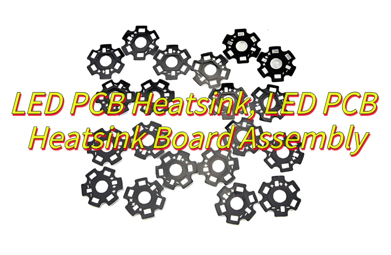
Looking for LED PCB heatsink solution? Let’s explores its definition, functions, applications, assembly processes, accuracy control, welding defect prevention, and coating consistency techniques for optimal performance.
EBest Circuit (Best Technology) excels as a premium LED PCB heatsink board assembly manufacturer by combining speed, precision, and expert support. We offer 24 hour rapid prototyping and fast-turn production, ensuring urgent projects meet tight deadlines without sacrificing quality. Equipped with fully automated SMT production lines, we guarantee high-precision assembly and rapid response to dynamic customer demands. Our dedicated engineering team provides one-on-one technical support, assisting with design optimization, thermal management solutions, and real-time troubleshooting. By leveraging advanced manufacturing and personalized expertise, we deliver high-performance, reliable LED PCB Heatsink Board Assembly tailored to your exact specifications—faster, smarter, and more efficiently than competitors. Welcome to contact us if you have any request for LED PCB assembly service: sales@bestpcbs.com.
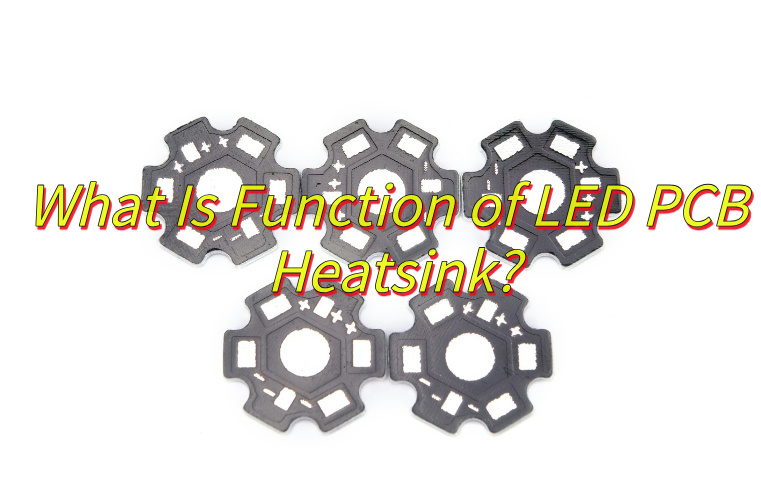
What Is LED PCB Heatsink?
LED PCB heatsink refers to a dedicated thermal management component integrated with light-emitting diode printed circuit boards to dissipate heat generated during operation. This structure typically combines a metal substrate, often aluminum or copper, with a finned or ribbed design to maximize surface area exposure to ambient air. The LED PCB Heatsink acts as a conductive pathway, transferring heat away from sensitive electronic components while maintaining operational stability. Its material selection and geometric configuration directly influence thermal efficiency, with factors like thermal conductivity coefficients and convection coefficients shaping performance. Manufacturers often machine or extrude the LED PCB Heatsink to precise tolerances, ensuring optimal contact with the PCB’s thermal pads. Proper implementation prevents overheating, which could otherwise degrade LED lifespan or cause spectral shifts. By balancing mass, surface area, and aerodynamic profiles, modern LED PCB Heatsink designs address the thermal challenges inherent in high-power lighting applications without adding excessive weight or volume to assemblies.
What Is Function of LED PCB Heatsink?
Functions of LED PCB heatsink:
Thermal Energy Dissipation: The primary role of an LED PCB heatsink is to absorb and distribute heat generated by LED chips during operation. By conducting thermal energy away from sensitive components, it prevents overheating, which could otherwise degrade LED performance or shorten lifespan.
Operational Temperature Regulation: LED PCB heatsinks maintain stable junction temperatures within safe limits, ensuring consistent light output and color accuracy. This is critical for applications like automotive headlights or studio lighting, where minor temperature fluctuations can cause visible flicker or spectral shifts.
Enhanced Thermal Conductivity: Materials like aluminum or copper alloys used in heatsinks offer high thermal conductivity, enabling rapid heat transfer from the LED die to the surrounding environment. Finned or pin-array designs further accelerate cooling through convection.
Structural Stability Support: Beyond thermal management, the heatsink provides mechanical rigidity to the LED PCB, reducing warpage caused by thermal expansion. This is particularly important for multi-layer PCBs in high-power applications like street lighting or industrial fixtures.
Corrosion and Moisture Resistance: Anodized or coated heatsink surfaces protect against environmental degradation in harsh conditions, such as marine environments or outdoor installations. This extends the service life of both the heatsink and the LED assembly.
Noise Reduction in Active Cooling Systems: In designs incorporating fans or liquid cooling, the heatsink’s geometry minimizes airflow turbulence, reducing operational noise. This makes it suitable for noise-sensitive applications like residential downlights or theater lighting.
Compatibility with Advanced LED Packages: Modern heatsinks accommodate surface-mount technology (SMT) LEDs and chip-on-board (COB) arrays through precision-machined mounting interfaces. This ensures efficient thermal coupling even in compact form factors, such as smart bulb modules.
Recyclability and Sustainability: Aluminum LED PCB heatsinks are fully recyclable, aligning with eco-design principles. Their durability also reduces electronic waste by enabling LED module reuse in retrofit projects or secondary-life applications.
What Are Applications of PCB LED Heatsink?
Applications of PCB LED heatsink:
Automotive Lighting Systems: LED PCB heatsinks enable high-power LED headlights and daytime running lights to operate reliably in extreme temperatures, ensuring consistent beam patterns and preventing premature failure due to thermal stress.
Industrial and Commercial LED Fixtures: In warehouses, factories, and retail spaces, heatsinks sustain continuous operation of high-bay lights and track lighting by managing heat buildup, reducing maintenance cycles.
Consumer Electronics Displays: TVs, monitors, and smartphones utilize miniature heatsinks to cool LED backlight units, preserving image quality and preventing screen discoloration over extended use.
Architectural and Decorative Lighting: For LED strips, wall washers, and facade lighting, heatsinks maintain aesthetic consistency by preventing color temperature shifts caused by overheating.
Medical and Surgical Lighting: Operating room lamps rely on heatsinks to stabilize LED output, ensuring surgeons have uninterrupted, shadow-free illumination during procedures.
Horticultural and Agricultural LED Grow Lights: Heatsinks support 24/7 operation of horticultural LEDs, optimizing heat dissipation to maintain photosynthetic efficiency and extend equipment lifespan.
Marine and Offshore Lighting: Corrosion-resistant heatsinks enable LED navigation lights and underwater fixtures to withstand saltwater exposure while sustaining performance.
Aerospace and Aviation Lighting: In aircraft cabin lights and exterior markers, heatsinks ensure LED reliability under extreme altitude-induced temperature fluctuations.
Entertainment and Stage Lighting: Dynamic LED stage lights and moving heads use heatsinks to prevent overheating during rapid color mixing and gobo projection cycles.
Smart Home and IoT Devices: Compact heatsinks in smart bulbs and sensors maintain LED efficiency while fitting into space-constrained, thermally challenging environments.
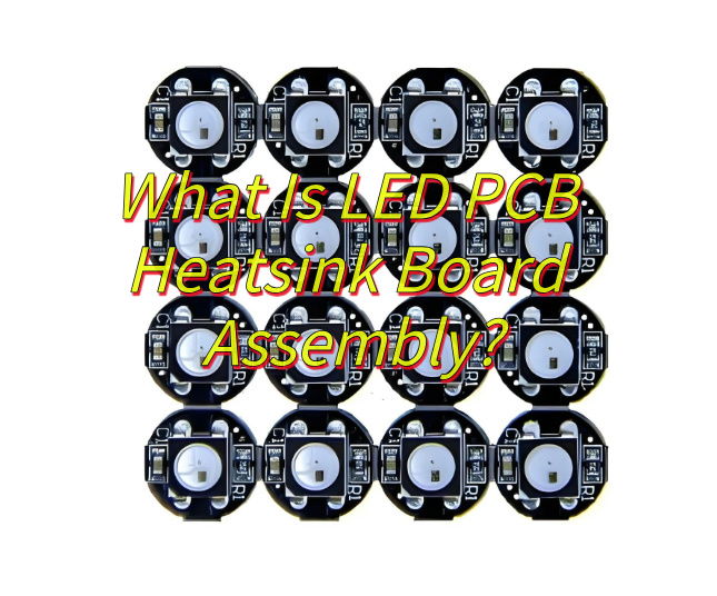
What Is LED PCB Heatsink Board Assembly?
LED PCB heatsink board assembly refers to an integrated thermal management solution combining light-emitting diode components, a metallic substrate, and specialized heat-dissipating structures. This assembly process merges the LED PCB, typically composed of aluminum or copper, with strategically engineered fins, pins, or plates to create a unified system for efficient heat transfer. During fabrication, the LED PCB heatsink board assembly undergoes precise layering of dielectric materials and copper traces to ensure electrical insulation while maintaining thermal conductivity. The design prioritizes maximizing surface area exposure to ambient air or auxiliary cooling systems, enabling rapid dissipation of heat generated by high-power LEDs. Manufacturers often employ machining, stamping, or extrusion techniques to shape the LED PCB heatsink board assembly into configurations tailored for specific form factors, from compact electronic devices to large-scale industrial fixtures. Proper execution of this assembly ensures operational stability, extends LED lifespan, and maintains optical performance by preventing thermal degradation.
What Is Process of LED PCB Heatsink Board Assembly?
Process of LED PCB Heatsink Board Assembly
Dielectric Layer Application: A thermally conductive dielectric material, such as epoxy resin or ceramic-filled polymer, is coated onto the metallic substrate. This layer ensures electrical insulation between the LED components and the heatsink while maintaining efficient heat transfer.
Circuit Layer Fabrication: Copper foil is laminated onto the dielectric layer and etched using photolithography or laser ablation to create precise conductive traces. These traces route power and control signals to the LEDs while avoiding thermal hotspots.
LED Component Mounting: Surface-mount LEDs or chip-on-board (COB) arrays are placed onto the circuit layer using automated pick-and-place machines. Solder paste or electrically conductive adhesive bonds the LEDs to the traces, ensuring both mechanical and electrical connectivity.
Heatsink Structure Formation: The metallic substrate is machined, extruded, or stamped to form fins, pins, or microchannels. These geometries maximize surface area exposure to ambient air or active cooling systems, enhancing convective heat dissipation.
Reflow Soldering or Thermal Curing: The assembly passes through a reflow oven to melt solder paste, forming permanent solder joints. For adhesive-bonded LEDs, thermal curing under controlled temperatures activates bonding agents without damaging sensitive components.
Thermal Interface Material (TIM) Integration: A layer of TIM, such as silicone-based thermal grease or graphite pads, is applied between the LED PCB heatsink board assembly and external cooling modules. This minimizes thermal resistance and ensures efficient heat path continuity.
Optical and Electrical Testing: Automated systems verify solder joint integrity, LED forward voltage, and light output consistency. Thermal imaging cameras detect hotspots, ensuring the LED PCB heatsink board assembly meets thermal performance targets.
Final Assembly and Protection: The completed assembly is integrated into lighting fixtures, with secondary optics (e.g., lenses, reflectors) added to shape light distribution. Conformal coatings or potting compounds may be applied for environmental protection in harsh settings.
How to Control the Mounting Accuracy of LED PCB Heatsink Board Assembly?
Process to control mounting accuracy of LED PCB heatsink board assembly:
Precision Tooling Design Utilize custom jigs with alignment pins and vacuum chucks to secure the LED PCB heatsink board assembly during assembly. These tools ensure positional repeatability by referencing both the PCB’s edge connectors and the heatsink’s mounting holes, minimizing deviation to ±0.03mm.
Machine Vision Alignment Deploy high-resolution cameras paired with pattern recognition software to detect fiducial markers on the PCB and heatsink. This system auto-corrects placement angles and offsets, achieving ≤0.01mm alignment accuracy for surface-mount LEDs.
Laser-Based Height Gauging Integrate spectral confocal displacement sensors to measure the Z-axis clearance between the LED PCB heatsink board assembly and optical components. This ensures planar tolerance of ±0.05mm, critical for beam uniformity in automotive headlights.
Thermal Expansion Mitigation Conduct finite element analysis (FEA) during design to simulate thermal cycling impacts. Compensate for predicted warpage by optimizing heatsink geometry or using composite materials with matched coefficients of thermal expansion (CTE).
Vacuum-Assisted Reflow Soldering Employ vacuum reflow ovens with nitrogen inerting to eliminate voids in solder joints. This reduces thermal gradients, maintaining the LED PCB heatsink board assembly’s flatness within 0.02mm across 500mm×500mm panels.
In-Line Coordinate Measurement Use portable CMM arms with touch-trigger probes to validate critical dimensions (e.g., heatsink fin pitch, LED positional accuracy) at 15-minute intervals. Real-time data adjusts robotic placement parameters to correct drift.
Adhesive Curing with Stress Relief For bonded assemblies, apply stepwise thermal cycling during curing to pre-release internal stresses. FEA models predict polymer shrinkage, enabling oversized heatsink profiles that shrink to target dimensions post-cure.
Torque-Controlled Fastening Use servo-electric screwdrivers with angle-monitoring to secure heatsink retention screws. SPC software flags torque deviations exceeding 5%, preventing over-tightening that could distort the LED PCB heatsink board assembly.
Vibration Damping Workstations Mount assembly stations on active vibration isolation platforms to suppress external disturbances. This maintains placement accuracy for 01005-size LEDs, where positional errors >0.05mm cause luminous flux deviations.
Post-Assembly Laser Interferometry Perform final validation using dual-frequency laser interferometers to measure surface flatness and parallelism. Corrective actions include lapping heatsink bases or adjusting PCB layer stack-up thicknesses to achieve <0.02mm total indicated runout (TIR).
By implementing these steps, manufacturers ensure the LED PCB heatsink board assembly meets stringent accuracy requirements for applications like medical surgical lights or aviation navigation systems, where micron-level deviations impact performance and safety.
How to Avoid Welding Defects in LED PCB Heatsink Board Assembly?
Measures to avoid welding defects in LED PCB heatsink board assembly:
Pre-Welding Surface Preparation Clean the LED PCB heatsink board assembly and component leads using plasma or ultrasonic cleaners to remove oxides, oils, and particulates. Apply flux selectively to high-risk areas (e.g., ground planes) to prevent solder splattering without contaminating optical sensors.
Reflow Profile Optimization Develop temperature profiles with gradient-controlled heating rates (1–3°C/sec) and soak zones at 150–180°C to activate flux while minimizing thermal shock. Use infrared pyrometers to monitor substrate temperature, avoiding peaks exceeding 245°C for lead-free solders.
Nitrogen Atmosphere Control Maintain <50ppm oxygen levels in reflow ovens using closed-loop nitrogen injection systems. This reduces solder dross formation by 80% and prevents oxidation of nickel-gold PCB finishes, critical for fine-pitch LED packages.
Stencil Design for Solder Paste Deposition Employ laser-cut stainless steel stencils with area ratios ≥0.66 and aperture walls tapered at 5–10°. This ensures optimal solder paste release for 0.3mm pitch LEDs, minimizing voids under QFN components.
Solder Paste Inspection (SPI) Implement 3D SPI systems to verify solder paste volume (±10% target), area, and height pre-reflow. Reject assemblies with volume deviations >15% to prevent tombstoning or solder balling in LED arrays.
Component Placement Force Calibration Set pick-and-place machine nozzle forces to 2–5N for 0201-size LEDs and 8–12N for larger packages. Over-pressure damages LED epoxy bodies, while under-pressure causes positional shifts during reflow.
Selective Soldering for Thermal Mass Compensation Use localized soldering nozzles with 4–6mm diameters for through-hole LED leads. Program wave height at 1.5–2mm and contact time <3 seconds to avoid overheating adjacent SMD components on the LED PCB heatsink board assembly.
Void Reduction via Vacuum Assist Integrate vacuum chambers into reflow ovens to evacuate at 200–220°C, reducing solder joint voids to <10% for large BGA-style LED drivers. This improves thermal cycle reliability by 30%.
Post-Weld Automated Optical Inspection (AOI) Deploy multi-angle AOI systems with UV lighting to detect lifted leads, solder shorts, and non-wetting on gold-plated heatsink pads. Machine learning algorithms improve defect classification accuracy to >99%.
Destructive Physical Analysis (DPA) Sampling Conduct microsectioning of 0.1% of assemblies weekly to validate intermetallic compound (IMC) thickness (1–3μm for SnAgCu) and fillet geometry. Adjust reflow profiles based on cross-sectional findings.
ESD Control During Handling Ground operators via wrist straps (<10^6Ω resistance) and use ionizing blowers at workstations. Static discharge >500V damages LED junctions, causing premature failure in automotive DRL modules.
Rework Station Calibration Certify hot air rework stations quarterly with NIST-traceable thermocouples to maintain ±5°C accuracy. Overheating during LED replacement degrades adjacent solder joints, creating reliability risks.
How to Maintain the Consistency of Protective Coating in Bulk LED PCB Heatsink Board Assembly?
Measures to maintain consistency of protective coating in bulk LED PCB heatsink board assembly:
Material Standardization and Batch Tracking Source conformal coatings from a single supplier with strict viscosity (800–1200 cP) and solids content (30–40%) specifications. Implement a barcode system to track material lot numbers, ensuring no mixing of batches with differing cure rates or chemical compositions.
Automated Spray Coating Systems Deploy robotic spray booths with electrostatic discharge (ESD) control to apply coatings at 30–50μm thickness. Program nozzle oscillation patterns (±15° swing, 200mm/s traverse speed) to eliminate edge buildup on LED PCB heatsink board assembly edges.
Environmental Chamber Conditioning Pre-condition assemblies in 23±2°C/50±5%RH chambers for 4 hours pre-coating to stabilize substrate moisture content. Maintain coating/curing environments at 25±1°C/45±3%RH to prevent solvent popping or orange peel defects.
UV Curing with Dose Control Use mercury-xenon UV lamps with 365nm peak emission and 1–5J/cm² adjustable dosages. Integrate radiometers to verify cumulative exposure, preventing under-curing (tackiness) or over-curing (embrittlement) of acrylic or urethane coatings.
Laser Profilometry for Thickness Verification Equip inline inspection stations with confocal chromatic sensors to measure coating thickness at 5 points per board. Reject assemblies with deviations >10% from target using pneumatic diverters, maintaining ±3μm uniformity.
Dye Penetrant Inspection for Pinholes Apply fluorescent dye (0.5% concentration in isopropanol) to cured coatings under UV light. Detect 0.1mm diameter pinholes missed by automated systems, particularly near solder mask edges on the LED PCB heatsink board assembly.
Cross-Hatch Adhesion Testing Perform ASTM D3359 tests on 0.5% of production batches using 1mm spaced cuts. Require ≥4B adhesion ratings (95% coating retention) across aluminum, copper, and FR4 substrate regions.
Solvent Resistance Validation Subject coated assemblies to 24-hour immersion in isopropyl alcohol (70% concentration). Measure contact angle changes (>10° deviation triggers process audit) to detect incomplete curing or coating degradation.
Thermal Cycle Exposure Run 100-cycle (-40°C to +125°C) tests on 0.2% of production lots. Monitor coating cracking via edge-glow inspection under UV light, with <0.2mm crack length acceptable per IEC 60068-2-14 standards.
Operator Certification Programs Train coating technicians on spray gun maintenance (nozzle cleaning every 2 hours) and static charge grounding procedures. Require biannual recertification with hands-on coating quality assessments.
Supplier Quality Agreements (SQA) Audit coating suppliers quarterly for particle size distribution (D50: 5–15μm) and shelf-life compliance. Reject lots exceeding 6-month storage at 5–25°C to prevent filler sedimentation.
Process Window Analysis Conduct design of experiments (DoE) to establish robust coating parameters (e.g., 15–25psi atomization pressure, 6–8-inch standoff distance). Publish control charts with ±2σ limits for real-time process monitoring.
By enforcing these controls, manufacturers achieve <0.5% coating-related failure rates in LED PCB heatsink board assemblies, ensuring compliance with MIL-I-46058C and IPC-CC-830B standards while maintaining 15+ year outdoor durability.
A sinkpad copper based PCB, also known as SinkPAD board or thermoelectric copper separation copper based PCB, is a specialized type of metal core printed circuit board. It mainly consists of two major parts: the top trace layer and the copper core/substrate. The top trace layer contains the electrical traces for the circuit, while the copper core serves as a heatsink.
A 1 – Layer SinkPAD board, a common type, consists of a copper circuit layer, a dielectric (non – conducting) layer, and a metal core/pedestal which is usually copper. It belongs to single – sided SinkPAD PCB and DTP (Direct Thermal Path) board, and is the most popular and cost – effective stack – up option with the fastest lead time.
Why Use Sinkpad Copper Based PCB?
Sinkpad copper based PCBs are used for several important reasons. After lamination, the electronics connection is on the trace layer, and the direct thermal conducting PAD comes from the copper core. The trace PAD on the trace layer is in the sink area of the copper core, which gives it the name “SinkPAD board”. This design allows for efficient thermoelectric separation.
These PCBs can reach a thermal conductivity of 400W/m.K. This high thermal conductivity is crucial in applications where heat dissipation is a major concern, such as in high – power LED lighting, power electronics, and other electronic devices that generate a significant amount of heat. By effectively dissipating heat, sinkpad copper based PCBs can improve the performance and reliability of electronic components and extend their lifespan.
Factors Affect the Price of Sinkpad MCPCB
Material type (aluminum vs. copper)
The choice of material has a significant impact on the price of sinkpad MCPCB. Copper is generally more expensive than aluminum. Copper has excellent thermal conductivity, which is one of the key advantages for sinkpad PCBs as it helps in better heat dissipation. However, the higher cost of copper raw materials and the more complex processing requirements contribute to the increased price.
Aluminum, on the other hand, is a more cost – effective option. It has relatively good thermal conductivity and is lighter in weight. But its thermal performance is not as good as copper. When the application requires high – end thermal performance, copper is often the preferred choice, but it comes at a higher price.
Board size and thickness
The size and thickness of the sinkpad copper based PCB also play a role in determining the price. Larger boards require more raw materials, such as copper and dielectric materials. Additionally, the manufacturing process for larger boards may be more complex, as it requires more precise alignment and processing steps.
Thicker boards also add to the cost. Thicker copper cores or additional layers of materials increase the material cost. Moreover, thicker boards may require more advanced manufacturing techniques to ensure proper electrical and thermal performance, which can drive up the production cost.
Layer structure
The layer structure of the sinkpad PCB is another important factor. A more complex layer structure, such as multi – layer sinkpad PCBs, is more expensive than single – layer ones. Multi – layer PCBs require more manufacturing steps, including additional lamination processes, drilling for vias to connect different layers, and more precise alignment of the layers.
Each additional layer adds to the complexity and cost of the manufacturing process. For example, a 1 – Layer SinkPAD board is the simplest and most cost – effective option, while a PCB with multiple trace layers and copper core layers will be significantly more expensive.
Order quantity
Order quantity has a direct impact on the price of sinkpad copper based PCBs. When the order quantity is large, the per – unit cost usually decreases. This is because manufacturers can take advantage of economies of scale. They can purchase raw materials in bulk at a lower cost, optimize their production processes, and reduce setup costs per unit.
For small – quantity orders, the fixed costs associated with setting up the production line, such as tooling costs and programming costs, are spread over a smaller number of units. As a result, the per – unit price is higher. So, customers who need a large number of sinkpad PCBs can often negotiate a better price per unit.
Custom thermal pad design
Custom thermal pad designs can also increase the price of sinkpad copper based PCBs. Standard thermal pad designs are more cost – effective because they can be produced using existing manufacturing processes and tools. However, if a customer requires a custom thermal pad design, it may involve additional engineering work, such as designing new masks, adjusting the manufacturing process, and conducting additional testing.
Custom designs may also require special materials or manufacturing techniques to meet the specific thermal requirements. All these additional steps and requirements add to the overall cost of the PCB.
Sinkpad Copper Based PCB Applications
Sinkpad copper based PCBs have several common uses in the electronics industry:
Thermoelectric separation applications:
Since the trace layer of SinkPAD boards is usually on the top side, they belong to single – sided SinkPAD PCBs and Direct Thermal Path (DTP) boards. This makes them suitable for applications where thermoelectric separation is required. For example, the SinkPad board provides excellent heat transfer from the LED to the base metal (copper) plate while maintaining excellent electrical isolation.
High – power LED applications:
1 – Layer copper base SinkPad PCB: It can be used with surface mount and chip & wire components. The thermal PAD of the LED touches the convexity of the copper core/pedestal directly, achieving a thermal conductivity of 400W/m.K. The pad of the LED touches the copper base directly, allowing the heat generated by the LED to be dissipated quickly into the air or a heatsink, achieving the best heat dissipation and conduction.
2 – Layers copper base SinkPad PCB: It can also be used with surface mount and chip & wire components. Similar to the 1 – layer version, the thermal PAD of the LED touches the convexity of the copper core/pedestal directly, with a thermal conductivity of 400W/m.K.
In general, sinkpad copper based PCBs are used to provide superior thermal performance for medium – to high – power LEDs and other chips/components.
How Does A SinkPAD board Differ From A Traditional PCB?
A SinkPAD board is a special type of metal core PCB. In a SinkPAD board, the thermal conductive PAD is the convexity area of the copper core/pedestal, allowing the thermal PAD of the LED to touch the convexity area of the metal core directly. This enables the heat of the LED to be dissipated into the air much faster and more efficiently than a conventional PCB.
The SinkPad provides excellent heat transfer from the LED to the metal base plate/pedestal while maintaining excellent electrical isolation. The base copper base gives the board substrate mechanical integrity, distributes and transfers the heat to a heat sink, mounting surface, or directly to the ambient air.
In contrast, traditional PCBs do not have this direct thermal path feature. The heating of the LED in a SinkPAD board conducts directly into the copper core, which is different from the traditional thermal path. Due to this, a SinkPAD board can offer superior thermal performance for medium – to high – power LEDs or other chips/components.
How to Design a SinkPAD Board?
When designing a SinkPAD board, the following points need attention:
1. Panel layout design
If the board outline is not square or rectangle, the outline has to be made via CNC routing or Die – punching. While designing the panel layout, at least 2mm space between the edge of the SinkPAD board (SinkPAD PCB) should be kept in order for routing or Die – punching.
2. Routing and punching
Several layers of SinkPAD PCB will be routed together to save time. But for punching, there is only one layer of SinkPAD board (SinkPAD PCB) each time. Die – punching will be used only when there are big volume orders as the cost of die – punching tooling is higher compared with other ways.
Moreover, in the lamination process (laminate & align board before hot process lamination), after specific steps, the electronics connection will be on the trace layer and the direct thermal conducting PAD comes from the copper core. The trace PAD on the trace layer seems in the sink area of the copper core, which is how the SinkPAD board gets its name. And because the electronic – related function is on the trace layer and thermal conduction is on the copper core, they are separated from each other, so it is also named a Thermoelectric separation circuit board.
Your Trust Sinkpad PCB Supplier – EBest Circuit (Best Technology)
EBest Circuit (Best Technology) is a reliable supplier of sinkpad PCBs. We offer high – quality SinkPAD boards with excellent thermal performance. Our products are designed and manufactured using advanced techniques to ensure precise separation of the copper core and trace layers, resulting in efficient thermoelectric separation.
EBest Circuit (Best Technology) can provide various types of sinkpad PCBs, including 1 Layer SinkPAD boards, 2 layers sinkpad MCPCB and multi-layer sinkpad MCPCB, to meet different customer requirements. We also have the ability to handle custom designs, whether it’s a custom thermal pad design or a specific layer structure. With their expertise and experience in the field, customers can trust EBest Circuit (Best Technology) to deliver high – quality sinkpad copper based PCBs at a reasonable price.
Frequently Asked Questions
1. What is a double – sided SinkPAD board?
A double – sided SinkPAD board consists of at least one layer of circuit layer on both the top and bottom sides of the SinkPAD board, a dielectric (non – conducting) layer, and a metal core/pedestal which is normally copper. More components can be placed on this type of board, but engineers need to consider heat conduction.
2. What are the components of a 1 – layer SinkPAD board?
A 1 – layer SinkPAD board consists of a copper circuit layer, a dielectric (non – conducting) layer, and a metal core/pedestal which is usually copper. It belongs to single – sided SinkPAD PCB and DTP board and is the most popular and cost – effective option with the fastest lead time.
3. How is a 2 – layer SinkPAD board different from a 1 – layer one?
A 2 – layer SinkPAD board has two layers of circuit layer on the same side, along with a dielectric layer and a copper metal core/pedestal. It also belongs to single – sided SinkPAD PCB and DTP board. The main difference is that more traces can be placed on a 2 – layer SinkPAD board compared to a 1 – layer one.
4. What defines a multi – layer SinkPAD board?
Multi – layer SinkPAD refers to a metal core board that has more than 2 layers of trace circuits, either on the same side or on both the top and bottom sides, and has a direct thermal path (PAD). Examples include 4L SinkPAD board or 4L SinkPAD double – sided board.
5. What is the first step in the SinkPAD board manufacturing process?
The first step in the SinkPAD board manufacturing process is to prepare the manufacturing files. This involves separating the copper core and trace from one Gerber layer into two different layers. One layer will have only the trace without the center heatsink PAD of the LED (trace layer), and the other layer will have only the heatsink PAD (copper core layer).
Custom PCB manufacturer services are in high demand as more engineers, startups, and hardware companies need unique circuit boards for their projects. Getting a PCB tailored to exact needs isn’t just about design—it’s also about price, speed, and trust. Today, we’ll break down who makes them, how much they cost, and why EBest Circuit (Best Technology) stands out.
EBest Circuit (Best Technology) serves customers worldwide with fast delivery and dedicated support in custom PCB. With low customer defection rate in the global market, EBest Circuit (Best Technology) is a credible custom PCB manufacturer to provide customization for assorted PCB projects since 2006. Our PCB category includes FR4, ceramic PCB, MCPCB, and PCBA, which cater for your specific needs. EBest Circuit (Best Technology) allows even a single unit for prototyping. And we offer DFM (Design for Manufacturability) reviews to help you optimize your files. If you have any doubts or needs about custom PCB price, just kindly send emails to sales@bestpcbs.com for support at any time.
Who Make a Custom PCB?
When it comes to custom PCB manufacturing, China has become a major hub. The country is known for fast service, flexible orders, and attractive pricing. Here are three leading custom PCB manufacturers in China:
EBest Circuit (Best Technology)
Based in Shenzhen, EBest Circuit (Best Technology) is one of the most recognized names for custom PCB fabrication and assembly. We support fast prototyping, with some orders ready in 24 hours. EBest Circuit (Best Technology) is committed to ensuring quality in every step of custom PCB fabrication and assembly from the top down. We provide fast customization service, and our PCB quality is of credibility. We serve clients in over 40 countries, offering on-time delivery support from low-volume to high-volume orders. There is 97% on time delivery rate in EBest Circuit (Best Technology).
Hitech Circuits
Hitech Circuits focuses more on complex and high-end PCBs. They handle flex PCBs, metal-core boards, and more. Their strength lies in working closely with clients for advanced technical projects.
China remains a go-to region for affordable and quick-turn custom PCB services. These companies provide excellent options for makers worldwide.
Who Is the Largest Manufacturer of Custom PCB in the US?
The US PCB market is known for premium quality, compliance, and fast communication. If you’re looking for a custom PCB manufacturer in the USA, these three companies stand out:
1. Advanced Circuits
Located in Colorado, Advanced Circuits is one of the top PCB makers in the country. They serve the medical, defense, and aerospace sectors. Their 24-hour prototyping service makes them ideal for urgent projects.
2. Sanmina
Sanmina operates large-scale facilities and handles everything from design to final assembly. Based in California, they have a global presence but maintain high standards in their US production lines.
3. Sierra Circuits
Known for rapid prototyping, Sierra Circuits offers a full suite of PCB services. They’re based in Silicon Valley and cater to industries that demand high-performance boards.
The USA offers reliable and high-precision PCB manufacturing. These top companies balance speed and compliance, especially for industries that can’t afford delays.
Custom PCB Manufacturer India
India has made strong progress in the electronics sector. The country now houses many capable PCB firms that serve both domestic and global clients. Here are three you should know:
1. Circuit Systems India Ltd. (CSIL)
CSIL is among the largest PCB manufacturers in India. They handle single to multilayer PCBs and support various industry certifications.
2. Fine-Line Circuits Ltd.
Located in Mumbai, Fine-Line Circuits specializes in rigid and flexible PCBs. Their focus is on precision, and they serve clients from Europe, the US, and Asia.
3. Shogini Technoarts
With a facility in Pune, Shogini produces PCBs for the automotive, lighting, and industrial sectors. They offer fast production for both prototype and bulk orders.
India’s custom PCB industry is growing fast. These manufacturers combine quality with competitive local pricing.
Why Is Custom PCB Assembly So Expensive?
Custom PCB assembly costs more than standard mass production for several reasons:
Low Volume: Custom PCBs often involve small runs, which means fewer boards. The setup and tooling costs are spread over fewer units.
Manual Work: If automation is limited, manual soldering and inspection increase labor costs.
Component Sourcing: Finding rare or specific components adds time and expense.
Testing & Inspection: Each board may need unique testing, which adds to lead time and pricing.
Despite the price, custom PCBs give better performance and reduce risk in the long run.
How Much Does It Cost to Manufacture a Custom PCB?
The cost of a custom PCB depends on several key factors:
Board size and complexity: More layers and denser designs raise the price.
Quantity: The higher the volume, the lower the cost per unit.
Materials: FR4 is cheaper, while metal-core and ceramic increase cost.
Turnaround time: Faster orders usually come with a premium.
Assembly services: Adding assembly to the package raises the total.
On average, a simple double-layer PCB might cost $20–$60 for 5–10 pieces. Full assembly can raise this to $100–$300 depending on parts.
How Long Does It Take to Fabricate a Custom PCB?
Lead times depend on the complexity and the manufacturer’s schedule:
Prototype boards: 1–3 days
Standard PCBs: 5–7 days
Advanced boards with assembly: 10–20 days
Choosing a reliable custom PCB manufacturer can reduce delays. Many companies offer expedited services, but this may raise the cost.
How to Choose a Custom PCB Manufacturer?
Picking the right manufacturer can save you time and cost. Here’s a quick checklist:
Certifications: Look for ISO, IATF, or IPC certifications.
Experience: Check how long they’ve been in business.
Support: Make sure they offer technical advice and after-sales help.
Prototyping: They should allow small test runs.
Online tools: Easy order platforms speed up the process.
Global shipping: Essential for international orders.
Do some comparison shopping, but also consider the service quality.
Why Should You Choose EBest Circuit (Best Technology) as Your Trusted Custom PCB Manufacturer?
EBest Circuit (Best Technology) is not just a custom PCB manufacturer, and we’re your partner providing solutions for all series of PCBs. Our team focuses on precision, speed, and service. We cover every step from design checks to final assembly. Here’s why clients trust us:
Certifications: ISO9001, IATF16949, AS9100D, and ISO13485.
Strong support: Our engineers help solve your toughest challenges.
We serve industries like automotive, aerospace, medical, and more. With strong quality control and competitive prices, we help you stay ahead.
To draw the above to a close, whether you’re a startup or a large company, picking the right custom PCB manufacturer shapes your success. Look for a team that values speed, quality, and trust, like EBest Circuit (Best Technology). If any PCB projects need customisation, kindly get in touch with us via sales@bestpcbs.com; we are happy to customize PCB fabrication and assembly for your projects at any time.
Looking for high-performanceLED PCB plate solutions? This guide explores aluminum base plate designs, thermal optimization, and manufacturer selection for superior LED performance.
EBest Circuit (Best Technology) excels as a leadingaluminum base plate LED PCB manufacturer, combining 18 years of R&D expertise with precision engineering for unmatched thermal performance. Our aerospace-grade aluminum substrates (1.5-5.0mm thickness) achieve 240W/m·K thermal conductivity, reducing operating temperatures by 35% versus conventional boards through optimized copper-clad layouts and laser-drilled thermal vias. Equipped with IoT-enabled SMT lines and MIL-STD-883G compliance, we deliver 99.99% soldering accuracy for high-power LED arrays. Custom solutions include anti-corrosion anodized finishes, 92%-reflectivity ceramic coatings, and automotive-grade 12V/48V circuit designs tested under 150°C thermal shock cycles. Rapid 48-hour prototyping and ISO 14001-certified production ensure on-time delivery for horticulture systems, stadium lighting, and marine applications. Partner with us for optimized thermal solution starts here: sales@bestpcbs.com.
What Is LED PCB Plate?
A LED PCB plate refers to a specialized printed circuit board engineered to support and electrically interconnect light-emitting diodes (LEDs) while efficiently managing heat generated during operation. Constructed with a layered architecture, it typically integrates a conductive copper layer for electrical routing, a thermally conductive dielectric layer (often epoxy-based with ceramic fillers), and a metal substrate such as aluminum or copper alloy to enhance heat dissipation. Designed for applications ranging from automotive lighting to commercial displays, LED PCB Plate prioritize thermal stability through material selection (e.g., coefficient of thermal expansion matching) and structural features like embedded thermal vias or heat-spreading patterns. These boards undergo precision manufacturing processes, including controlled solder mask application and surface treatments like anodization, to ensure long-term reliability under thermal cycling and environmental stress. Their design balances electrical performance, mechanical durability, and thermal efficiency, making them essential components in high-power LED systems requiring consistent luminous output and extended operational lifespans.
What Is Structure of LED PCB Plate?
Structure of LED PCB plate:
Conductive Copper Layer: A patterned copper foil (typically 1–3 oz thickness) forms electrical pathways for current distribution to LEDs, designed with precision-etched traces to minimize voltage drop and electromagnetic interference.
Dielectric Insulating Layer: Composed of thermally enhanced epoxy resin infused with ceramic particles this layer electrically isolates the copper circuitry while providing thermal conductivity ≥3 W/m·K to transfer heat toward the metal substrate.
Metal Core Substrate: Aluminum (6061-T6 alloy) or copper-based plates (1–5 mm thick) act as primary heat sinks, engineered with optimized surface flatness (Ra ≤1.6 μm) to ensure uniform thermal interface contact with external cooling systems.
Thermal Management Features: Arrays of micro-vias (0.2–0.5 mm diameter) filled with conductive paste bridge copper layers to the substrate, reducing thermal resistance by up to 30%. Heat-spreading copper polygons are embedded beneath high-power LED footprints.
Component Mounting Zones: Silver-plated or ENIG (Electroless Nickel Immersion Gold) pads provide oxidation-resistant surfaces for LED soldering, with solder mask openings precisely aligned to prevent solder bridging.
Mechanical Stiffener: Edge-mounted aluminum frames or steel stiffeners (0.5–2.0 mm thickness) counteract warpage during thermal cycling, maintaining dimensional stability across operating temperatures (-40°C to +150°C).
Protective Coatings: Conformal coatings (silicone or polyurethane-based) shield circuitry from moisture and contaminants, while anodized surfaces on aluminum substrates enhance corrosion resistance in harsh environments.
Interlayer Bonding: High-pressure lamination processes fuse layers using thermally conductive adhesives (TG ≥150°C), ensuring delamination resistance under repeated thermal stress.
What Are Application of LED PCB Plate?
Applications of LED PCB plate:
Consumer and Commercial Lighting
Role: LED PCB plates are widely used in everyday lighting fixtures, including bulbs, spotlights, and solar-powered lamps, due to their energy efficiency and compact design.
Advantage: LED PCB plate dissipate heat effectively, ensuring long lifespans even in high-usage scenarios like floodlights and streetlights.
Automotive Lighting Systems
Role: Critical for vehicle headlights, brake lights, and interior illumination, LED PCB plates enable high brightness and rapid response times.
Advantage: LED PCB plate’s thermal management capabilities prevent overheating in demanding environments, enhancing safety and durability.
Telecommunications Equipment
Role: LED indicators and displays in routers, servers, and networking devices rely on PCB plates for reliable signal transmission and heat dissipation.
How to Optimize Thermal Management of 12V LED PCB Aluminum Plate?
How to optimize thermal management of 12V LED PCB aluminum plate:
Use High-Thermal-Conductivity Insulation Layers
Select dielectric materials with thermal conductivity exceeding 2.0 W/m·K (e.g., ceramic-filled polymers) to accelerate heat transfer from LEDs to the aluminum substrate.
Avoid low-cost FR4 alternatives, as they trap heat and reduce 12V system efficiency.
Increase Copper Trace Thickness
Choose 2 oz (70 µm) or thicker copper layers to minimize electrical resistance and heat generation in 12V circuits.
Thicker copper reduces voltage drop across long traces, ensuring consistent LED brightness.
Incorporate Thermal Vias Under LED Pads
Add plated through-holes (vias) directly beneath LED solder pads to channel heat vertically into the aluminum base.
For 12V applications, space vias every 5–8 mm to balance thermal performance and manufacturing costs.
Apply Thermal Interface Materials (TIMs)
Use silicone-based thermal pads or graphite sheets between the LED PCB and external heat sinks to eliminate air gaps.
For 12V systems, ensure TIMs have low thermal impedance (<0.5°C·in²/W) to maintain efficiency under continuous operation.
Optimize Circuit Layout for Airflow
Arrange high-power LEDs in a staggered pattern to avoid heat concentration and promote natural convection in 12V fixtures.
Leave 3–5 mm gaps between components to allow air circulation, critical for enclosed designs like aquarium lights.
Attach Extended Heat Sinks
Integrate aluminum or copper heat sinks with fins (≥20 mm height) to the edges of the 12V LED PCB aluminum plate.
Anodize heat sinks black to enhance radiative cooling in low-airflow environments.
Leverage Active Cooling for High-Power 12V Applications
For 12V floodlights or industrial modules, add miniature fans (e.g., 40x40mm brushless models) to force airflow over the PCB.
Position fans to create a cross-flow pattern, targeting the hottest areas near LED drivers.
Optimize PCB Surface Finish
Choose ENIG (Electroless Nickel Immersion Gold) or immersion silver finishes instead of HASL to improve solderability and thermal cycling resistance.
Confirm the manufacturer’s experience withaluminum base plate LED PCB designs, including thermal via drilling, copper weight optimization, and dielectric layer selection.
Inquire about their capability to handle high-power applications (e.g., 12V+ systems) and specialized finishes like ENIG or immersion tin.
Verify Quality Certifications
Prioritize manufacturers with ISO 9001, ISO 14001, or UL certifications, ensuring adherence to industry standards for PCB fabrication.
For automotive or medical LED applications, check for IATF 16949 or AS9100 compliance.
Assess Material Sourcing
Ensure the supplier uses high-grade aluminum substrates (e.g., 6061 alloy) with consistent thickness and flatness.
Ask about dielectric material options, such as prepreg with >2.0 W/m·K thermal conductivity for efficient heat dissipation.
Review Customization Capabilities
Confirm support for flexible designs, including irregular shapes, cutouts, or multi-layer aluminum base plate LED PCB configurations.
Check minimum order quantities (MOQs) and lead times for prototypes versus mass production.
Inspect Production Facilities
Choose manufacturers with automated production lines to minimize human error and ensure consistency.
Look for cleanroom environments for sensitive applications like SMD LED assembly or optical component integration.
Request Thermal Management Samples
Ask for test reports demonstrating the aluminum base plate LED PCB’s thermal resistance (e.g., θJA values) under simulated loads.
Evaluate solder mask adhesion and resistance to delamination after thermal cycling (-40°C to 125°C).
Check for Compliance and Safety Standards
Ensure the manufacturer adheres to RoHS, REACH, and conflict-free mineral sourcing policies.
For outdoor LED applications, confirm IP67/IP68 rating compliance for moisture resistance.
Analyze Post-Production Support
Inquire about failure analysis services, including cross-sectioning or SEM imaging for defective boards.
Confirm availability of technical support in multiple languages for global projects.
Compare Pricing and Terms
Request quotes for identical specifications from multiple vendors to identify cost discrepancies.
Beware of hidden fees for tooling, testing, or certification documentation.
Seek Customer References
Contact previous clients to verify on-time delivery rates, defect rates (<1%), and responsiveness to rework requests.
Prioritize manufacturers with case studies involving aluminum base plate LED PCB applications similar to yours (e.g., floodlights, automotive DRLs).
How to Ensure Uniform Light Output in Aluminum Base Plate LED PCB Production?
How to ensure uniform light output in aluminum base plate LED PCB production:
Optimize PCB Layout for Current Distribution
Design traces with equal length and impedance to minimize voltage drops across LEDs. Use a “daisy-chain” or “balanced parallel” configuration to ensure consistent current flow.
For large aluminum base plate LED PCB arrays, incorporate jumper wires or busbars to reduce resistance variations between zones.
Standardize LED Binning and Placement
Source LEDs from the same bin (e.g., color temperature, luminous flux) to minimize intrinsic performance differences.
Use pick-and-place machines with ±0.05 mm accuracy to align LEDs uniformly, avoiding angular deviations that cause light scattering.
Implement Reflective Coatings on Aluminum Substrates
Apply a high-reflectivity white solder mask or silver ink coating to the aluminum base plate LED PCB surface to enhance light diffusion.
Avoid matte finishes that absorb light; opt for glossy textures to maximize output efficiency.
Control Thermal Expansion During Assembly
Preheat the aluminum base plate to 120–150°C before SMT reflow to reduce warpage and ensure even solder joint formation.
Use nitrogen-atmosphere reflow ovens to minimize oxidation and voiding, which can cause localized hotspots and light inconsistency.
Incorporate Light-Mixing Features
Add light-guide plates (LGPs) or diffusers above the aluminum base plate LED PCB to blend discrete LED emissions into uniform illumination.
For edge-lit designs, etch microstructures (e.g., V-cuts) on the LGP to scatter light evenly.
Calibrate Drivers for Current Precision
Use constant-current LED drivers with ±3% tolerance to eliminate flicker and brightness variations.
For multi-channel aluminum base plate LED PCB systems (e.g., RGBW), implement individual channel calibration to balance color mixing.
Perform Post-Production Optical Testing
Measure luminance and chromaticity uniformity using a 2D goniophotometer or integrating sphere.
Flag boards with >5% deviation between LED zones for rework, such as adjusting resistor values or replacing outlier LEDs.
Enhance Thermal Management Consistency
Machine-mill the aluminum substrate to a ±0.02 mm flatness tolerance to ensure uniform contact with thermal interface materials (TIMs).
Avoid hand-applied TIMs; use automated stencils to apply consistent pressure-sensitive adhesive (PSA) layers.
Validate Design with Thermal and Optical Simulations
Use software like Dialux to model heat dissipation and light distribution pre-production.
Adjust LED spacing or power ratings based on simulated junction temperature maps to preempt hotspots.
Adopt Stringent Quality Control (QC) Protocols
Implement automated optical inspection (AOI) to detect solder bridges, missing components, or misaligned LEDs.
Conduct accelerated life tests (e.g., 1,000-hour TM-21) to identify early lumen depreciation in non-uniform batches.
How to Verify the Reliability of Aluminum Base Plate LED PCB After Production?
How to Verify the Reliability of Aluminum Base Plate LED PCB After Production
Conduct Environmental Stress Testing
Temperature Cycling: Subject the aluminum base plate LED PCB to -40°C to 125°C cycles (1,000+ times) to simulate extreme thermal shocks. Monitor for solder joint cracks or dielectric layer delamination.
Humidity Resistance: Use 85°C/85% RH (relative humidity) chambers for 96 hours to detect corrosion or insulation breakdown.
Perform Electrical Safety Checks
Insulation Resistance Test: Apply 500V DC between copper traces and the aluminum base to ensure >100 MΩ resistance, preventing leakage currents.
High-Potential (Hi-Pot) Testing: Verify dielectric strength by applying 1,500V AC for 1 minute without arcing or breakdown.
Inspect for Mechanical Integrity
Peel Strength Testing: Measure the adhesion between copper layers and the substrate using a 90° peel test (minimum 1.5 N/mm for automotive-grade boards).
Vibration Testing: Expose the PCB to 2–200 Hz sinusoidal vibrations (20G amplitude) to identify loose components or trace fractures.
Evaluate Thermal Performance
Thermal Imaging: Use an infrared camera to map hotspots during 12V continuous operation. Flag boards with >10°C temperature differentials across the LED array.
Thermal Cycling with Power: Operate the PCB at max rated current (e.g., 350mA for high-power LEDs) during temperature cycles to accelerate wear.
Assess Optical Stability
Lumen Maintenance Testing: Measure initial luminous flux, then retest after 100–1,000 hours of aging. Reject batches with >5% depreciation.
Color Shift Analysis: Use a spectrometer to check for Δuv deviations >0.005, indicating binning inconsistencies.
Execute Accelerated Life Tests
TM-21 Compliance: Project LED lifespan (L70/L90) by operating PCBs at elevated temperatures (e.g., 85°C) and extrapolating data using Arrhenius equations.
Switching Cycles: For smart lighting applications, test LED on/off durability (e.g., 100,000+ cycles) to verify solder joint reliability.
Perform Microscopic Analysis
Cross-Sectioning: Cut and polish PCB samples to inspect via integrity, copper plating thickness, and dielectric voids.
SEM Imaging: Scan for micro-cracks in solder joints or interfacial separation between layers.
Validate Compliance with Industry Standards
IPC-6012 Compliance: Confirm the aluminum base plate LED PCB meets IPC’s Class 2 (dedicated service) or Class 3 (high-reliability) specifications.
LM-80 Certification: For LED arrays, ensure photometric and thermal data align with LM-80 requirements for lumen maintenance reporting.
Audit Manufacturing Documentation
Review SPC (Statistical Process Control) charts for critical parameters (e.g., solder paste volume, reflow oven temperature).
Validate traceability records linking raw material lots to finished PCBs.
Implement Field Failure Simulation
Use HALT (Highly Accelerated Life Test) chambers to combine thermal, vibration, and power stresses, uncovering weaknesses in <100 hours.
For aquarium or marine lights, add salt-spray testing (5% NaCl, 24 hours) to assess corrosion resistance.
How Do Channel Aluminum Plate AI PCBs Optimize Aquarium Coral Lighting Systems?
How Do Channel Aluminum Plate AI PCBs Optimize Aquarium Coral Lighting Systems?
Precision Spectral Control for Coral Health
Channel aluminum plate AI PCBs integrate multi-channel LED drivers to independently adjust wavelengths (e.g., 450nm blue, 420nm violet, and 660nm red) critical for coral symbiont photosynthesis.
AI algorithms dynamically balance light intensity and spectrum based on coral species (e.g., SPS, LPS) and growth stages, mimicking natural tidal cycles.
Advanced Thermal Management for Spectral Stability
The aluminum substrate’s channel design maximizes surface area for heat dissipation, preventing thermal drift that shifts LED wavelengths (e.g., >5nm shift at 85°C).
Embedded thermal sensors trigger cooling fans or dim LEDs if junction temperatures exceed safe limits, ensuring consistent color rendering.
AI-Driven Light Scheduling and Adaptation
Machine learning models analyze water parameters (temperature, salinity, pH) and coral fluorescence data to optimize daily light cycles.
For example, AI might reduce UV exposure during algae blooms or boost actinic blue during coral spawning periods.
Uniform Light Distribution via Micro-Channel Diffusers
The aluminum plate’s etched channels double as light guides, blending discrete LED emissions into homogeneous illumination.
This eliminates hotspots that stress corals and reduces the need for supplementary diffusers, lowering system cost.
Real-Time Anomaly Detection
AI PCBs monitor current draw, voltage fluctuations, and LED decay rates to predict failures (e.g., 10% lumen depreciation triggers preemptive replacement alerts).
For aquarium systems, this minimizes downtime and prevents sudden light crashes that harm sensitive coral.
Energy Efficiency Through Load Optimization
Channel aluminum PCBs with AI power management reduce energy use by 30% compared to fixed-output LED drivers.
By syncing light output to actual coral needs (e.g., dimming during night hours), operators save on electricity and cooling costs.
Corrosion Resistance for Marine Environments
The aluminum substrate is anodized or coated with Parylene C to resist saltwater corrosion, extending PCB lifespan in humid aquarium hoods.
Channel designs prevent water pooling, a common failure point in flat aluminum PCBs.
Integration with IoT Ecosystems
AI PCBs connect to aquarium controllers via Wi-Fi/Bluetooth, enabling remote spectrum tuning and alerts through smartphone apps.
For advanced setups, they interface with dosing pumps and wave makers to create holistic coral care systems.
Reduced Maintenance via Self-Cleaning Features
Some channel aluminum PCBs incorporate hydrophobic coatings to repel salt spray and biofilm, maintaining light transmission without manual wiping.
AI-triggered periodic high-intensity pulses (e.g., 150% power for 5 minutes) burn off mineral deposits.
Scalability for Diverse Aquarium Sizes
Modular channel aluminum PCBs with plug-and-play AI modules allow hobbyists to expand lighting systems as coral colonies grow.
For commercial aquariums, master-slave configurations enable synchronized control across hundreds of LED fixtures.