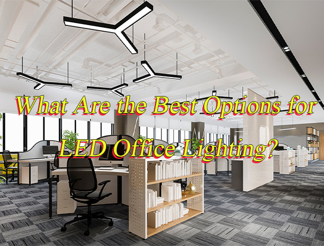
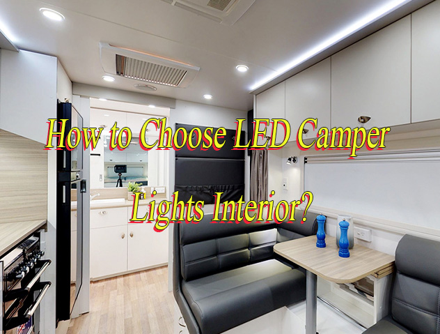
How to choose LED camper lights interior? Let’s discover selection guide, technical parameter, install methods, cost and lifespan for LED camper lights interior.
Are you worried about these problems?
- Does frequent vibration in camper cause LED lights to have loose connections and flicker?
- Are long lead times and high costs due to diverse vehicle models and lamp sizes an issue?
- Is balancing high brightness, low power consumption, and moisture resistance challenging?
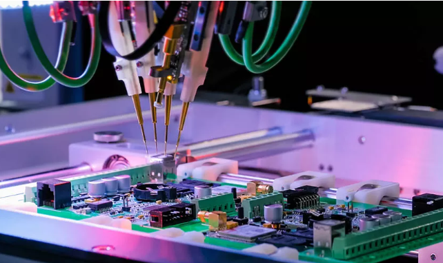
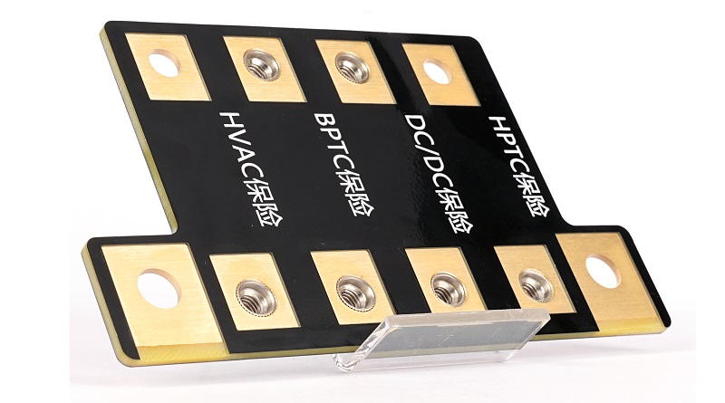
As a LED camper interior lights assembly service supplier, EBest Circuit (Best Technology) can provide you service and solution:
- Anti-vibration design: Serpentine routing + vibration-resistant pads ensure 200,000+ vibrations without loose connections, tripling lifespan.
- Modular rapid production: Supports 1-3m multi-size lamp belts, 72h prototyping, 3-day mass production, one-stop fit for all vehicle models.
- Power-heat balance: Layered heat dissipation + intelligent constant-current drive achieves high brightness without overheating, low power without dimming, reducing costs by 15%.
Welcome to contact us if you have any request for LED camper lights interior assembly: sales@bestpcbs.com.
How to Choose LED Camper Lights Interior?
Below is a guide to how to choose LED camper lights interior:
1. Accurate Calculation of Brightness Requirements
- Small sleeping area (≤4㎡): Requires soft lighting; recommended 100-150 lumens (approx. 1.5-2W LED lamp) to avoid strong light disrupting sleep.
- Kitchen/workbench (4-6㎡): Requires high-brightness task lighting; recommended 400-600 lumens (approx. 5-7W) for safe and clear operations like cutting or reading.
- Large activity area (≥6㎡): Recommended 800-1200 lumens (approx. 10-15W) for main lighting, paired with supplementary light strips (100-200 lumens/meter) for layered illumination.
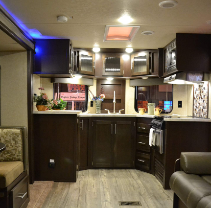
2. Color Temperature Selection and Scene Adaptation
- 2700K-3000K (warm white): Suitable for relaxation areas and bedrooms; creates cozy ambiance, mimics dusk natural light, and promotes melatonin secretion.
- 4000K-4300K (neutral white): Ideal for kitchens/bathrooms; balances brightness and comfort while minimizing shadow interference.
- 5000K-6000K (cool white): Recommended only for workstations/reading corners; enhances alertness but avoid prolonged use to prevent eye fatigue.
- Recommend dimmable fixtures (e.g., 2700K-6000K stepless adjustment) for multi-scene adaptability.
3. Dimming Function and Circuit Compatibility
- Essential PWM dimming: Supports 10%-100% stepless adjustment or three-level dimming (30%/70%/100%); nighttime use can reduce to minimum brightness to avoid glare.
- Voltage matching: Confirm vehicle DC system (12V/24V) and select corresponding LED voltage (tolerance ±10%) to avoid energy loss from added resistors.
- Dimmer compatibility: Use trailing-edge dimming technology for LED drivers to prevent flickering.
4. Energy Efficiency and Power Management
- Power control: Single-lamp power ≤10W; total multi-lamp system power ≤20% of battery capacity (e.g., 100Ah battery limited to 200W).
- Low standby power: Select fixtures with standby power <0.5W to prevent battery drain during long-term parking. Integrated drivers: Prefer LEDs with built-in constant-current drivers to eliminate flicker from voltage fluctuations, extending lifespan by >30%.
5. Protection Level and Structural Design
- Basic protection: Indoor fixtures require at least IP44 (splash-proof); kitchens/bathrooms recommend IP65 (dust-proof/waterproof).
- Material selection: Optimize for flame-retardant PC or aluminum housing with ≥1mm heat sink thickness to maintain operating temperature <60°C.
- Vibration resistance: Choose fixtures with silicone shock pads to withstand driving vibrations and prevent solder joint cracking.
6. Installation Methods and Wiring Optimization
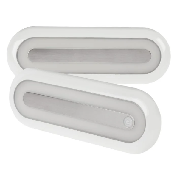
- Magnetic light strips: Suitable for temporary setups; magnetic force ≥2N/cm² (e.g., OPPKEPT series) for reusable adhesion without residue.
- Recessed spotlights: Precise hole matching required (common φ40mm/φ55mm); depth ≥20mm for heat dissipation space.
- Quick connectors: Prioritize XT30 or Anderson interfaces for tool-free plug-and-play, simplifying wiring complexity.
7. Additional Features Based on Demand
- Smart control: Bluetooth/WIFI-enabled fixtures support APP scene presets but require signal stability checks in remote areas.
- Power-off memory: Automatically restores dimming settings after restart to avoid reconfiguration.
- UV sterilization: Bathrooms may use 395nm UV-LED fixtures with independent switches and warning labels.
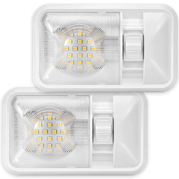
LED Interior Camper Lights Technical Parameter
| Parameter | Specification |
| Voltage Compatibility | 12V DC power as primary, some support 90-240V wide voltage input, needs to match vehicle power system |
| Power & Brightness | Reading lights: 3-5W (~300 Lumens); Main lights: 15-30W (up to 1000+ Lumens); High-efficiency LEDs: 90-120 Lumens/W |
| Color Temperature Selection | Warm white (2700-3500K for rest/reading areas), neutral white (3500-5000K for kitchen/work areas), cool white (5000-6500K for bathroom/storage areas) |
| Color Rendering Index (CRI) | ≥80 (basic requirement), high-quality products ≥90 (true color reproduction) |
| Waterproof Rating | Internal lighting: IPX-4 (splash-proof); Outdoor/humid environments: IPX-5 or higher recommended |
| Smart Dimming | Stepless brightness adjustment (knob/APP), some models support color temperature tuning or 16 million colors |
| Motion Sensing | Human motion detection for “turn on when detected, off when undetectable”; infrared/microwave sensors enhance sensitivity |
| Remote Control | Smartphone APP/remote control for on/off, timing, scene mode switching (e.g., reading mode, night light mode) |
| Interface Adaptability | G13 (fluorescent tube), E26/E27 (screw socket), magnetic/snap-fit designs; some support solar charging |
| Size Matching | Lamp dimensions must fit original vehicle space (e.g., 0.3m LED tube, 1.2m tri-proof light); adjustable brackets/hooks enhance flexibility |
| Safety Certification | Meets ECE-R128 automotive LED standards; passes CE, ROHS, PSE safety certifications |
| Protective Design | Insulated housing + electric shock protection + overvoltage/overcurrent protection; low UV radiation design |
How to Install LED Interior Camper Lights?
Below is a guide about how to install LED interior camper lights:
1. Planning and Design Enhancement
- Precise Positioning and Measurement: Use a laser distance meter to determine installation locations (e.g., ceiling beam gaps, 30cm below cabinets). Draft a 1:10 scale installation diagram. When calculating strip length, reserve 5% margin for cutting errors. Recommend 3528/5050 LED strip models with ≤2cm LED spacing for uniform illumination.
- Voltage Compatibility and Selection: Prioritize 12V DC low-voltage systems matching RV 12V/24V power systems. Recommended brands include Acegoo and Vansky dimmable models, supporting 0-100% brightness adjustment with measured range ≥300lm-1500lm for dual-purpose reading/ambient lighting.
- Waterproof Rating Selection: IP65 strips mandatory for high-traffic areas (e.g., kitchen countertops). For humid environments (e.g., bathrooms), IP67+ fully sealed fixtures recommended.
2. Comprehensive Tool and Material Checklist
Professional Tools:
- Insulated screwdriver set (PH2 crosshead/SL6 flathead), digital multimeter (e.g., Fluke 17B+), automatic wire stripper (0.5-6mm²), 2¼-inch Forstner bit (with impact drill).
- Specialty Tools: Heat gun (for waterproof terminal shrinkage), crimping tool (hexagonal crimping sleeves), laser level (for horizontal installation alignment).
Core Material Specifications:
- LED Strips: CE/ROHS certified, ≤0.5W per LED, total power ≤5W per meter.
- Cabling: 0.75mm² twisted-pair shielded wire (anti-interference), IP68-certified waterproof screw terminals.
- Protection Devices: 5A self-resetting fuses per circuit (response time <0.1s), recommended Littlefuse PTC models.
3. Enhanced Safety Operation Protocols
- Power-Off Verification: After shutting off main power, measure battery terminal voltage with multimeter DC voltage mode (should be ≤0.1V). Critical nodes include inverter outputs and solar charge controllers.
- Anti-Short-Circuit Measures: Insulate all exposed wire ends with electrical tape + heat-shrink tubing double protection. For recessed fixtures, maintain ≥2cm thermal dissipation clearance filled with thermal silicone.
4. Installation and Fixing Technical Details
Strip Installation:
- Surface Preparation: Clean installation surface with isopropanol, dry completely before applying 3M VHB double-sided tape (-40℃~150℃ resistant).
- Fixing Techniques: Reinforce every 30cm with stainless steel clips. For corners, use 45° miter cuts to avoid 90° bending causing light decay.
Recessed Fixture Installation:
- Drilling Alignment: Mark drill points with laser level, use Forstner bit perpendicular to wall.
- Sealing Treatment: Post-installation fill with silicone sealant (e.g., Dow Corning 795), ensure wiring ports face downward for drainage slope.
5. Standardized Wiring and Connection Procedures
- Polarity Identification: Use red/black dual-color wiring with red heat-shrink tubing marking positive terminal. Connections require dual-process soldering + waterproof terminals, with smooth conical solder joints (no cold solder/splashes).
- Parallel Circuit Design: Per-circuit total power ≤60W (matching 5A fuse). For multi-circuit parallel connections, adopt bus-type wiring (main bus ≥1.5mm²) to avoid voltage drop from long branch lines.
- Dimming System Integration: Dimming switches must match LED driver (e.g., PWM dimmers). Verify smooth dimming curve without flicker (frequency ≥200Hz).
6. Full Power-On Testing Protocol
- Segmented Testing: Start with single-circuit functional checks, gradually increase to full load. Monitor surface temperature with infrared thermography (normal operating temperature ≤60°C).
- Voltage Stability Verification: Use digital storage oscilloscope to monitor voltage waveforms. 12V systems allow ±3V fluctuation (11-14V); out-of-range requires power management system checks.
- Waterproof Performance Test: Conduct 24-hour post-installation spray test (3 bar pressure, 10 minutes), focusing on terminal seals and fixture gaskets.
7. Final Calibration and Long-Term Maintenance
- Optical Adjustment: Use adjustable angle brackets to direct light, avoiding direct eye exposure. Measure illuminance with light meter (≥300lux recommended for kitchen countertops).
- Maintenance Schedule: Quarterly terminal tightness checks, semi-annual surface cleaning (microfiber cloth + distilled water). Humid environments require additional quarterly seal inspections.
How to Replace Old LED Lights of Camper Interior?
1. Safety Disconnection and Tool Preparation
- Turn off the vehicle’s main power and the circuit switch for the corresponding area; remove the car key or disconnect the negative terminal of the battery to avoid electric shock risks.
- Prepare tools: insulated screwdriver, plastic pry bar, multimeter (optional), and new LED bulbs (must match the original model size and voltage; recommend choosing dedicated models with built-in decoding function).
2. Remove Old Lampshades and Bulbs
- Ceiling Interior Light: Open the glasses box, press the edge gap of the lamp body, and gently pry to remove the cover; observe internal clips or rotating structures, rotate the lampshade counterclockwise or release the clips, then pull out the old bulb.
- Trunk Light: Insert the plastic pry bar into the edge gap of the lamp body, gently pry to remove the lampshade; press the connector clip to unplug the power cord, release both clips, and take out the old bulb.
- Reading Light/Other Positions: Use a flat-head screwdriver to gently pry or rotate to disassemble according to the vehicle model; avoid excessive force to prevent damaging the lampshade.
3. Install New LED Bulbs
- Confirm the positive and negative poles of the new bulb (usually marked with “+”/”-” or determined by trial lighting), insert vertically into the socket interface, rotate clockwise or press the clip to fix.
- Reconnect the power cord, ensure the connector clip is tightly fastened to avoid poor contact; if soldering is required, use a soldering iron to heat the old solder joint, remove the old lamp beads, and solder the new lamp beads according to the original circuit.
4. Testing and Debugging
- Temporarily connect the power, turn on the lighting in the corresponding area, check if the new light is on, the brightness is uniform, and the angle is appropriate. If it does not light up, check the positive and negative poles or the connector connection; if the light angle is offset, adjust the bulb position or the lamp screws.
5. Restore and Clean
- Reinstall the lampshade, ensure the clips or rotating structures are firmly fixed; clean up dust or debris generated during the disassembly process.
- Turn on the full vehicle power for a final check, confirm all lighting functions are normal, and complete the operation.
How Long Does Camper LED Interior Lights Last?
Camper interior LED lights typically boast 50,000 to 100,000 hours of lifespan, equivalent to 15–30 years of regular use and far exceeding halogen bulbs. This exceptional durability stems from efficient heat dissipation (via aluminum bases) and low-energy operation. While actual longevity depends on usage patterns, voltage stability, and heat management, high-quality LEDs rarely “burn out” suddenly. Instead, they gradually dim over time (luminous decay). For campers, this translates to decades of maintenance-free, energy-efficient lighting with minimal battery drain.
How Much Does LED Camper Lights Interior Cost?
The price of LED interior lights for campervans in the European and American markets varies significantly depending on features, specifications, and brand: basic single lamps range from $7-$20, while smart dimming/color temperature models range from $25-$60.
By further breaking down the features, basic switch models range from $8-$15, three-level dimming with memory models from $22-$35, and app-controlled models with RGB color change from $40-$60. Small lamps (2-3 inches) cost $7-$12, while large panel lights (6-8 inches) cost $30-$50. Cost-effective brands (such as MICTUNING) range from $10-$25, while RV-specific brands (such as Lumitec) cost $30-$60 (IP67 waterproof and aircraft-grade aluminum).
The total cost of a complete vehicle interior upgrade is approximately $150-$500. For example, six basic lamps plus wiring/switches start at around $100, while smart solutions cost around $170 or more. Based on a 50,000-hour lifespan, the average daily cost is less than $0.01, saving 80% energy compared to halogen lamps and eliminating the need for frequent replacements (labor costs of $50 or more per replacement). When purchasing, it is recommended to give priority to mid-range models with aluminum heat dissipation + PC lens priced at $15-$25, and avoid choosing low-quality lights below $5 (which are prone to flickering and have poor heat dissipation).
Where Can I Buy Cost-Effective LED Camper Lights Interior?
Alibaba International
- Features: Global leading B2B platform for enterprise procurement, offering end-to-end foreign trade services for LED lighting.
- Strengths: AI-powered product selection tools, multilingual optimization, and regulatory compliance support (e.g., EU CE certification). 2025 European orders grew 45% YoY, with premium smart lighting in high demand in France/Italy. Pricing is 30-50% below Western markets, with profit margins up to 5-10x in Russia.
- Product Focus: 12V camper LED ceiling lights, dimmable reading lamps, motion-activated cabinet lighting.
- Note: Requires factory certifications and product compliance documentation; platform provides “Europe Billion Subsidy” traffic incentives.
eBay Motors
- Features: Specialized automotive/RV parts platform with integrated Fitment compatibility system.
- Strengths: myFitment tools enable precise vehicle matching, reducing return rates; cross-border sellers benefit from compatibility data optimization for search efficiency. Top-selling items include 12V multicolor LED ceiling fixtures and IP65-rated reading lights.
- Suitability: Ideal for SMEs and individual sellers for bulk/retail procurement.
Amazon
- Features: World’s largest retail e-commerce platform with extensive camper accessories category.
- Strengths: “Fast Shipping” badges and Prime delivery network; third-party tools (e.g., VioFitment) support ACES data upload for vehicle-specific matching. Best-sellers include high-efficiency reading lights and touch-sensitive dimmable ceiling fixtures.
- Regulatory Compliance: Mandatory adherence to regional safety standards (e.g., EU CE, U.S. UL certification).
Global Sources
- Features: Professional B2B platform specializing in international trade solutions.
- Value Proposition: One-stop procurement services including price benchmarking, real-time communication, and market intelligence. Covers full-spectrum automotive parts from engine components to electronic controls. 2025 Middle Eastern markets (Saudi Arabia/UAE) reported 30%+ growth in customized lighting demand.
- Product Highlights: Camper aluminum alloy ceiling lights, long-bar LED night reading lamps.
U.S. Retail Giants (Home Depot/Lowe’s/Wayfair)
- Features: Leading North American home improvement chains with O2O integration.
- Differentiators: Home Depot’s 2,200+ stores offer professional installation services; Lowe’s provides customizable lighting solutions; Wayfair targets cost-conscious female consumers with competitive pricing.
- Entry Requirements: Official channel partnerships (e.g., WAYLI Cross-Border Group) required for platform access, with stringent quality control.
Specialized RV Platforms
- Features: Auto parts data platform focused on vehicle compatibility optimization.
- Technical Advantages: Multi-platform (Amazon/eBay/Walmart) data synchronization with 1-3 week compatibility activation; bulk SKU management reduces operational costs; tailored for traditional export enterprises and cross-border transitioning factories.
- Use Case: Critical for sellers requiring precise camper vehicle data matching to enhance search visibility and conversion.
Southeast Asian/Emerging Market Channels
- Features: Platforms like Made-in-China and 1688 offer cost-competitive camper LED lighting.
- Growth Drivers: Vietnam/Southeast Asia smart LED market expanding >30% annually; supports small-batch customization (e.g., 12V square wall cabinet lights, touch-dimmable reading fixtures).
Welcome to contact us if you have any request for