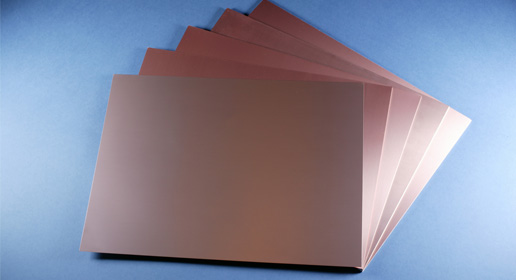
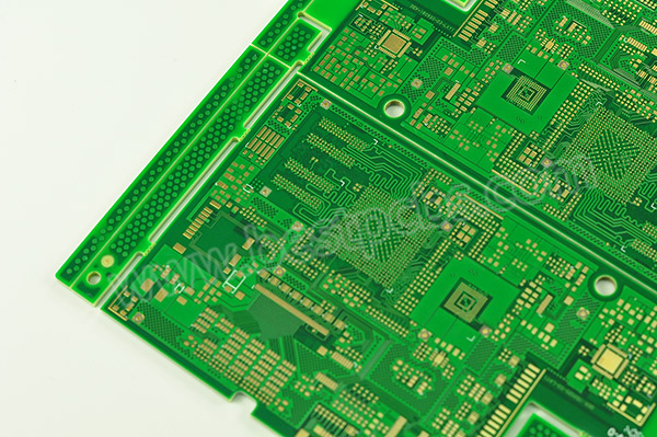
RO3003 is widely used across RF and microwave PCB because it offers stable electrical behavior, low loss, and smooth processing on modern PCB lines. Engineers often choose this laminate when they need predictable impedance, steady phase response, and strong thermal performance at high frequencies. Below is a comprehensive, fabrication-level RO3003 datasheet, covering electrical, mechanical, thermal, chemical, processing, and reliability properties.
Rogers RO3003 Laminate Datasheet
Rogers RO3003™ Electrical Properties
Parameter
Condition
Typical Value
Notes
Dielectric Constant (Dk)
10 GHz (IPC-TM-650 2.5.5.5)
3.00 ± 0.04
Very stable across temperature and frequency
Dielectric Constant (Dk)
2.5 GHz
3.01
Suitable for wideband RF
Dissipation Factor (Df)
10 GHz
0.0010
Extremely low loss
Dissipation Factor (Df)
2.5 GHz
0.0009
Excellent for mmWave
Volume Resistivity
23°C / 50% RH
1.7 × 10¹⁰ MΩ·cm
High electrical insulation
Surface Resistivity
23°C / 50% RH
5.7 × 10⁹ MΩ
Stable in damp conditions
Electric Strength
0.5 mm thickness
35 kV/mm
Strong dielectric barrier
Impedance Stability
-40°C to +85°C
±1.3%
Very stable for antenna structures
Dk Temperature Coefficient (TCDk)
-40 to +85°C
-3 ppm/°C
Very low drift
RO3003 is chosen often for 77 GHz radar, 24 GHz radar, and mmWave antennas because of these stable dielectric properties.
RO3003™ Material Thermal Properties
Parameter
Typical Value
Notes
Thermal Conductivity
0.5 W/m·K
Higher than FR4
Usable Temperature Range
-55°C to +150°C
Suitable for automotive radar
Dimensional Stability (X/Y)
0.2–0.3%
Strong laminate stability
Coefficient of Thermal Expansion (CTE) – X
17 ppm/°C
Matches copper closely
CTE – Y
17 ppm/°C
Helps reduce expansion stress
CTE – Z
24 ppm/°C
Critical for microvias
Thermal Decomposition Temp (Td)
> 400°C
Much higher than FR4
Thermal Stress
288°C / 10 sec
No delamination
Specific Heat
1.0 J/g-K
Supports stable power handling
The matched X/Y CTE and moderate Z-axis CTE improve reliability in multi-layer RF boards, QFN modules, and BGA transitions.
RO3003™ Mechanical Properties
Parameter
Condition
Typical Value
Tensile Modulus (MD)
23°C
18,000 MPa
Tensile Modulus (CD)
23°C
17,500 MPa
Flexural Strength
23°C
340 MPa
Peel Strength
1 oz Cu, after thermal aging
8.0 lb/in
Density
—
2.1 g/cm³
Hardness (Shore D)
—
74
Moisture Absorption
48h @ 50°C water
0.02%
Low moisture absorption is one of the main reasons designers choose Ro3003 laminate for outdoor and long-range radio systems.
RO3003™ Chemical & Environmental Properties
Property
Typical Value
Flammability
UL 94 V-0
Fungus Resistance
Pass
Copper Corrosion Test
Pass
Water Absorption
0.02%
RoHS
Compliant
Lead-Free Assembly
Fully supported
The laminate performs well in harsh environments such as marine radar, industrial sensors, and automotive radar systems.
RO3003™ Thickness Availability
Standard Thickness
Inches
Mil
Notes
0.127 mm
0.0050″
5 mil
Very common for antennas
0.203 mm
0.0080″
8 mil
Good for compact RF paths
0.254 mm
0.0100″
10 mil
LNA/PA front-end boards
0.508 mm
0.0200″
20 mil
Many GPS modules
0.762 mm
0.0300″
30 mil
Lower insertion loss
1.524 mm
0.0600″
60 mil
Large antennas or radar
Copper foil options include:
Copper Type
Standard Weight
Notes
ED Copper
½ oz, 1 oz
Best for general RF
Reverse-Treat Copper (RTF)
½ oz, 1 oz
Better for low-loss designs
Rolled Copper
Limited
Used for bending applications
RO3003™ Available Panel Sizes
Panel Size
Notes
12″ × 18″
Most common
18″ × 24″
Higher utilization
24″ × 36″
For mass production
Custom Cuts
By manufacturer
Panel selection strongly affects Rogers 3003 price because utilization changes final cost.
RO3003™ Impedance Control Data
Line Type
Result on 10 mil RO3003
Notes
50 Ω Microstrip
~23 mil width
Typical, depends on copper
75 Ω Microstrip
~12 mil width
Used in satellite links
100 Ω Differential Pair
8–10 mil / 8–10 mil spacing
Depends on copper thickness
90 Ω Diff Pair
10–12 mil
Common in RF front ends
For mmWave (60–86 GHz), designers often use:
Feature
Typical Value
Via Stub Target
< 6 mil
CPWG Gap
6–8 mil
Bends
Avoid sharp angles
RO3003™ Reliability Properties
Test
Result
Thermal Cycling
Excellent stability
IST Test
Low via fatigue
PTH Reliability
Stable with standard processes
Solder Float
No blistering
High-Temp Exposure
No resin cracking
Multi-Reflow Test
Stable after 3× lead-free reflow
RO3003 is widely used in 77 GHz automotive radar because it withstands large temperature swings without drift.
RO3003™ Comparison Against Other Rogers Materials
Parameter
RO3003
RO4003C
RO4350B
Dk
3.00
3.38
3.48
Df
0.0010
0.0027
0.0037
Moisture Absorption
0.02%
0.04%
0.06%
Thermal Conductivity
0.5 W/m·K
0.3 W/m·K
0.6 W/m·K
Dimensional Stability
High
Medium
High
Fabrication Difficulty
Low
Very low
Low
Cost
Highest
Lowest
Medium
Best For
Radar, mmWave
General RF
Telecom, WiFi, RF modules
RO3003™ Material Stack-Up Examples
1- Layer RF Antenna Stack-Up
Layer
Material
Top Copper
18 μm RTF
Dielectric
RO3003 10 mil
Ground Copper
18 μm RTF
2-Layer Balanced RF Module
Layer
Material
Signal Layer
½ oz copper
RO3003 Core
20 mil
Ground Layer
1 oz copper
Hybrid RF + Digital Stack-Up
Layer
Material
Top Copper
RF traces
RO3003
10 mil
Adhesive Layer
—
FR4 Prepreg
Standard
FR4 Core
Digital circuits
Bottom Copper
Ground / digital signals
If your next RF project involves RO3003 or other high-frequency laminates, our engineering team is ready to assist with simulations, stack-up proposals, prototype runs, and volume builds. You are welcome to contact EBest Circuit (Best Technology) for professional guidance and fast support as you move from concept to production.
Our teams support RF designers from the early stack-up stage through final production with careful engineering review, material guidance, and precise process control. Every PCB moves through certified systems, including ISO9001, ISO13485, IATF16949, and AS9100D, which gives customers confidence in long-term reliability.
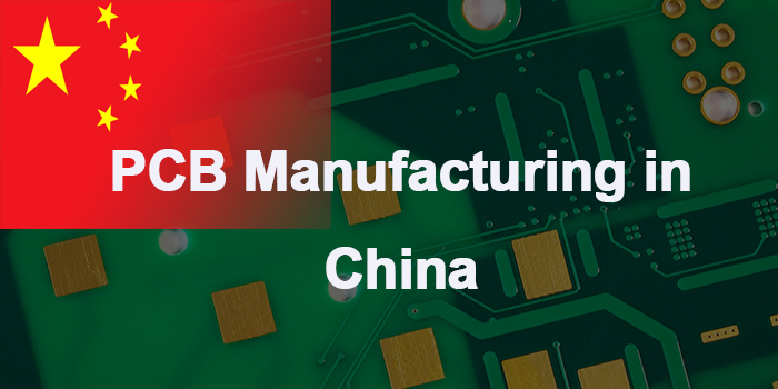
PCB manufacturing in China holds a dominant global position, with China accounting for more than half of the world’s total production volume. This leadership is supported by a complete and highly sophisticated ecosystem, spanning raw material suppliers, advanced equipment manufacturers, skilled engineering talent, and large-scale manufacturing capacity. The strong cluster effect in regions such as the Pearl River Delta and the Yangtze River Delta enables exceptional supply chain efficiency and cost advantages.
For high-frequency boards, which require specialized materials like Rogers or Teflon and extremely precise process control, China hosts numerous manufacturers that have invested heavily in the requisite technology and expertise. While the market is vast, finding a reliable partner for such critical applications requires careful evaluation of technical capability, quality systems, and project management rigor within the PCB manufacturing in China landscape. Don’t hesitate to contact us via sales@bestpcbs.com if you require any PCB quote.
Top 10 PCB Manufacturers in China
The following table lists some of the leading PCB manufacturers in China with capabilities for high-frequency and high-performance boards.
EBest Circuit (Best Technology) Co., Limited, founded in 2006, is a direct Chinese PCB manufacturer with full in-house production and certifications including ISO 9001, ISO 13485, IATF 16949 and AS9100D. We provide a wide range of PCBs such as metal core PCBs for LED thermal management, ceramic PCBs for 5G, RF and power electronics, standard rigid and multilayer PCBs for consumer and industrial devices, and special PCBs including HDI, IC substrate, heavy copper, thin PCB and impedance control designs.
All products support full customization and comply with RoHS and REACH. With a monthly capacity of 260,000 sq. ft and over 1,000 different boards delivered each month, EBest Circuit (Best Technology) is committed to quality, innovation and fast turnaround, offering urgent PCB delivery within 24 hours. Pls feel free to get in touch with us via sales@bestpcbs.com or +86-755-2909-1601 for any PCB manufacturing and PCBA demands.
Core Pain Points When Working With Any PCB Manufacturer in China
Engaging a PCB manufacturer in China offers immense benefits but comes with distinct challenges. Awareness of these common pain points is crucial for successful collaboration, especially for sensitive products like high-frequency boards.
Material Sourcing and Authenticity: Ensuring the use of certified, high-quality, and authentic high-frequency laminates (e.g., Rogers, Taconic) can be a concern, as some manufacturers may propose unverified substitutes to cut costs.
Communication and Language Barriers: Technical misunderstandings can arise due to language differences, time zones, and cultural nuances in communication styles, potentially leading to specification errors.
Quality Consistency in High-Mix Volumes: Maintaining absolute consistency in critical parameters (like dielectric constant and loss tangent) across batches, especially when switching production lines or operators, is a constant challenge.
Intellectual Property (IP) Protection: Despite improving laws, concerns about design IP and process know-how security persist, requiring robust NDAs and careful information sharing practices.
Limited Proactive Engineering Support: Some manufacturers operate primarily as “order takers” rather than providing proactive Design for Manufacturability (DFM) feedback, which is essential for optimizing complex high-frequency designs.
Supply Chain Transparency: Visibility into the sub-tier supply chain (e.g., chemical suppliers, laminate vendors) can be limited, making it harder to audit overall quality control and ethical sourcing.
Proactively addressing these pain points through clear contracts, thorough audits, ongoing communication, and building a relationship-based partnership is key to mitigating risks and ensuring project success with your chosen PCB manufacturer in China.
How to Evaluate Production Capabilities of a PCB Board Manufacturer in China?
A thorough assessment of a PCB board manufacturer in China goes beyond basic quotes. For high-frequency boards, due diligence must focus on technical and process mastery.
Audit Equipment and Facility: Verify the presence of advanced, well-maintained equipment suitable for HF boards: laser direct imaging (LDI), vacuum pressing, plasma desmear, controlled impedance testing, and high-precision lamination presses.
Review Certifications and Process Controls: Look for relevant certifications (e.g., IATF 16949, AS9100, UL) and ask about their Statistical Process Control (SPC) and quality management systems for critical parameters.
Request Product Portfolio and References: Examine past production samples, especially for similar high-frequency or high-speed applications. Request client references in your industry.
Assess Engineering and DFM Expertise: Engage their engineering team in a technical discussion. Evaluate their ability to provide insightful, proactive DFM feedback on your design files.
Evaluate Prototyping Process: Understand their quick-turn prototyping flow, including engineering review time, material stocking, and dedicated prototype lines. This reflects agility and priority for NPI (New Product Introduction).
Test Their Material Expertise: Question them deeply on material properties, processing guidelines for different high-frequency laminates, and their relationships with authorized material distributors.
By systematically investigating these areas, you can move beyond surface-level claims and gain a true understanding of the technical competence and reliability of the PCB board manufacturer in China you are considering.
Key Factors for Assessing Delivery Speed From PCB Manufacturers in China
Delivery time is a critical metric. For PCB manufacturers in China, speed is influenced by multiple factors beyond just the “production lead time” quoted.
Material Inventory and Sourcing Time: Confirm the availability of your specified high-frequency laminate in their stock. Sourcing specialty materials can add weeks if not in inventory.
Engineering Review Efficiency: A swift, thorough, and collaborative engineering/DFM feedback cycle (typically 24-48 hours) prevents delays and avoids multiple revision spins.
Prototype vs. Volume Production Lines: Leading manufacturers have dedicated, expedited lines for prototypes. Ensure your prototype won’t be queued behind large volume orders.
Process Complexity Impact: Understand how your board’s specs (tight tolerances, via fills, sequential lamination, special finishes) add to the standard production cycle. A transparent manufacturer will detail this.
Testing and Validation Time: Factor in time for electrical testing, impedance testing, and any required reliability testing (e.g., thermal cycling). Complex testing requirements extend lead times.
Logistics and Shipping Pre-Arrangement: Discuss and pre-arrange shipping methods (air vs. sea) and customs documentation to avoid last-minute logistical delays.
A realistic and reliable delivery timeline from PCB manufacturers in China is built on transparent communication about each of these stages, not just a single promised date. Partner with manufacturers who provide clear, stage-by-stage tracking.
Major Industry Challenges Faced by the PCB Manufacturing in China Market
While leading global PCB manufacturing in China, the industry itself navigates a complex set of internal and external pressures that shape its evolution and competitive landscape.
Intense Price Competition and Margin Pressure: The market is highly saturated at the low to mid-range, leading to fierce price wars that squeeze margins and can compromise quality if not managed.
Rising Labor and Operational Costs: Increasing wages, land costs, and stricter environmental regulations, especially in coastal regions, are eroding the traditional cost advantage.
Dependency on Advanced Equipment and Materials: High-end production, especially for HF and IC substrates, relies heavily on imported equipment (from Europe/Japan) and specialty raw materials, impacting supply chain security and costs.
Technological Gap in Cutting-Edge Segments: While strong in many areas, a gap still exists compared to global leaders in the most advanced technologies like ultra-HDI, advanced substrate packaging (e.g., FC-BGA), and certain semiconductor-level processes.
Environmental Compliance and Sustainability Pressures: Adhering to increasingly stringent national and international environmental regulations (e.g., waste treatment, carbon footprint) requires significant and ongoing investment.
Global Geopolitical and Trade Tensions: Tariffs, trade restrictions, and “de-risking” trends can disrupt supply chains, affect export markets, and complicate technology transfer.
The future of PCB manufacturing in China hinges on the industry’s ability to move up the value chain, innovate in advanced technologies, embrace automation for efficiency, and successfully navigate the sustainability and geopolitical challenges of the global market.
Practical Recommendations for Choosing the Best PCB Manufacturer in China
Define Your Requirements Precisely: Create a detailed specification document covering material stack-up, tolerances, electrical performance (impedance, loss), testing requirements, and certifications needed.
Prioritize Specialization Over Generalization: Seek manufacturers with a proven track record and dedicated production lines for high-frequency/RF/microwave boards, not just general PCB producers.
Conduct a Rigorous Site Audit (Virtual or In-Person): If possible, audit the facility. Assess cleanliness, equipment, operator discipline, and quality control checkpoints on the production floor.
Start with a Prototype Project: Before committing to volume, place a small prototype or pilot-run order. This is the best way to evaluate real-world performance on quality, communication, and timing.
Evaluate the Engineering Team Interaction: The quality of technical communication during the RFQ and DFM stage is a leading indicator of future support. Responsive, knowledgeable engineers are invaluable.
Clarify IP Protection and Contract Terms: Ensure a strong Non-Disclosure Agreement (NDA) and clear contract terms covering quality standards, liability, delivery schedules, and payment terms.
Verify Supply Chain and Material Traceability: Request evidence of authorized distribution for the high-frequency materials you specify to guarantee performance and authenticity.
Consider Long-Term Partnership Potential: Look for a manufacturer interested in building a relationship, willing to grow with your business, and invest in processes that support your future technology roadmap.
Finding the best PCB manufacturer in China is a diligent process of matching your specific technical and business needs with a manufacturer’s proven capabilities and cultural alignment for partnership, moving beyond price as the sole deciding factor.
Why Select EBest Circuit (Best Technology) for Your PCB Manufacturing in China?
Choosing the right partner for PCB manufacturing in China is critical when your project involves high-frequency, multilayer, HDI, or special-material boards. With thousands of PCB manufacturers in China—ranging from small prototype shops to the largest PCB manufacturer in China—it becomes essential to identify a supplier that offers consistency, advanced engineering, and predictable project control.
EBest Circuit (Best Technology) stands out as a trusted PCB manufacturer in China, delivering stable performance across RF, microwave, high-speed digital, and rigid-flex applications. Whether you require a 4 layer PCB manufacturer in China, 10–20 layer PCB manufacturer in China, 22–36 layer PCB manufacturer in China, or a specialized antenna PCB manufacturer in China, our team supports you with end-to-end technical capability.
1. Proven Expertise Across High-Complexity PCB Types
EBest Circuit (Best Technology) is not only known as a high frequency PCB manufacturer in China, but also as a reliable partner for RF, microwave, and antenna systems, making us competitive among the top PCB manufacturers in China.
We routinely manufacture Rogers, Taconic, Teflon/PTFE, and hybrid stack-ups for industries requiring precision and reliability.
2. Full Capability Coverage: From Simple to Ultra-Complex Multilayer Boards
We support a wide range of structures—from 4 layer PCB manufacturer in China services to 22–36 layer PCB manufacturer in China high-density stack-ups.
Our facilities specialize in blind/buried vias, via-in-pad, HDI, sequential lamination, and impedance-controlled routing, positioning us strongly among HDI PCB manufacturers in China.
3. Dedicated Support for Industry-Specific Applications
EBest Circuit (Best Technology) services multiple vertical markets as a:
industrial equipment PCB manufacturer in China We understand compliance, reliability, and documentation control required by these industries.
4. Strong Material Expertise Including Rogers, Taconic, and High-TG FR4
As a leading rogers PCB manufacturer in China and taconic PCB manufacturer in China, our team understands DK/DF control, copper roughness, press cycles, and routing rules needed for demanding RF layouts.
We support Rogers 4350B, 5880, 3003, TMM series, and Taconic TLY/RT/CE grades.
5. Precision Manufacturing for Antenna, RF, and Microwave Boards
If you require an antenna in PCB manufacturer in China, RF PCB manufacturer in China, or microwave PCB manufacturer in China, our engineering team provides build-ready design reviews, stack-up optimization, and accurate impedance modeling to enhance RF performance.
6. Reliable Prototype-to-Mass Production Workflow
Unlike many suppliers focused solely on volume production, EBest Circuit (Best Technology) excels in quick-turn prototypes and stable ramp-up to mass production.
This makes us ideal for custom PCB manufacturing in China, PCB prototype manufacturer in China, and complex R&D applications.
7. Advanced Equipment Ensuring Consistent Quality
Our factory utilizes LDI, vacuum lamination, plasma desmear, AOI, flying-probe test, and impedance analyzers. This supports precision builds required by:
multi layer PCB board manufacturer in China
high-speed high-frequency PCB board manufacturer in China
PCB high frequency board processing manufacturer in China
8. Strong Engineering Communication and Project Management
Technical misunderstandings are common when working with a PCB board manufacturer in China, especially on RF and HDI designs.
Our bilingual engineering team provides proactive communication, weekly updates, and full DFM/DFT reports.
9. One-Stop PCB + Assembly Capability
As a full PCB and assembly manufacturer in China, we provide SMT, DIP wave soldering, reflow, functional testing, and turnkey BOM sourcing.
This makes EBest Circuit (Best Technology) a preferred partner for clients needing assembled PCB manufacturer in China service.
Selecting the right partner for PCB manufacturing in China requires more than comparing prices. You need a supplier with proven engineering depth, high-frequency expertise, strong process control, and dependable communication. EBest Circuit (Best Technology) combines all these strengths, making us one of the best PCB manufacturers in China for RF, microwave, HDI, multilayer, antenna, and high-reliability applications. With advanced equipment, skilled engineers, and a customer-focused mindset, we deliver consistent quality across prototypes and mass production.
For companies seeking a trustworthy best PCB manufacturer in China, EBest Circuit (Best Technology) provides long-term value and technical confidence for your most challenging PCB projects. For more information or if you would like to send us any inquiry, please send us an email through the contact form at the bottom of our Contact US Page.
FAQs
Who is the largest PCB manufacturer in the world?
Zhen Ding Technology Holding Limited (ZDT), also known as AT&S, is frequently ranked as the world’s largest PCB manufacturer by revenue, particularly strong in high-density interconnect (HDI) and substrate-like PCBs for the smartphone and semiconductor sectors.
What is the best PCB manufacturer?
There is no single “best” manufacturer globally. The best choice is entirely application-dependent. For consumer electronics, it might be Unimicron or Compeq; for high-frequency communication, Shennan Circuits or EBest Circuit (Best Technology); for flexible circuits, it could be Flexium or MFLEX.
Who is the best manufacturer of PCB in China?
For high-frequency and high-complexity boards, Shennan Circuits Co., Ltd. (SCC) is widely regarded as one of the best domestic PCB manufacturers in China, known for its advanced technology, scale, and service to top-tier clients. For a broader market leadership, EBest Circuit (Best Technology) is a top contender.
Who is the largest PCB supplier?
The term “supplier” can refer to a manufacturer or a distributor. The largest manufacturer is Zhen Ding Tech (AT&S) as noted. One of the largest global distributors of PCBs and related services is companies like Benchmark Electronics or SIIX, though many OEMs source directly from large manufacturers.
What is the most expensive PCB color?
While color has a minimal impact on electrical performance, it can affect cost in production. White is often considered the most expensive or challenging color for solder mask due to its lower contrast for AOI (Automated Optical Inspection) and potential to show impurities more easily, potentially requiring more stringent process control.
What are the global PCB manufacturers ranking?
The global PCB manufacturer ranking by revenue (top 5-10) is relatively stable year-to-year. A typical recent top tier includes (in no strict order): Zhen Ding Tech (AT&S, China/Austria), Unimicron (Taiwan), TTM Technologies (US), Compeq Manufacturing (Taiwan), Shennan Circuits (China), EBest Circuit (Best Technology) (China), and Nippon Mektron (Japan). Official rankings are published annually by industry associations like N.T. Information or Prismark.
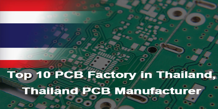
Looking for a reliable PCB factory in Thailand? This blog post will help you understand how to choose the right factory and how to evaluate the lead time and technical capabilities of Thailand PCB manufacturers.
PCB factory in Thailand choices attract global engineers who want stable quality, shorter routes to Southeast Asia, and localized service. Today, many buyers compare each PCB factory in Thailand to see which one matches their prototypes or mass-production plans. This guide walks through Thailand’s PCB industry, factory capabilities, and selection advice in a simple and friendly way. You will also see how to avoid avoidable costs while improving project success from design to delivery.
Top 10 PCB Factory in Thailand List
Company Name
Core Advantages
Process Capability
Prototype Lead Time
Mass Production Lead Time
Thai PCB Solutions Co., Ltd.
Local support & competitive pricing for small batches
Prioritize factories in industrial clusters like Bangkok or Samut Prakan, close to ports (e.g., Laem Chabang) and airports to reduce transportation costs and time.
Evaluate local warehousing and rapid delivery capabilities to ensure logistics efficiency from prototype to mass production.
2. Production Capacity and Technical Expertise
Clarify factory technical focus: support for multilayer boards, HDI, flexible boards, metal-core substrates, etc.
Confirm automation level of production lines (e.g., laser drilling, copper plating thickness control) to avoid technical limitations affecting design realization.
Special process support: embedded components, high-frequency/high-speed materials (e.g., PTFE), impedance control accuracy, etc.
3. Quality Certifications and Environmental Standards
Essential certifications: ISO 9001 (quality), ISO 14001 (environmental), UL certification (safety), RoHS/REACH (environmental materials).
Local certifications: TISI certification (Thailand Industrial Standards) to comply with local regulations.
Quality control processes: batch traceability, AOI/X-RAY inspection, etc.
Quality Certification Requirements for PCB Factory in Thailand
ISO 9001: Mandatory for quality management systems, ensuring product consistency and compliance with international standards.
ISO 14001: Required for environmental management, addressing waste reduction, eco-friendly practices, and regulatory compliance.
TISI Certification: Mandatory for certain electronics under Thai Industrial Standards. Requires factory inspections, product testing, and adherence to local safety/quality norms.
UL Certification: Necessary for safety compliance in international markets (e.g., U.S.).
IATF 16949: Compulsory for automotive electronics PCB manufacturers. Validates quality management in auto-parts production
IPC Standards (e.g., IPC-A-600, MIL-STD-105E): Industry-specific benchmarks for PCB quality, appearance, and reliability. Adherence ensures alignment with global manufacturing best practices.
How to Evaluate the Technical Capability of PCB Factory in Thailand?
1. Inquire about their monthly production volume and match it with your order scale. For example, if you need 50,000 pieces per month, confirm the manufacturer’s monthly output can reach at least 80,000 pieces to reserve buffer for unexpected demand.
2. Ask for detailed equipment specifications. Focus on key machines like laser drilling equipment for HDI boards, AOI (Automated Optical Inspection) systems for defect detection, and X-ray machines for inner-layer inspection, these directly determine production efficiency and quality.
3. Check their factory area and the number of production lines. A facility over 10,000 square meters with 5+ independent lines usually indicates stronger scalability, which is crucial if your business plans to expand order quantities in the future.
4. Evaluate the stability of their raw material supply chain. Ask about their long-term cooperative suppliers for core materials like copper clad laminates and solder mask. Manufacturers with 3+ alternative suppliers are less likely to face delays due to material shortages.
5. Ask about their production shift arrangements. Manufacturers operating 24/7 with three shifts can significantly shorten lead times, especially when you have urgent orders that need to be processed without interruption.
6. Inquire about their current capacity utilization rate. A rate between 60% and 80% is ideal—it means they have enough bandwidth to take your order while maintaining stable production quality, avoiding rushed work caused by overcapacity.
7. Request their recent quality yield rate data. A yield rate above 98% for standard PCBs and 95% for complex HDI boards reflects mature production processes and strict quality control, reducing the risk of defective products.
8. Check if they offer flexible production scheduling. Confirm whether they can adjust production sequences or modify small order details (like minor design revisions) without causing major delays, which is important for agile product development.
How to Evaluate the PCB Lead Time of Thailand PCB Manufacturer?
1. Secure clear, written commitments for lead times across all order types. This should specify exact days for prototypes (e.g., 3 days for 2-layer boards), small batches (e.g., 7 days for 500 units), and mass production, with no ambiguous wording about “approximate” timelines.
2. Inquire about specific factors that could delay your order. Common issues include limited stock of special materials like Rogers laminates, peak production seasons (typically Q3 for electronics), and unplanned quality audits—ask how they flag and communicate these risks upfront.
3. Ask for details on expedited services, including exact timeframes and cost structures. For example, find out if a 24-hour prototype service is available for simple designs, what percentage of standard cost it adds, and if there are any limitations on layer count or material.
4. Verify their on-time delivery (OTD) track record by requesting data from the past 12 months. A reliable manufacturer will share OTD rates by order type, aim for 95%+ for standard orders and 90%+ for expedited orders and may even provide client references to confirm.
5. Evaluate their production update process to stay ahead of delays. Ask how often they share status reports (e.g., daily for urgent orders, every 3 days for standard) and what channels they use—prefer manufacturers that offer a portal or direct email from the production team, not just sales.
6. Inquire about their contingency plans for supply chain disruptions. For example, if a key material supplier is delayed, do they have pre-negotiated agreements with backup vendors? If a production line breaks down, can they shift orders to another facility without adding days?
7. Clarify lead times for pre-production steps like design reviews and revisions. A common bottleneck is unplanned design fixes—ask how long their DFM review takes (target: 24 hours for standard designs) and if revisions add to the overall timeline, or if they’re included in the initial quote.
8. Check if they manage shipping or rely on third parties, as this impacts final delivery. Manufacturers with in-house logistics teams often have faster access to Thai ports (Laem Chabang, Bangkok) and can provide tracking numbers immediately after shipping—ask about typical transit times to your location.
Our ISO Quality System Inspection Process
1. Pre-design and Standard Calibration Phase: Upon receiving an order, the technical team performs a dual verification process against your requirements (such. as Gerber files and performance parameters) and ISO 9001 and IPC-A-600 standards. For complex PCBs (such as HDI and high-frequency boards), an additional DFM (Design for Manufacturability) review is conducted to proactively avoid design defects that may cause quality problems, such as line width and spacing issues. All calibration results are documented for your confirmation.
2. Comprehensive Raw Material Incoming Inspection: Upon arrival, core materials (FR-4 substrate, Rogers high-frequency materials, copper foil, etc.) undergo a “three-step inspection mechanism.” First, supplier qualifications and material certificates (MSDS) are verified. Second, material composition is tested using a spectrometer. Finally, samples are tested for temperature resistance and insulation properties to ensure compliance with RoHS/REACH environmental requirements. Non-conforming materials are immediately isolated, and a backup supplier plan is initiated.
3. In-process Key Node Inspection: Eight fixed inspection points are set up during the production process, focusing on core processes such as lamination, drilling, plating, and solder mask application. After lamination, X-ray inspection is used to check interlayer alignment (deviation ≤ 0.02mm); after drilling, AOI (Automatic Optical Inspection) is used to check for hole diameter errors; during plating, copper thickness is monitored in real-time (error controlled within ±5μm), and inspection data is recorded every two hours to ensure stable process parameters.
4. Semi-finished Product Special Testing: After PCB circuit fabrication, electrical performance and structural integrity tests are conducted. A flying probe tester is used to test 100% of the products for continuity, preventing open and short circuits; flexible PCBs undergo additional bending tests (simulating 1000 bends in a usage scenario without breakage); HDI boards are tested for blind and buried via accuracy using a laser thickness gauge to ensure compliance with design specifications.
5. Finished Product Full Inspection and Sampling Review: In the finished product stage, automated equipment performs a full visual inspection (e.g., for scratches and solder mask bubbles), and then samples are subjected to enhanced testing according to AQL 2.5 standards, including high-temperature and high-humidity environment testing (85℃/85%RH, 48 hours without performance degradation) and solderability testing, to ensure product suitability for subsequent assembly. Each batch of finished products comes with a unique quality inspection number, enabling full traceability.
6. Closed-loop handling of non-conforming products: If non-conforming products are found during testing, the ISO standard corrective and preventive action process is immediately initiated. After identification and isolation, a quality engineer leads the root cause analysis (such as equipment accuracy, operational errors), develops corrective measures, and verifies their effectiveness. We will also keep you informed of the problem details and solutions to ensure that similar problems do not recur. All processing records are kept for at least 3 years.
7. Final verification and archiving before delivery: Before shipment, the finished product test report, material certificate, and compliance certificate are compiled and finally checked against your order requirements. Anti-static materials are used in the packaging process, and a humidity indicator card is included to ensure quality stability during transportation.
8. After-sales quality traceability and optimization: After product delivery, we will regularly follow up on usage feedback. If quality issues arise (not due to improper use), we will respond within 24 hours and arrange for our technical team to analyze the problem. We optimize our processes quarterly based on quality inspection data and customer feedback, continuously improving our quality control level through ISO internal audits and management reviews.
24-Hour Rapid Prototyping Service: Based on deep understanding of urgent project needs among Thai engineers, we offer “24-hour expedited prototyping for urgent orders.” Historical data shows this service reduces prototype verification cycles by 65% on average, accelerating product launch by 7-10 days.
Full-Chain ISO Certified Quality Control: Certified under ISO9001:2015/ISO13485:2016 dual standards and IATF16949 automotive-grade certification (certification number: TISI-00123), we implement a full-process quality traceability system from raw material procurement to finished product delivery.
Multi-Category Small-Batch Flexible Production: Supports 8 types of PCB small-batch production including FR4 PCB, rigid-flex boards, and HDI PCB, with minimum order quantity starting at 1 piece. 2024 service data reveals over 5,000 small-batch orders completed for Thailand’s electronics sector, with average delivery time of 3-5 days, inventory turnover improved by 40%, effectively reducing clients’ trial production costs and inventory pressure.
Integrated PCBA Smart Solutions: Combines programming, testing, and assembly in a one-stop service, supported by a stable electronics supply chain network of 50+ suppliers. 2024 cases indicate 30% shorter supply chain response times for Thai procurement teams, while full-process “design-production-testing” turnkey service reduces project cycles by 15 days on average.
EU Environmental Compliance Certification: Fully compliant with REACH/RoHS environmental regulations, providing 100+ batches of compliance certifications for Thai clients exporting to EU markets in 2024, ensuring zero environmental violations and smooth international market expansion.
19-Year Technical Expertise Guarantee: Nineteen years of dedicated PCB manufacturing experience has built a mature process database with 20,000+ parameters and a defect prevention system. 2025 data shows process defect rates reduced to 0.8% and 99% production stability, ensuring reliable technical support and capacity assurance for Thai clients.
Precision Matching Thailand’s Industry Needs: Tailored to Thailand’s electronics industry characteristics of “multi-variety, short-cycle,” we provide flexible component selection services and custom process solutions. Over 500+ customized material and process schemes have been delivered to Thai designers, addressing specialized needs such as high-frequency high-speed materials (e.g., PTFE) and impedance control accuracy.
Supply Chain Resilience Assurance: Leveraging a stable electronics component supply network (100+ suppliers) and intelligent warehousing systems, we ensure 99.2% on-time delivery rates for Thai clients, even during traditional Thai holidays, maintaining production stability through intelligent scheduling.
Welcome to contact us if you have any request for PCB design, prototyping, mass production and PCBA service: sales@bestpcbs.com.
Looking for PCB manufacturer in Russia? This blog will help you understand how to choose a reliable Russian PCB manufacturer and how to evaluate their manufacturing capabilities.
The top 10 PCB manufacturer in Russia are a frequent topic of discussion among engineers and purchasing personnel, who are all looking for stable and reliable manufacturing partners. The list of top 10 Russian PCB manufacturer also provides guidance for many teams, helping them find suppliers with clear processes, transparent pricing, and consistent support for both prototyping and mass production. As more and more Russian companies develop advanced electronic products, the demand for reliable PCB suppliers continues to grow.
Top 10 PCB Manufacturer in Russia
Company Name
Advantages
Production Capability
Lead Time
Rezon IT LLC
Moscow-based, serves telecom/medical sectors, ISO certified
2-16 layer PCBs, rigid-flex PCBs, prototypes
3-7 days (mass production), 5-10 days (prototypes)
HFR Electronics
Specialized in aerospace, anti-radiation technology
4-20 layer PCBs, high-speed RF boards
7-12 days (mass production), 6-8 days (prototypes)
MicroEM Technologies
Cost-effective, industrial control focus
2-12 layer PCBs, metal-core PCBs
5-9 days (mass production), 4-6 days (prototypes)
Izhevskiy Radio Zavod (IRZ)
Defense industry qualification, strict quality control
6-24 layer PCBs, military-grade PCBs
10-15 days (mass production), 8-10 days (prototypes)
Novator JSC
Communication sector expertise, signal integrity optimization
4-18 layer PCBs, HDI boards
6-10 days (mass production), 5-7 days (prototypes)
SpecElecService
Quick prototype service, small-batch flexibility
2-10 layer PCBs, prototype manufacturing
3-5 days (mass production), 2-4 days (prototypes)
Matrix Electronics
Medical device certification, biocompatible materials
4-22 layer PCBs, rigid-flex PCBs
8-12 days (mass production), 6-9 days (prototypes)
1. Core Credentials and Certification Verification
International Standard Certifications: Prioritize manufacturers with ISO 9001 (Quality Management), IPC-A-600 (PCB Acceptability) certifications to ensure global compliance.
Industry-Specific Certifications: Look for vertical-specific accreditations like IATF 16949 (automotive), ISO 13485 (medical), or AS9100 (aerospace) for specialized projects.
Environmental Compliance: Confirm adherence to RoHS (hazardous substance restrictions), REACH (chemical management) to avoid supply chain risks.
2. Technical Capabilities and Production Transparency
Technical Parameter Transparency: Demand detailed specifications for layers, trace width/spacing, hole sizes, and impedance control to validate custom designs.
Material Traceability: Choose manufacturers providing raw material supplier details (e.g., copper foil, substrate brands) and batch traceability systems.
Engineering Support Responsiveness: Evaluate DFM (Design for Manufacturability) feedback, online quoting tools, and 24/7 technical support for seamless design-to-production transitions.
3. Quality Control and Inspection Processes
Multi-Level Inspection Systems: Prefer vendors using AOI (Automated Optical Inspection), X-RAY (microvia testing), and electrical testing (flying probe/in-circuit) to minimize defects.
Sample Validation Mechanisms: Request free samples or small-batch trials to test material performance, solder reliability, and dimensional accuracy.
Transparent Quality Reports: Obtain batch inspection reports (e.g., copper thickness uniformity, impedance matching) and reliability test data (thermal shock, moisture resistance).
4. Supply Chain and Delivery Reliability
Localized Logistics Networks: Select manufacturers with Russian warehouses or logistics partners to reduce lead times (e.g., 2–5 days for Moscow-area deliveries) and mitigate cross-border risks.
Delivery Timeline Clarity: Confirm standard lead times (e.g., 3–5 days for double-sided boards, 7–10 days for multilayer) and expedited options to avoid delays.
Packaging and Protection Standards: Ensure packaging meets ESD (electrostatic discharge), moisture, and shock protection requirements to prevent transport damage.
5. Client References and Case Studies
Third-Party Review Platforms: Check professional ratings and client feedback on platforms like Clutch or GoodFirms, focusing on repeat collaboration rates and issue resolution efficiency.
Industry Case References: Request examples of similar projects (e.g., high-frequency PCBs, HDI boards, rigid-flex designs) to verify performance in complex designs.
Local Collaboration Experience: Prioritize manufacturers with proven experience partnering with Russian enterprises, familiar with local regulations, language, and cultural norms.
6. Cost and Value Optimization
Transparent Pricing Structure: Require itemized quotes (materials, processing, testing, logistics) to avoid hidden costs and enable cost comparisons.
Long-Term Partnership Benefits: Explore volume discounts, annual framework agreements, and technical training support to optimize long-term costs.
Cost-Quality Balance: Avoid compromising quality for lower prices; validate cost-effectiveness through sample testing to ensure return on investment.
How to Evaluate the Production Capacity of PCB Manufacturer in Russia?
Monthly Average Production Area: Manufacturers must provide monthly production square footage data for various substrate types (FR-4, high-frequency, metal-based, etc.) over the past six months, specifying capacity allocation ratios between prototype lines and volume production lines.
Lamination Technology Ceiling: Confirm multi-layer board mass production capabilities, focusing on stable monthly output for 8-32 layer boards and HDI process microvia/trace width limits (e.g., 50μm/50μm).
Equipment Load Threshold: Review daily effective operating hours of key equipment (LDI exposure machines, vacuum presses, AOI inspection systems), ensuring load rates stay below 85% to maintain emergency order capacity.
2. Material Supply Chain Stability
Substrate Inventory Depth: Audit regular inventory levels for high-frequency substrates (Rogers/Taconic) and specialty substrates (aluminum-based/ceramic-based), prioritizing vendors with direct supply partnerships with renowned material brands.
Chemical Management: Require batch traceability systems for electroplating chemicals and dry film consumables, evaluating RoHS/Halogen-Free material quality control processes.
Cross-Border Material Turnover: For imported specialty materials (domestic FT-4 substrates, Japanese electrolytic copper foil), confirm average procurement lead times and emergency contingency plans.
3. Process Capability & Bottleneck Identification
Specialty Process Capacity: Quantify monthly maximum processing area for specialized processes including impedance control (±10%), blind/buried vias, and rigid-flex boards.
Prototype Conversion Rate: Analyze prototype-to-volume order conversion data, with premium vendors maintaining conversion rates of at least 35%.
Bottleneck Process Audit: Evaluate production rhythms for critical processes (immersion gold/electro-gold lines, laser drilling systems), requiring capacity improvement plans for these stations.
4. Quality Assurance System Alignment
Quality Personnel Ratio: Verify that quality department staffing constitutes at least 15% of total workforce, confirming IPQC/OQC shift coverage across all production periods.
Inspection Equipment Density: Calculate AOI/AXI equipment count per thousand square meters of capacity, assessing detection precision for 3mil line/space dimensions.
Quality Data Transparency: Review First Pass Yield (FPY) reports from recent quarters, focusing on delivery yield fluctuations for multi-layer and HDI boards.
5. Capacity Elasticity Evaluation Criteria
Expansion Response Timeframe: Understand decision-making processes for activating additional shifts or outsourcing collaboration during demand surges, with premium suppliers capable of responding within 72 hours.
Quarterly Capacity Planning: Require quarterly capacity scheduling plans, prioritizing vendors with lean production models and capacity visualization management systems.
6. Technology Evolution Compatibility
R&D Investment Ratio: Audit annual revenue allocation to new process R&D (recommended minimum 5%), tracking technology reserves in advanced areas such as mSAP processes and IC substrates.
Equipment Renewal Cycle: Review average service life of primary production equipment, prioritizing vendors with major equipment investments in the past three years.
Talent Pipeline Development: Evaluate training systems for process engineers and technicians, confirming technical follow-up capabilities in emerging fields like 5G and automotive electronics.
High Costs of Small-Batch Prototyping: Panelization Design Reduces Costs by 15%
Russian PCB clients face high per-unit costs in small-batch PCB prototyping due to material inefficiency, manual handling, and yield losses, it is critical challenges for rapid, budget-sensitive development.
EBest Circuit (Best Technology) provides the following solutions to this challenge:
Integrated Multi-Project Panelization: Consolidates diverse designs (2-12 layers, varying dimensions) onto single panels, boosting utilization by 30%+ and reducing material costs by 40% in verified cases.
Precision Routing Optimization: Achieves 0.08mm trace/space precision, increasing panel density by 25% and lowering unit-area costs by 15%. Maintains signal integrity for high-speed/high-frequency applications.
Transparent Cost Management: Provides DFM analysis and tiered pricing models, with 5-10% bulk-order savings. Full-chain cost transparency eliminates hidden fees, supported by standardized technical documentation.
Most of our customers report that optimized panelization design reduces the production costs of small-batch PCB prototypes by approximately 15% during the early development stage.
Design mismatches remain a common manufacturing challenge for Russian PCB customers, often leading to production delays and cost overruns. EBest Circuit (Best Technology) mitigates these risks with a free professional DFM (Design for Manufacturability) review service, ensuring a smooth design-to-production process, reducing lead times by over 15%, and improving the long-term reliability of PCB products.
EBest Circuit (Best Technology)’s free DFM verification service solution to address this challenge includes:
Trace and Spacing Feasibility Analysis: Verifying 0.08mm trace/spacing designs to proactively eliminate short circuit or open circuit risks.
Drill File Alignment Verification: Utilizing X-ray drilling positioning technology to ensure hole position accuracy within a 0.05mm tolerance.
Pre-production Stack-up Verification: Confirming substrate selection, copper thickness distribution, and dielectric constant matching to achieve ±5% impedance control accuracy.
Solder Mask Bridge Inspection: Automatically checking if solder mask bridge width is ≥0.1mm to prevent solderability defects.
Pad-to-Hole Tolerance Assessment: Evaluating pad size and drill diameter to comply with IPC Class 2 standards.
Controlled Impedance Design Review: Integrating TDR test data to verify impedance consistency and ensure high-speed signal integrity.
Final Manufacturability: Providing a comprehensive report including risk assessment, optimization recommendations, and cost impact analysis.
Over 90% of our Russian partners reported a 25% increase in first-pass yield, a 40% reduction in lead time, and a 30% decrease in rework costs after undergoing DFM review.
Quality Consistency & Batch Variation: ISO Certified Quality System
Batch-to-batch quality variations undermine assembly yields and final device reliability. It is a critical concern for Russian PCB clients demanding predictable quality outcomes. EBest Circuit (Best Technology)’s ISO-certified quality framework minimizes these risks through structured process controls, ensuring stability across medical, automotive, aerospace, and industrial applications.
EBest Circuit (Best Technology)’s ISO certifications to industry demands:
ISO9001 Quality Management: Establishes robust process controls from design to delivery, reducing defect rates by 20%+ in verified cases.
ISO13485 for Medical Electronics: Ensures compliance with stringent medical device regulations, validating cleanroom processes for life-critical applications.
IATF16949 for Automotive Projects: Applies automotive-grade defect prevention protocols, including PPAP documentation and 100% dimensional inspection for high-reliability components.
AS9100D for Aerospace Electronics: Meets aerospace-specific requirements for radiation-hardened materials, thermal cycling resistance, and ESD protection, backed by FAI (First Article Inspection) reports.
Real feedback from Russian clients confirms that EBest Circuit (Best Technology)’s system translates to reduced rework, accelerated certifications, and predictable performance across high-stakes applications.
19-Year Production Wisdom – Decades of accumulated expertise with a proprietary error-tracking database, slashing design mistakes by 30% and reducing client rework costs.
Certified Compliance – Medical-grade certifications and IATF 16949 validation assure Russian clients in high-reliability sectors like automotive/aerospace of uncompromised quality.
Cost-Optimized Solutions – Tailored design approaches reduce PCB costs by 15-20% through material efficiency and process optimization, directly aligning with Russia’s cost-sensitive engineering priorities.
24-Hour Rapid Prototyping – Urgent orders receive laser-fast 24-hour turnaround for prototypes, critical for Russian R&D teams accelerating time-to-market in competitive sectors like 5G/automotive.
99.2% On-Time Delivery – Proven reliability through precision logistics and production planning, eliminating delays for Russian procurement teams managing strict project timelines.
Batch-Level Full Inspection – 100% quality verification for mass production runs, backed by ISO 9001, IATF 16949, and medical-grade RoHS certifications that meet Russian/EU regulatory standards.
Elastic Scaling Capacity – Dynamic production lines adapt to Russian bulk orders or sudden spikes, supported by 72-hour emergency expansion protocols for critical projects.
Welcome to contact us if you have any request for PCB design, prototyping, mass production, assembly: sales@bestpcbs.com.
Frequently Asked Questions
Q1: What information do I need to provide before starting PCB manufacturing?
A1: To start manufacturing, you should prepare complete Gerber files, drill files, stack-up requirements, copper thickness, surface finish preference, and any impedance notes. Clear documentation helps engineers review manufacturability faster and reduces the chance of revision. Many buyers also include BOM and assembly drawings when PCBA service is required.
Q2: How do manufacturers control PCB quality during production?
A2: Quality control happens at multiple stages. Factories use AOI inspection, impedance tests, solder-mask alignment checks, plating thickness measurements, and 100% electrical testing. These steps confirm that the final boards match the original design intent. A well-structured ISO system adds further consistency across batches.
Q3: Why does PCB price vary so much among different manufacturers?
A3: Prices change due to material grade, copper weight, layer count, surface finish, panel utilization, and production equipment level. A supplier with advanced lamination lines, laser drilling, and fine etching control often handles complex boards with better stability. Buyers should compare both capability and long-term reliability, not only cost.
Q4: What factors influence PCB manufacturing lead time?
A4: Lead time depends on layer count, process difficulty, special materials, and production load. Simple 2–4 layer boards may finish in a few days, while HDI, RF laminates, and 10+ layer designs need more steps. Providing correct files and quick feedback helps shorten overall turnaround time.
Q5. How do I choose a reliable PCB manufacturer for complex designs?
A5: Look for a manufacturer with strong engineering support, stable process control, ISO certifications, multi-material experience, and clear communication habits. Review their past projects, inspect sample quality, and confirm their capability for HDI, controlled impedance, or high-frequency work. A supplier who explains risks early usually offers higher trustworthiness.
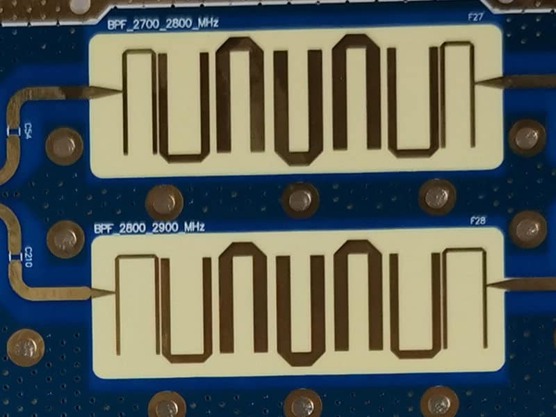
An HDI RF Board is a sophisticated printed circuit board that merges High-Density Interconnect technology with specialized materials and design rules to excel in radio frequency applications. Pushing the limits of modern wireless, radar, and sensing systems demands circuits that are faster, smaller, and more reliable than ever. This article provides a comprehensive guide to understanding HDI RF boards, their advantages for high-frequency designs, key structural elements, cost considerations, comparisons with other substrates, and guidance on selecting a reliable HDI PCB manufacturer.
Are your current PCB solutions holding back your next-generation RF design? You might be facing these common challenges:
Signal Degradation at High Frequencies: Standard PCB constructions struggle with significant signal loss, crosstalk, and impedance discontinuities, crippling the performance of sensitive RF and microwave circuits.
Size and Weight Constraints: Achieving complex functionality often means larger, multilayer boards that contradict the miniaturization goals of modern portable and aerospace electronics.
Thermal Management Headaches: Dense component placement and high-power RF sections generate concentrated heat that standard boards cannot effectively dissipate, leading to reliability risks.
Prototyping and Yield Frustrations: Complex RF designs often require multiple expensive prototype iterations, and manufacturing defects in fine features can lead to poor yield and project delays.
Supply Chain and Expertise Gaps: Finding a manufacturer with both advanced HDI technology in PCB fabrication and deep RF/microwave design support is difficult, leading to communication breakdowns and suboptimal results.
The solution lies in partnering with a specialist who masters the fusion of HDI fabrication and RF principles. At BEST Technology, we engineer Premium HDI RF Boards specifically to overcome these hurdles.
Superior Signal Integrity: We utilize advanced HDI layer stacking, low-loss materials, and precise impedance control to ensure clean, high-fidelity signal transmission for your RF and microwave circuit boards.
Enabled Miniaturization: Our expertise in microvias and fine-line patterning packs more functionality into a smaller footprint, crucial for compact HDI Electronics and antenna systems.
Enhanced Thermal & Mechanical Reliability: We integrate thermal management strategies and robust stack-up designs from the start, ensuring your board remains stable and reliable under operational stress.
DFM-Driven Process & High Yield: Our design-for-manufacturability review and controlled processes reduce prototyping cycles and ensure high production yield, even for complex designs like HF RFID antenna modules.
One-Stop Expert Partnership: As a leading HDI RF Board manufacturer, EBest Circuit (Best Technology) provides end-to-end support—from material selection and design review to advanced fabrication and testing—simplifying your supply chain.
BEST Technology is a premier specialist in manufacturing advanced printed circuit boards, with over 19 years of expertise in HDI PCB and high-frequency solutions. We combine state-of-the-art production facilities with profound technical knowledge to serve clients in telecommunications, aerospace, defense, and medical industries. We are not just a HDI PCB manufacturer; we are your technical partner in realizing cutting-edge HDI RF designs and solutions. For inquiries, pls feel free to contact us at sales@bestpcbs.com.
What Is an HDI RF Board?
At its core, an HDI RF Board is defined by the application of High-Density Interconnect (HDI) methodologies to boards operating at radio frequencies. To understand the HDI PCB definition, it is a board with a higher wiring density per unit area than conventional PCBs, achieved through features like microvias (laser-drilled), fine lines and spaces, and sequential lamination. When this is applied to RF designs, it involves using specialized low-loss laminate materials (like Rogers, Taconic) alongside these HDI techniques.
How HDI RF Circuit Board Differs from Standard High-Frequency Designs? Here’s how it differs from standard RF boards:
Interconnect Density: Standard RF boards often use larger through-hole vias, limiting routing space. HDI RF boards employ microvias (often blind and buried), allowing escape routing from dense RF ICs (like BGAs) and more efficient layer transitions.
Material Integration: While both may use similar high-frequency laminates, HDI RF boards require materials that are also compatible with the multiple lamination cycles and fine-feature etching of HDI processes.
Design for Performance and Size: A standard design might increase board size to accommodate components and routing. An HDI RF design optimizes both electrical performance (shorter, controlled paths) and physical size simultaneously.
Manufacturing Complexity: The fabrication of HDI RF boards is significantly more complex, requiring precise control over dielectric thickness, via formation, and copper profiling to maintain consistent RF characteristics.
In summary, an HDI RF board is the strategic convergence of miniaturization technology (HDI) and high-frequency engineering, creating a platform that is superior for modern, compact, and high-performance wireless devices.
Why HDI Technology in PCB Matters for RF Performance?
The role of HDI technology in PCB fabrication is transformative for RF applications. It directly addresses the critical demands of high-frequency circuits.
Minimized Signal Path Length: Shorter traces between components, enabled by dense interconnects, reduce signal delay, propagation loss, and the chance of picking up noise.
Improved Impedance Control & Signal Integrity: The fine-line capabilities of HDI allow for precise control over trace width and spacing, which is paramount for maintaining consistent characteristic impedance (e.g., 50Ω) across the board, minimizing reflections.
Reduced Parasitic Effects: Microvias have lower parasitic capacitance and inductance compared to traditional through-hole vias. This is crucial at GHz frequencies, where via stubs can act as antennas or cause resonances.
Enhanced Grounding and Shielding: Multiple buried vias can create a dense via fence or a coaxial-like shielding structure around sensitive RF lines, effectively containing electromagnetic interference (EMI) and crosstalk.
Facilitation of Advanced Packaging: HDI is essential for integrating embedded passive components (resistors, capacitors) and for fan-out routing from advanced semiconductor packages, keeping the entire RF front-end compact and efficient.
For RF performance, HDI is not just about making the board smaller; it’s about making it electrically superior by reducing negative effects intrinsic to larger, conventional geometries.
Key Structure and HDI Layer Configurations Used in Advanced RF Modules and Antenna Systems
The architecture of an HDI RF board is its blueprint for success. The HDI layer build-up is carefully planned to meet electrical and mechanical goals.
Standard “1+N+1” to “Any Layer” Build-Ups: Simple HDI starts with “1+N+1” (one HDI layer on each side of a core). Advanced RF modules may use “2+N+2” or “any layer” HDI, where almost every layer can be connected with microvias, offering maximum design flexibility for complex HDI Electronics.
Hybrid Material Stack-ups: A common configuration uses a high-performance, low-loss RF laminate (e.g., Rogers 4350B) for critical signal layers, bonded with standard FR-4 prepreg for other layers. This optimizes cost and performance.
Buried and Blind Via Structures: Critical RF lines often reside on outer layers for best performance. Blind vias connect surface layers to adjacent inner layers without going through the entire board, preserving space and reducing stub length.
Via-in-Pad and Filled Vias: To further miniaturize, vias are placed directly in component pads. These are plated and filled with conductive or non-conductive material, creating a flat surface for soldering and excellent thermal conduction for components like power amplifiers.
Shielding Cavities and Antenna Structures: HDI processes can create milled cavities for shielding cans or precise, multi-layer antenna structures like patch antennas for HF RFID antenna systems, all integrated within the board itself.
This sophisticated layering is what allows a single, compact HDI RF Board to function as an entire RF subsystem.
What is HDI RF Board Price?
The HDI RF board price is not a fixed number but a variable determined by a confluence of technical factors. Understanding these helps in budgeting and design optimization.
Board Complexity: This is the primary driver. More sequential lamination cycles, a higher count of laser-drilled microvias, and “any layer” capability increase cost significantly.
Material Selection: High-frequency laminates (Rogers, Taconic, etc.) are far more expensive than standard FR-4. The percentage of these materials in the hybrid stack-up directly impacts the raw board cost.
Layer Count and Size: More layers and a larger board area naturally increase material and processing time. HDI allows for smaller sizes, which can offset the cost of increased layer count.
Specialized Processes: Costs for via-in-pad, filled vias, tight impedance control tolerances (e.g., ±5%), and advanced surface finishes (ENEPIG) add to the final price.
Order Volume and Turnaround Time: Prototype quantities have a higher cost per unit. Production volumes bring economies of scale. Expedited fabrication also carries a premium.
As a rough guideline, expect an HDI RF board to cost 2 to 5 times more than a standard FR-4 PCB with the same dimensions and layer count, primarily due to materials and process complexity. The investment, however, is justified by the unparalleled performance and integration it enables.
Comparing HDI Electronics with Flex PCB, LED PCB, and Other Specialized Substrates for RF Applications
Choosing the right substrate is critical. Here’s how HDI Electronics compare:
HDI RF Board vs. Flex PCB: Flex boards offer dynamic bending and space savings in assemblies. However, for core RF circuitry, standard flex materials often have higher loss tangents. HDI rigid boards provide better rigidity for component support, superior thermal management, and wider availability of ultra-low-loss laminate options. They are often used together (Rigid-Flex) where HDI areas handle the core RF processing.
HDI RF Board vs. Standard LED PCB: A typical LED PCB prioritizes high thermal conductivity (using metal core like Aluminum) and simple circuitry to drive LEDs. An HDI RF board is focused on signal integrity at high frequencies, using different materials and complex, controlled-impedance routing. Their purposes are distinct.
HDI RF Board vs. Standard FR-4 Multilayer: Standard multilayer boards lack the fine features and low-loss materials. They are unsuitable for high-frequency performance but are cost-effective for digital and low-frequency analog sections. HDI RF is the specialized choice for the RF front-end.
HDI RF Board vs. Pure Ceramic Substrate (e.g., Alumina, LTCC): Ceramic offers excellent thermal performance and very fine features but at a very high cost and limited size. HDI RF on organic laminates provides a better balance of performance, size, design flexibility, and cost for most RF applications below the millimeter-wave extreme.
In essence, for the heart of a high-frequency system—where signal integrity, miniaturization, and integration are non-negotiable—the Premium HDI RF Board is the unmatched solution.
How HF RFID Antenna, RFI Board, and RDI Board Designs Benefit from HDI Technology?
These specialized applications gain distinct advantages:
HF RFID Antenna: It is short for High Frequency Radio Frequency Identification Antenna. HF RFID antenna coils often require precise, multi-turn patterns. HDI technology allows these coils to be fabricated with extreme accuracy as embedded planar structures within the board layers, improving reliability and enabling integration with the control chip in a single, slim package. Application: Operating at the 13.56 MHz HF band, these HDI-enabled antenna inlays or modules are critical for contactless payment systems (e.g., credit cards, mobile wallets), secure access control badges, library item tracking, and high-security document authentication.
RFI (Radio Frequency Interference) Board: Boards designed to mitigate RFI need excellent shielding. HDI allows for the easy creation of dense ground via fences and shielded cavities between noisy and sensitive sections directly within the board structure, providing superior isolation compared to external shields. Application: Crucial for applications across a wide frequency spectrum, these boards are used in sensitive medical imaging equipment (MRI), high-density telecom infrastructure, aerospace avionics, and advanced test & measurement instruments to prevent signal degradation and ensure regulatory EMI/EMC compliance.
RDI (Research, Development, and Innovation) Boards: Prototype and RDI board projects for cutting-edge technology benefit immensely from HDI’s flexibility. It allows researchers to pack sensors, RF components, and digital processors into a small form factor for proof-of-concept devices, accelerating innovation cycles. Application: : Used in prototyping next-generation IoT devices, millimeter-wave (mmWave) communication systems (e.g., 5G/6G fronthaul), phased array radar elements, and quantum computing interfaces, where form factor, signal integrity, and rapid design iteration are paramount.
In all cases, HDI provides the design freedom and performance consistency needed to turn advanced concepts into reliable, manufacturable products.
How to Select Reliable HDI RF Board Manufacturers?
Choosing the right partner is as important as the design itself. Look for these traits in HDI RF board manufacturers:
Proven Technical Expertise: They must demonstrate a deep understanding of both HDI processes and RF principles (impedance, loss, materials).
Advanced Manufacturing Capability: Verify they have laser drilling, precision lamination, and electrical testing equipment (like network analyzers) specifically for RF parameters.
Material Partnerships: Access to a wide range of certified high-frequency laminates from leading suppliers is essential.
Design Support Services: The best manufacturers offer upfront engineering support, including stack-up design, simulation assistance, and thorough DFM analysis.
Quality and Certifications: Look for relevant industry certifications (ISO, IATF 16949, AS9100 for aerospace) and a robust quality management system.
Why Choose BEST Technology as One of Your Best HDI PCB Manufacturers for RF and Microwave Circuit Boards?
BEST Technology stands out by fulfilling all the above criteria and more. We specialize in the niche intersection of HDI and high-frequency, offering:
Dual Expertise: Our engineers are fluent in the language of both advanced fabrication and RF design.
State-of-the-Art Facility: Equipped with specialized lines for handling low-loss materials and achieving tight tolerances.
End-to-End Partnership: We collaborate from the early design stage through prototyping to volume production, ensuring your RF and microwave circuit boards are not only designed well but are also optimized for manufacturability and yield.
Commitment to Reliability: Every Premium HDI RF Board we build undergoes rigorous testing to meet the stringent requirements of high-reliability applications. And our PCB and SMT factory is fully compatible with ISO 9001, ISO 13485, IATF 16949, AS9100D, UL, REACH, and RoHS.
Short Lead Times: We operate dedicated, streamlined production lines and maintain strategic raw material partnerships. This optimized workflow, combined with our deep process expertise, allows us to offer industry-leading turnaround times for both complex prototypes and volume production, enabling you to accelerate your product development and meet critical market windows without compromising on quality.
All in all, an HDI RF Board represents the pinnacle of integration for high-frequency electronics, combining the miniaturization power of HDI with the performance demands of RF circuits. This guide has explored its HDI PCB definition, benefits, structures, costs, and ideal applications to help you leverage this advanced technology for your most demanding projects.
Success in this field requires a manufacturer that is more than a fabrication house; it requires a technical co-innovator. BEST Technology brings nearly two decades of specialized HDI RF circuit board experience, cutting-edge capabilities, and a partnership-driven approach to every HDI device project. Pls feel free to contact us for a consultation or quote via sales@bestpcbs.com
FAQs
Q: What is the difference between HDI PCB and regular PCB?
A: The main differences are density and construction. HDI PCBs use microvias (typically <150µm), finer traces/spaces, and often sequential build-up to achieve much higher interconnection density in a smaller area compared to regular PCBs that rely on larger through-hole vias and simpler lamination.
Q: What are the benefits of HDI PCB?
A: Key benefits include significant size and weight reduction, improved electrical performance (faster signals, less noise), enhanced reliability (fewer mechanical interconnections), and the ability to accommodate advanced, high-pin-count components like BGAs.
Q: What are the 4 tiers of HDI?
A: HDI complexity is often categorized into tiers:
Tier 1: 1+N+1 (Microvias on one side of the core).
Tier 2: 2+N+2 (Microvias on both sides, potentially with stacked vias).
Tier 3: 3+N+3 (Multiple layers of stacked microvias).
Tier 4 & Above: Also called “Any Layer” HDI, where microvias can connect any two adjacent layers throughout the board stack-up.
Q: What is the process of HDI PCB fabrication?
A: It involves sequential lamination cycles. Key steps include: imaging and etching of fine inner layers, laser drilling of microvias, via metallization (plating), layer alignment and bonding (lamination), and repeat. This differs from standard PCB fab which often uses a single lamination of all layers followed by mechanical drilling of through-holes.
Q: What is an HDI device?
A: In the context of PCBs, an “HDI device” typically refers to the final electronic product or module that is enabled by or built upon an HDI printed circuit board, such as a smartphone, a satellite communication module, or a medical imaging device.
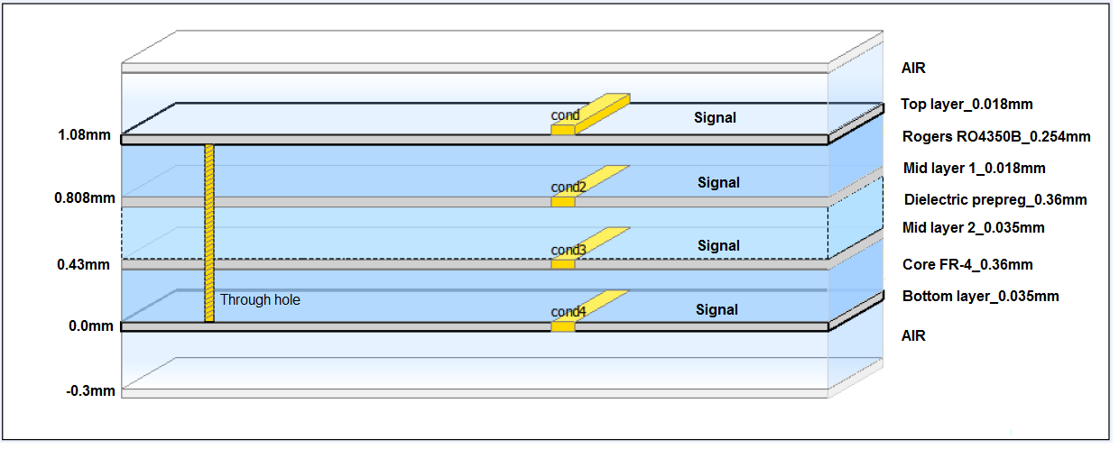
If you are working on RF or microwave PCB design, the material you choose directly impacts signal loss, phase stability, thermal performance, and overall system reliability. Rogers RO4350B is one of the most widely used high-frequency laminates in telecom, radar, 5G, satellite, and advanced wireless systems. This guide provides a complete breakdown of RO4350B datasheet properties, thickness options, RF advantages, and a comparison against FR4—plus practical manufacturing notes for PCB engineers.
What Is Rogers RO4350B Material?
Rogers RO4350B is a hydrocarbon-ceramic, glass-reinforced laminate engineered for RF and microwave applications from the Rogers RO4000® series. Unlike PTFE-based laminates, RO4350B can be fabricated using standard FR4 PCB processes—a huge benefit for cost, lead time, and manufacturability—while still delivering excellent electrical stability at GHz frequencies.
Key characteristics:
Dk = 3.48 ± 0.05 (10 GHz, z-axis)
Df ≈ 0.0037 (low loss)
High thermal stability
Low moisture absorption (<0.06%)
Compatible with FR4 processes
Excellent for hybrid stack-ups
What Is Rogers RO4350B Material?
What Is RO4350B Used for in RF PCB Applications?
RO4350B is found in nearly every modern RF system. Typical uses include:
5G antennas and base-stations
Phased-array radar modules
LNA, PA, and front-end RF chains
Power amplifiers requiring robust thermal paths
Filters, couplers, baluns, and RF matching networks
Automotive ADAS radar
Satellite communication modules
High-performance mixed-signal and RF/digital hybrid boards
Because it balances cost and performance, RO4350B is ideal for mid-to-high volume RF production.
Rogers RO4350B Datasheet: Full Material Properties Overview
Below is a consolidated summary of all essential RO4350B datasheet values RF engineers frequently use in simulation, stack-ups, and manufacturing notes.
RO4350B’s thermal conductivity of 0.69 W/m·K is significantly higher than typical FR4 (~0.3 W/m·K).
This means:
Better heat spreading
Higher reliability under RF power loads
Improved board life during thermal cycles
Lower risk of delamination
This makes RO4350B a strong candidate for RF power amplifiers and modules with high current density.
RO4350B Thickness Options & Common Stack-Up Selections
RO4350B thickness availability is wide, giving designers flexibility.
Common RO4350B Thicknesses
0.101 mm / 0.004”
0.203 mm / 0.008”
0.254 mm / 0.010”
0.3048 mm / 0.012”
0.406 mm / 0.016”
0.508 mm / 0.020”
0.813 mm / 0.032”
1.524 mm / 0.060”
Copper options: ½ oz, 1 oz, 2 oz.
Common Stack-up Approaches
1. RF-only board:
Single RO4350B core for antennas, filters, or couplers.
2. Hybrid stack-up (RO4350B + FR4):
RF layers on RO4350B
Digital/Power layers on FR4
Best cost-performance balance
3. Multilayer RO4350B stack-up:
For radar, high-power, or mmWave systems requiring uniform RF behavior.
RO4350B vs FR-4: Differences in RF Performance
FR-4 is a good general-purpose material but struggles at higher RF bands. Its dielectric constant shifts with humidity, temperature, and frequency. Loss levels rise significantly above 1–2 GHz, which affects range, efficiency, and signal clarity.
RO4350B addresses these issues with stable electrical behavior, low loss, and stronger control of impedance.
Feature
RO4350B
FR-4
Dk Stability
Very stable
Unstable at high frequency
Loss (Df)
Low
High
High-frequency use
Excellent
Limited
Thermal stability
Strong
Moderate
RF performance
Consistent
Varies widely
Typical use
RF, microwave, antennas
General electronics
For RF paths, RO4350B is nearly always the better choice.
Rogers 4000 Series Materials Overview
The RO4000® series includes hydrocarbon-ceramic laminates designed for RF and microwave work. The series offers stable dielectric values, low moisture absorption, and predictable performance across frequency ranges. These materials support antennas, filters, couplers, radar units, medical sensors, and industrial communication systems. RO4003C and RO4350B are the most common choices, though other variants exist for special electrical or mechanical needs. Here are some other RO4000® series materials:
Which Rogers Materials Can Be Used for RF & Microwave PCB?
Common Rogers RF materials include:
RO4350B – balanced performance, processable like FR4
RO4003C – lower loss, great for 10+ GHz
RO4835 – improved oxidation resistance and stability
RT/duroid® series – PTFE-based ultra-low-loss materials for mmWave
TMM® series – ceramic thermoset laminates for precision high-power RF
Choose based on frequency, thermal load, and tolerance requirements.
RO4350B PCB Manufacturing Considerations
Although RO4350B is easier to manufacture than PTFE materials, achieving consistent RF performance requires following specific process guidelines. Here are the key considerations for PCB fabrication:
RO4350B PCB Manufacturing Considerations
1. FR4-compatible processing, but with controlled parameters
RO4350B supports standard PCB processes, but drill speeds, lamination pressure, bake profiles, and final copper thickness must be carefully controlled to ensure stable impedance and dielectric consistency.
2. Hybrid stack-ups require expert lamination control
When combining RO4350B with FR4, differences in CTE (coefficient of thermal expansion) must be managed to avoid warpage, resin starvation, or delamination. Precise prepreg selection and lamination cycles are essential.
3. Accurate impedance control is critical
RF designs often require ±5% or tighter impedance tolerance. Manufacturers must account for:
RO4350B’s ceramic-filled structure requires optimized drill parameters to prevent smear and maintain high hole-wall quality, ensuring reliable via plating for multilayer RF PCBs.
5. Proper material storage and handling
To prevent moisture absorption and dimensional shift, the material should be kept in a dry, controlled environment and baked before lamination when necessary.
With these practices, RO4350B PCBs can achieve repeatable RF performance from prototype to mass production.
Why EBest Circuit (Best Technology) Is Preferred for RO4350B PCB Fabrication?
When working with RO4350B, choosing the right PCB manufacturer is critical. EBest Circuit (Best Technology) is trusted by RF engineers because:
They stock RO4350B in multiple thicknesses
Provide RF stack-up simulation support
Offer tight impedance control with test coupons
Perform high-precision routing and controlled-depth milling
Support hybrid RO4350B + FR4 multilayers
Provide material certifications and Rogers-lot traceability
If you need consistent RF performance from prototype to mass production, EBest Circuit (Best Technology) is a reliable partner for RO4350B PCB fabrication.
FAQs
1. Does RO4350B support buried or blind vias in multilayer RF boards?
Yes. RO4350B works well in multilayer designs that use blind or buried vias. Its mechanical strength and low z-axis expansion help maintain via reliability during lamination and thermal cycling. When designers use selective RO4350B layers inside a hybrid stack-up, careful lamination scheduling helps control movement and keep impedance stable.
2. Is RO4350B compatible with ENIG, immersion silver, or HASL finishes?
Yes. RO4350B supports common surface finishes, including ENIG, immersion silver, OSP, and certain types of lead-free HASL. Most RF boards use ENIG or immersion silver because these finishes give cleaner surfaces, consistent thickness, and smoother trace edges. A smooth finish helps reduce signal loss at high frequencies. HASL may be less preferred for controlled-impedance lines due to its uneven surface.
3. Can RO4350B be used for power amplifiers that generate heavy heat?
Yes. Many PA modules run on RO4350B because it handles heat better than FR-4 and holds impedance during thermal loads. Designers still need good thermal paths, such as thermal vias under power devices or metal backers for heat spreading. If the PA generates extreme heat, ceramic or metal-backed constructions may be considered. For most communication-grade PAs, RO4350B provides more than enough stability.
4. What stack-up mistakes should designers avoid when using RO4350B?
A common mistake is mixing RO4350B and FR-4 without modeling the transition area. The shift in dielectric constant affects line impedance if the transition is not controlled. Another mistake is routing sensitive RF lines too close to ground via fences, which can create unintended coupling. Over-constraining solder masks around RF traces may also shift the effective dielectric environment.
5. Is RO4350B more expensive than FR-4, and how does it impact project cost?
Yes, RO4350B costs more than FR-4 due to its electrical stability and engineered formulation. The material price is higher, and multilayer stacks may need tighter controls. However, the overall project cost can still drop because fewer design spins occur, RF tuning time is reduced, and system performance becomes more predictable. In many RF designs, the ROI justifies the material cost.
Looking for aPCB manufacturer in Singapore? If you are searching for a custom PCB manufacturer in Singapore, this guide explains the common challenges in this region and how a trusted partner can provide stable quality and faster delivery.
Are You Facing these Problems in Singapore PCB Customization?
Insufficient prototyping accuracy leading to R&D rework? How to avoid the risk of subtle circuit short circuits/open circuits and prevent delays of over 30% in product launch cycles?
Small-batch orders rejected? High minimum order quantities increase costs for startup teams by 50%, yet there are no alternative solutions?
Difficulty in implementing design solutions? Lack of DFM analysis leads to pad defects, requiring secondary modifications and delaying the crucial product launch period?
Unstable quality in high-end PCB production? Yield fluctuations in high-density HDI boards and flexible circuits – how to meet the stringent requirements of medical/automotive grades?
Unreliable delivery commitments? Delays cause downstream production line shutdowns and losses – how to ensure high on-time delivery?
Our PCB Solutions to these Problems
High-precision sampling to break R&D Difficulties: Advanced laser drilling technology supports 1-64 layer PCB sampling with a minimum line width/spacing of 0.075mm±0.01mm matching micro-component soldering needs. Each batch includes free signal integrity analysis reports and X-ray inspections to proactively avoid 99% of potential defects and reduce R&D cycles by 40%.
Zero-threshold small batch customization: No minimum order quantity restrictions—enjoy mass production-grade processes starting from 1 piece. For startups, we offer cost-sensitive schemes that reduce per-piece costs by 35% (approximately $5 USD/piece) through material panel optimization. Supports fine soldering like BGA ball placement and QFN packaging for consumer electronics/IoT validation needs.
Free DFM design optimization to ensure landing: Complimentary professional DFM analysis automatically verifies 18 parameters including trace layout and impedance control. Optimized schemes show significant improvement in first-pass success rates reducing average client design iterations by 2 times and saving over $20K USD per project in R&D costs.
Authoritative certifications for high-end manufacturing capabilities: Mastered high-density HDI (minimum blind/buried via 0.1mm), rigid-flex boards (bend radius ≤1mm), and high-frequency material processes. Certified with ISO 9001, IATF 16949 automotive grade, medical ISO 13485 standards—products meet 5G base stations, surgical robotics and other demanding scenarios with yield stability above 99.8%.
Guaranteed delivery control across the entire process: Standard orders delivered in 7-10 business days with 24-hour expedited sampling for urgent needs. On-time delivery rate reaches 99%. For delayed orders we activate a double compensation mechanism paired with dedicated customer service for 48-hour on-site resolution of unexpected issues.
Why Choose EBest Circuit (Best Technology) for Global PCB Manufacturer?
Reasons Why Choose EBest Circuit (Best Technology) for Global PCB Manufacturer:
Comprehensive certification coverage: Holds ISO 9001 IATF 16949 RoHS 2.0 and medical ISO 13485 certificates meeting European-American environmental safety mandates.
19 years of PCB manufacturing expertise: Served 600+ global enterprises built a production error database and saved clients 18% average rework costs through process improvements.
Competitive pricing without hidden cost: Global supply chain integration provides 15%-20% below market average quotes with tiered pricing for cost-sensitive projects.
24-hour rapid prototyping for urgent orders Dedicated fast-track lines support 24-hour turnaround from file review to finished product for urgent prototyping and exhibition needs.
Full-inspection quality control: Each PCB undergoes triple verification via AOI automated optical inspection fly-probe testing and manual final checks achieving 99.8% pass rates with traceable quality reports attached.
Free DFM optimization: Expert teams provide complimentary manufacturability analysis to preempt 90% of design flaws and reduce post-modification costs.
Flexible service models: Supports full-stage needs from 1-piece prototypes to 100k+ volume production with value-added services like custom packaging and specialty logistics.
Support customization solutions: Including raw material customization, surface treatment customization, solder mask customization, and many other service types.
Welcome to contact us if you have any issues about PCB design, prototyping, mass production and assembly: sales@bestpcbs.com.
List of PCB Manufacturers in Singapore
1. Circuits Plus Pte Ltd
Main business: PCB manufacturing for industrial and electronic equipment.
Lead time: 2-6 weeks (includes design validation + production phases).
Custom Service Types Offered by Singapore PCB Manufacturers
High-precision prototype customization: For R&D phase needs, provides small-batch (1-100 units) high-precision PCB prototyping with rapid iteration support to shorten development cycles.
High-density PCB customization: Meets 5G & AI device requirements via ≤0.1mm line/space high-density PCB production, enhancing component integration and signal efficiency.
Special material customization: Offers tailored PCBs using ceramic substrates, aluminum CCL, polyimide flexible materials for extreme conditions (high temp/humidity/flexure).
Industry-specific customization: Delivers dedicated solutions for automotive (AEC-Q grade heat-resistant PCBs), medical (biocompatible PCBs), industrial control (EMI-resistant PCBs).
Surface finish customization: Provides HASL, immersion gold, ENIG, OSP and other finishes to address diverse soldering and oxidation protection needs.
Integrated assembly customization: Combines PCB manufacturing with component sourcing, SMT assembly for “one-stop” delivery, reducing supply chain management costs.
Aesthetic & packaging customization: Supports PCB color, silkscreen marking, contour routing, plus ESD/moisture-resistant packaging for secure transit.
Eco-compliance customization: Uses RoHS/REACH-compliant materials (lead-free solder, eco-substrates) and processes to meet global environmental regulations.
How to Choose the Right PCB Manufacturer in Singapore?
Prioritize International Authoritative Certifications: Select manufacturers certified with ISO 9001 (Quality Management), ISO 14001 (Environmental Management), UL (US Safety Certification), IPC Standards (Association Connecting Electronics Industries), and RoHS/REACH compliance. These certifications serve as the default “quality benchmark” for European and American clients.
Specialized Process Certifications: For niche areas like high-frequency high-speed boards, HDI (High-Density Interconnect), rigid-flex boards, verify certifications such as NASA, AS9100 (Aerospace), or IATF 16949 (Automotive), demonstrating technical depth.
2. Technical Capability and Capacity Alignment
Equipment and Process Transparency: Request a list of production line equipment (e.g., LDI Laser Direct Imaging, VCP Vertical Continuous Plating, AOI Automated Optical Inspection) and process parameter ranges (line width/spacing accuracy, layer count capability, minimum hole size) to ensure alignment with project requirements.
Rapid Prototyping and Small Batch Capability: European-American clients often require fast design validation. Choose manufacturers offering 24-48 hour rapid prototyping and small batch delivery within 7 days to shorten R&D cycles.
Material Supply Chain Transparency: Confirm key material brands (e.g., Panasonic M-Series, Shengyi Technology high-frequency materials) and traceability for substrates, solder masks (e.g., Taiyo Ink), avoiding substandard substitution risks.
3. Client Case Studies and Industry Reputation
Verify Case Authenticity: Request references to past European-American client projects (e.g., German industrial control, US medical devices, Singapore 5G communications). Validate technical challenges solved (e.g., impedance control, thermal design) and final product performance.
Third-Party Evaluations: Cross-reference delivery punctuality, yield rates, and after-sales responsiveness through industry forums (EE Times, EDN), supply chain rating platforms (Dun & Bradstreet), or independent audit reports.
4. Communication and Collaboration Efficiency
Multilingual Support and Immediate Response: Engage manufacturers with multilingual teams (English/German/French) ensuring seamless design communication, technical issue feedback, and order status updates within 24 hours (European-American working hours).
Digital Collaboration Tools: Prioritize manufacturers using direct EDA file integration (Altium, OrCAD), online quoting systems, and real-time production tracking platforms (ERP/MES integration) for enhanced collaboration efficiency.
5. Cost Efficiency and Long-Term Partnership
Transparent Pricing and Cost Analysis: Request itemized quotes (material costs, processing fees, testing, shipping) and compare cost differentials between Singapore and Southeast Asian neighbors (Malaysia, Thailand). Clarify the added value of “Made in Singapore” (technical premium, logistics convenience).
Long-Term Cooperation Mechanisms: Establish annual framework agreements defining price lock-in periods, priority capacity guarantees, and technology sharing (e.g., new material applications, process optimization) to mitigate long-term risks.
6. Environmental and Sustainability Practices
Green Production Commitments: Confirm adoption of lead-free processes, wastewater treatment systems, energy-efficient equipment (LED curing), and published carbon footprint data to meet European-American ESG procurement requirements.
Circular Economy Measures: Assess support for old board recycling and material reuse programs, reflecting emphasis on resource efficiency.
7. Site Visits and Risk Mitigation
Factory Site Audits: For critical projects, arrange on-site inspections focusing on production environment (cleanroom class), quality control processes (first-article inspection, outgoing quality checks), employee training records, and safety protocol compliance.
Third-Party Audit Options: If on-site visits are infeasible, commission international agencies (SGS, TÜV) for remote audits and detailed evaluation reports to inform decision-making.
How to Evaluate Production Capacity of PCB Manufacturers in Singapore?
1. Evaluate production equipment setup: Check for advanced equipment like high-precision laser drills, automated etching lines, and AOI inspection systems, equipment sophistication directly impacts manufacturing precision.
2. Confirm capacity scale: Inquire about peak/monthly capacity and maximum concurrent order capacity to align with long-term/batch needs.
3. Assess process coverage: Verify capability to produce PCBs of varying layers, materials, structures, and handle complex techniques like fine-pitch soldering or blind/buried vias.
4. Review technical team expertise: Gauge engineer team size, experience, and backgrounds—critical for tackling custom tech challenges and DFM optimization.
5. Analyze raw material supply chain: Ensure stable partnerships with global suppliers of premium substrates (e.g., FR-4) and copper foil, raw material quality underpins production capability.
6. Examine production standardization: Check for standardized SOPs across operations to minimize quality variance from human factors.
7. Understand capacity flexibility: Assess ability to scale production or handle urgent orders amid demand fluctuations.
8. Validate quality consistency: Request 3-6 months of yield rate data and customer-reported defect stats to evaluate process control.
How to Evaluate Lead Time of PCB Manufacturing Companies in Singapore?
1. Clarify standard lead time benchmarks: Request lead time tables for different PCB types (e.g., single-layer, multi-layer, flexible) as reference.
2. Understand production scheduling system: Check if orders are managed via digital systems with real-time status tracking to avoid manual scheduling errors.
3. Verify urgent order handling: Confirm priority tiers, capacity buffers, and minimum turnaround for rush orders.
4. Assess supply chain coordination efficiency: Evaluate component sourcing timelines (if outsourced) and logistics models impacting overall lead time.
5. Confirm progress communication protocol: Define update frequency (daily/weekly) and format (system alerts/emails) for transparency.
6. Review on-time delivery history: Request last 6 months’ OTIF (on-time-in-full) data to assess actual vs. promised lead times.
7. Define delay mitigation terms: Include liability and compensation clauses (e.g., daily deductions) in contracts to protect interests.
8. Evaluate force majeure preparedness: Inquire about contingency plans for supply shortages or equipment failures to gauge risk resilience.
Frequently Asked Questions
Q1: PCB prototypes deviate from design drawings, affecting assembly? A1: Choose manufacturers supporting DFM pre-analysis. Before placing orders, professional engineers conduct manufacturability reviews of design drawings to correct layout, hole positions, etc., in advance. After prototyping, detailed inspection reports are provided to ensure consistency with drawing parameters.
Q2: Small-batch orders frequently experience delivery delays and poor communication feedback? A2: Prioritize manufacturers with dedicated customer service mechanisms and assign clear order follow-up personnel. Sign contracts with delivery guarantee clauses requiring regular production progress updates. In case of delays, provide clear reasons and resolution measures.
Q3: PCB products exhibit instability in high-temperature environments? A3: Specify the product’s operating temperature range when ordering. Manufacturers recommend high-temperature-resistant substrates (e.g., high-Tg FR-4) and corresponding processes. Conduct high-temperature environmental simulation testing post-production to ensure compliance with usage requirements.
Q4: Partial PCB electrical performance fails to meet standards during mass production? Solution: Select manufacturers with full-process quality inspection systems and request batch sampling reports. In case of issues, the manufacturer must respond within 24 hours, analyze failure causes, provide return/replacement/replenishment solutions, and bear associated losses.
Q5: Complex design schemes raise uncertainty about mass production feasibility? A5: Seek manufacturers with experienced technical teams offering design evaluation services. First conduct small-batch pilot production to verify process feasibility and product stability before initiating mass production, reducing risks.
When designing RF and microwave PCBs, the laminate you choose directly affects insertion loss, impedance consistency, manufacturability, and long-term reliability. Among the many high-frequency materials from Rogers Corporation, RO4003C and RO4350B remain two of the most commonly used options across wireless, radar, and high-power RF hardware.
So, what is difference between RO4003C and RO4350B? Maybe you can find answer here. This guide breaks down how the two materials differ, how they perform electrically, what thickness options are available, and which material fits specific RF applications.
What Is Rogers RO4003C?
RO4003C is a glass-reinforced hydrocarbon ceramic laminate designed as a middle-ground option between standard FR-4 and more advanced microwave substrates. It was formulated to deliver excellent RF performance without the processing complexities associated with PTFE-based materials. Because its fabrication requirements align closely with FR-4, it has become a go-to material for mid-frequency wireless modules requiring predictable performance at a reasonable cost.
Material Composition
Hydrocarbon/ceramic-filled resin system
Woven glass reinforcement
PTFE-free formulation
Compatible with mainstream FR-4 manufacturing flows
This combination makes RO4003C easier to fabricate, more dimensionally stable, and more economical for medium-frequency applications, while still achieving significantly lower loss than FR-4.
Strengths
Lower insertion loss than FR-4, particularly above 2 GHz
Stable dielectric constant (~3.38) across temperature and frequency
No need for PTFE-type specialized drilling or etching
Widely available in multiple thicknesses and copper weights
Highly cost-effective for mid-range RF and mixed-signal applications
Limitations
Higher loss than RO4350B under high-power or high-frequency conditions
Somewhat reduced thermal reliability compared with RO4350B
Standard RO4003C does not carry a UL94 V-0 flame rating (except LoPro variants)
Best Suited For
RO4003C is ideal when you need solid RF performance without the cost or processing requirements of higher-end laminates:
2.4–10 GHz RF signal chains
IoT radios, compact wireless modules
Patch antennas, printed antennas, and small radar systems
LNAs, mixers, filters, RF front-end circuits
Its combination of affordability, consistency, and manufacturability has made it a staple material for mainstream RF electronics.
What Is RO4350B Material?
RO4350B is a flame-retardant hydrocarbon ceramic laminate engineered for high power, high reliability, and high-frequency RF systems. It delivers tighter dielectric control and improved thermal behavior compared with RO4003C.
Key Properties
Dk ≈ 3.48 (slightly higher than RO4003C)
Df ≈ 0.0037, supporting lower insertion loss at high power
UL94 V-0 flame-retardant rated
Higher thermal conductivity
Very tight Dk tolerance for precision RF designs
Higher Tg, improving stability during soldering and high-temp processing
Typical Use Cases
High-power RF amplifiers
5G, LTE, and small-cell base stations
Automotive radar (24 / 77 GHz)
Satellite and aerospace RF systems
Filters, couplers, and phased-array modules
RO4350B is ideal when electrical performance and thermal robustness are both critical.
RO4003C vs RO4350B: Electrical Performance Comparison
Although both materials belong to the same hydrocarbon ceramic family, their microwave performance differs in several meaningful ways.
Property
RO4003C
RO4350B
Notes
Dielectric Constant (Dk)
~3.38
~3.48
Higher Dk allows slightly smaller RF structures
Dissipation Factor (Df)
~0.0027
~0.0037
RO4350B performs better at high power; RO4003C wins at lower GHz
Thermal Conductivity
Lower
Higher
RO4350B dissipates heat more effectively
Temperature Stability
Good
Excellent
RO4350B is more stable outdoors and under load
Power Handling
Medium
High
RO4350B excels in power electronics
Insertion Loss
Good
Better
Particularly for long feedlines or high-power paths
Summary
RO4003C → balanced, economical, suitable for mid-frequency designs
RO4350B → precision-grade material designed for high power and extreme stability
RO4003C vs RO4350B: Thickness Options
Both laminates are available in a wide range of core thicknesses. However, their catalogs differ slightly, and RO4350B generally has tighter tolerances—important for controlled-impedance designs.
Common RO4003C Thicknesses
0.101 mm
0.203 mm
0.304 mm
0.508 mm
0.813 mm
1.524 mm
These options cover almost all mainstream antenna, filter, and RF routing needs.
Common RO4350B Thicknesses
0.101 mm
0.168 mm
0.254 mm
0.508 mm
0.762 mm
1.524 mm
RO4350B’s tighter thickness control results in more consistent RF behavior, especially in multi-layer microwave structures.
Is RO4003C Really Cheaper Than RO4350B?
In most real-world PCB quotations, RO4003C is indeed 10–25% cheaper than RO4350B. Yet the difference is not as large as engineers sometimes expect. RO4003C is less expensive because its resin does not include flame-retardant chemistry, its Dk tolerance is more forgiving, and its manufacturing process closely resembles FR-4. These factors reduce both the material price and the cost of PCB fabrication.
RO4350B’s higher cost comes from its UL94 V-0 rating, tighter dielectric tolerance, more stable thermal behavior, and more complex resin formulation. These advantages are essential in automotive radar, 5G systems, and aerospace electronics, where reliability and compliance requirements outweigh material cost. In small prototype runs, the price difference may be overshadowed by drill-time cost, impedance testing, or engineering setup fees. Therefore, while RO4003C is typically cheaper, the decision should still be guided by system-level performance rather than material cost alone.
When to Choose RO4003C and When to Choose RO4350B?
Selecting between the two laminates depends on frequency, power, environmental conditions, and regulatory constraints.
Choose RO4003C When:
operating frequency is below ~10 GHz
cost efficiency is a primary goal
fabrication simplicity is desired
power levels are moderate
the application is IoT, Wi-Fi/Bluetooth, radar front ends, or compact RF modules
Choose RO4350B When:
high power must be handled safely
stringent Dk tolerance is required
UL94 V-0 flame resistance is mandatory
operating frequency spans 10–40+ GHz
the application involves radar, satellite links, aerospace RF, or 5G infrastructure
RO4003C is best for mid-range systems, while RO4350B excels in harsh or precision-critical environments.
Key Fabrication Notes for RO4003C and RO4350B PCBs
tightly control dielectric thickness during lamination
ensure copper etching tolerance remains consistent for impedance control
use plasma cleaning to improve hole-wall quality
low-profile copper improves loss performance
avoid excessive lamination temperatures to protect resin integrity
select solder mask materials that do not absorb RF energy
Manufacturers experienced with Rogers laminates can reduce variability and ensure RF performance matches the design model.
RO4003C vs RO4350B vs FR4: Is Rogers Always Necessary?
FR-4 still plays an important role in RF design, especially where frequency demands are low and cost is a major constraint.
FR-4 Is Acceptable For:
sub-1 GHz circuits
low-precision RF systems
consumer electronics
Rogers Materials Are Required When:
insertion loss must be minimized
impedance variation must remain within ±5–10%
thermal stability is essential
high power or high frequency is involved
mmWave operation (24–77 GHz) is required
Quick Comparison
Material
Frequency Range
Loss
Cost
Best Applications
FR-4
<1 GHz
High
$
Basic RF
RO4003C
1–10 GHz
Medium-low
$$
Antennas, IoT, radar
RO4350B
10–40+ GHz
Low
$$$
5G, radar, high-power RF
FAQs About RO4003C and RO4350B
1. Can RO4003C replace RO4350B?
Yes, for sub-10 GHz and moderate-power designs, RO4003C can often replace RO4350B with minimal impact on performance.
2. Is RO4350B flame-retardant?
Absolutely. It is UL94 V-0 certified and widely accepted for telecom and aerospace hardware.
3. Which material has lower loss?
RO4350B generally performs better, especially in long RF traces or high-power paths.
4. Can FR-4 and Rogers be mixed in the same stackup?
Yes. Hybrid stackups are common in RF modules to balance cost and performance.
5. Which is better for antennas?
RO4003C suits most mid-frequency antennas; RO4350B is superior for high-power or outdoor antennas.
6. Which is better for 5G base stations?
RO4350B, due to its exceptional dielectric stability and flame resistance.
7. Do both support multilayer RF PCB structures?
Yes—with proper process control and experienced fabrication.
8. Are both suitable for mmWave?
RO4350B is the preferred option due to its lower loss and tighter tolerance.
9. Do they require special plating?
Standard plating works, but IPC-4103 guidelines are recommended for consistency.
PCB board colors refer to the solder mask hues applied to printed circuit boards, which not only enhance aesthetics but also serve critical functions like insulation and protection. This article explores the significance, processes, and quality aspects of PCB colors, offering insights for selecting the right options for your projects.
Are you struggling with inconsistent PCB color results or defects that impact performance? Common challenges include color variations, poor adhesion, and reliability issues. Below, we outline five key pain points faced by PCB buyers:
Inconsistent color coverage leading to uneven appearance.
Solder mask defects such as scratches or debris affecting functionality.
Difficulty in achieving precise color matching across batches.
Inadequate inspections resulting in undetected quality issues.
Limited process capabilities hindering complex designs.
To address these, BEST Technology provides robust solutions:
Strict process controls ensure uniform color application.
Custom color matching with high-resolution techniques.
Comprehensive inspections meet industry standards.
High-precision manufacturing supports diverse color requirements.
BEST Technology is a professional PCB and PCBA manufacturer with expertise in solder mask applications, leveraging state-of-the-art equipment and stringent quality checks to deliver reliable boards. Pls feel free to contact us at sales@bestpcbs.com for tailored solutions.
What Is the Color of a PCB Board?
The color of a PCB (Printed Circuit Board) board primarily refers to the color of the solder mask, a protective layer applied over the copper traces to prevent short circuits, reduce solder loss, and provide insulation.
Common PCB Colors and Their Features
Green Solder Mask:
Popularity and Cost: Green is the most widely used color because it is the cheapest and most readily available. It offers excellent reliability and is environmentally friendly, as it does not release toxic gases under high temperatures.
Manufacturing Advantages: In SMT (Surface Mount Technology) processes, green provides a good contrast for optical alignment during soldering, improving accuracy. Additionally, it minimizes issues like solder bridging, with a typical solder mask bridge width of 3mil for standard green boards.
Documentation Support: As noted in the materials, green is considered “common grade” and is less prone to problems such as color variation or handling difficulties compared to other colors.
Other Colors (e.g., Black, Blue, White, Red, Yellow):
Black Solder Mask:
Often perceived as high-end, black is challenging to manufacture because it absorbs UV light strongly during exposure, requiring a wider solder mask bridge (e.g., 4-6mil) to prevent defects.
This can lead to design constraints, such as larger pad spacing.
It is also less ideal for mass production due to higher rejection rates.
Blue Solder Mask:
Blue is considered novel and aesthetically pleasing but has several drawbacks.
Blue ink is more expensive (e.g., about 20 RMB/m² more for domestic blue ink than green), and it suffers from issues like lower hardness (making it prone to scratches), poor flow control (leading uneven coating), difficulty in hole plugging, longer baking times, and color changes after SMT.
These factors increase production costs and defect rates.
White Solder Mask:
White solder mask is widely used on metal-based PCBs, especially in LED and lighting applications, because of its excellent light reflectivity.
It enhances brightness and thermal performance by reflecting more light and reducing heat absorption from high-power LEDs.
Compared with darker solder mask colors, white provides a cleaner appearance and supports better optical efficiency in aluminum‐based and copper‐based board designs.
Red and Yellow Solder Masks:
Colors like red and yellow are used sparingly, often in niche products like IT devices without enclosures, but they share similar challenges with blue and black, such as variability in batch colors and higher sensitivity to process conditions.
In summary, PCB color choices depend on factors like aesthetics, cost, and application-specific needs. While green remains the recommended color among other colors.
Why Are Circuit Boards Green?
The solder mask, often called “green oil” in the industry, is essential for PCB functionality. While green is the most common color, accounting for over 90% of PCBs due to its cost-effectiveness and reliability, other colors like black, blue, red, white, and yellow are also used for specific applications, such as aesthetics or thermal management.
Green vs. Blue Solder Mask
Price:
Blue solder mask is more expensive—domestic blue ink costs about 20 RMB/m² more than green, while imported blue ink (e.g., Japanese) can be 100 RMB/m² higher.
This translates to a cost increase of 0.05–0.30 RMB per unit for products like DVD players.
Performance and Reliability:
Green ink is harder and more durable, reducing scratches and production defects.
Blue ink has higher fluidity, causing issues like oil accumulation and uneven coating, which require PCBs to be laid flat during production, occupying more space.
It also tends to discolor after SMT due to interactions with flux, and batch-to-color variation is common.
Manufacturing Considerations:
Blue ink requires longer baking times and is more susceptible to contamination, increasing complexity.
For example, solder mask bridging is harder to achieve with blue—typically needing a width of 3.5mil compared to 3mil for green, which affects design rules (e.g., pad spacing must be at least 7.5mil for blue vs. 7mil for green).
Human Factors:
Blue can cause more visual fatigue for assembly line workers compared to green, which is gentler on the eyes during prolonged inspections.
In summary, while PCB color choices depend on factors like aesthetics, cost, and application-specific needs, green remains the recommended color for most scenarios due to its cost-effectiveness, ease of manufacturing, and reliability. Other colors, such as blue or black, may suit high-end or specialized products but come with trade-offs in production stability and cost.
When selecting a color, designers should consider manufacturing capabilities, as illustrated in the case where black solder mask required adjustments to pad spacing to ensure solder mask bridges. Ultimately, green solder mask balances performance and economy, making it the industry standard.
What Silkscreen Machines Are Most Commonly Used Across Different PCB Colors?
Silkscreen machines are crucial for applying solder mask evenly. The most common types include:
Manual screen printers: These machines rely entirely on the operator for controlling the upward and downward movement of the screen frame, along with the pressure and motion of the squeegee. They are suitable for small batches or repair work but depend heavily on operator skill and consistency.
Semi-automatic screen printers: In these machines, loading and unloading the PCB are handled manually, while the printing stroke is mechanically controlled. Semi-automatic printers are widely used in PCB factories, including those at BEST Technology, because they deliver stable precision with higher efficiency than manual systems.
Full-automatic screen printers: By equipping a semi-automatic printer with automated feeding and output modules, it becomes a fully automatic screen printer. These systems support high-volume production, reduce labor dependency, and improve uniformity in solder mask or silkscreen application.
Across different PCB board colors, these machines help maintain consistent printing quality. Parameters such as screen tension, squeegee hardness, printing pressure, and ink viscosity can be fine-tuned to achieve optimal results for each color.
What Inspections Are Required for a Green Color PCB Board?
A green PCB board requires a comprehensive series of quality inspections to ensure its solder mask provides reliable electrical insulation, mechanical protection, and long-term durability.
1. Adhesion Test
Requirement: 100/100 (Perfect adhesion with no lifting).
Method: Tested according to the IPC-SM-840B standard. This verifies the solder mask bonds completely to the underlying substrate and copper traces, preventing delamination.
2. Hardness Test
Requirement: 6H pencil hardness.
Method: Tested per IPC-SM-840B. This measures the coating’s resistance to scratches and abrasion during handling and assembly.
3. Surface Insulation Resistance (SIR) Test
Requirement: ≥ 1 x 10¹⁰ Ohms.
Method: Tested per IPC-SM-840B. This critical electrical test ensures the green solder mask maintains high insulation resistance between conductors, preventing current leakage.
4. Withstand Voltage (Dielectric Withstanding Voltage) Test
Requirement: 500 VDC per MIL (mil thickness standard).
Method: Tested per IPC-SM-840B. This verifies the mask can withstand high voltages without breaking down, which is essential for safety and reliability.
5. Solvent & Chemical Resistance Test
Solvent Resistance: Must withstand immersion for 30 minutes or more at room temperature.
Chemical Resistance: Must withstand immersion for 60 minutes at room temperature.
Method: This involves immersion in common solvents and chemicals to ensure the mask does not degrade, blister, or dissolve during cleaning processes.
6. Solderability and Thermal Stress Test
Requirement: Performance must be “Good” (no blistering, lifting, or cracking).
Method: The board is subjected to solder float or infrared reflow at 260°C for 15 seconds over 4 cycles. This simulates the thermal shock of assembly and checks the mask’s stability.
7. Thermal Cycle Resistance Test
Requirement: Performance must be “Good” after extreme cycling.
Method: The board undergoes 200 cycles of thermal shock, alternating between 260°C for 5 seconds and -1°C for 20 seconds. This evaluates the mask’s ability to withstand expansion and contraction without failure.
8. Flammability Rating
Requirement: Must achieve a rating of “Good,” typically corresponding to the UL94 V-0 standard.
Method: Tested to the UL94V-0 protocol. This is a safety requirement to ensure the solder mask material is self-extinguishing and meets fire safety regulations.
9. Solder Mask Thickness Measurement
Requirement: Based on customer specifications. A common general requirement is a minimum of 0.4 mils (≈10 μm) over traces and 0.8 mils (≈20 μm) over the base laminate.
Method: Verified via micro-sectioning (cross-section analysis). This ensures the coating is sufficiently thick to provide insulation but not so thick as to cause other manufacturing issues.
In summary, a green color PCB board must pass a rigorous battery of inspections covering mechanical adhesion, electrical insulation, environmental resistance, and thermal reliability. These tests, standardized under protocols like IPC-SM-840B, are not merely procedural but are fundamental to guaranteeing that the board will perform reliably in its final application. While the green solder mask is renowned for its cost-effectiveness and ease of manufacturing, this reputation is underpinned by these stringent quality controls that ensure consistency and durability.
What Process Capabilities Can Be Achieved Across Different PCB Board Colors?
Process capabilities for PCB board colors include precision and thickness control.
Alignment accuracy: ±0.05mm for precise color registration.
Bridge width: As narrow as 0.07mm for fine patterns.
Via plugging: Handling apertures from 0.25mm to 0.6mm.
Board thickness range: 0.4-4.0mm, accommodating various applications.
These capabilities allow for high-quality results across basic PCB board colors, from green to black or white.
What Solder Mask Quality Defects Are Most Likely to Occur on Various PCB Board Colors?
Common defects in solder mask application, as highlighted in the training material, include scratches, debris under solder mask, thin coating, misalignment and oil pooling.
Scratches
Possible Causes
Operator handling: Scratches may occur during manual operation or rework, especially when dealing with large panels or thin boards that are more prone to surface damage.
Issues from previous processes: Defects such as surface abrasion, poor touch-up work, or improper cleaning in earlier stages can lead to scratches appearing after solder mask application.
Improvement Actions
Standardize operator handling: Strengthen training and enforce proper handling procedures to reduce mechanical damage during processing or rework.
Collect and analyze scrap data: Track defective boards, identify recurring sources, and drive corrective actions in upstream processes.
Debris Under Solder Mask
Possible Causes
Insufficient cleanliness in the cleanroom: Dust or airborne particles can settle on the panel surface before solder mask coating.
Copper particles: Residual copper chips from drilling or routing may remain on the board if cleaning is inadequate.
Contamination at the oven air inlet: Foreign particles entering through the oven’s intake can fall onto the panel during curing.
Improvement Actions
Maintain cleanroom cleanliness: Strengthen environmental control and regularly monitor airborne particle levels.
Standardize operator handling: Ensure proper cleaning and handling procedures to prevent debris from being transferred onto the panel.
Use mesh filters for critical products: For boards with stricter requirements, apply fine mesh filters at the oven air inlet to block contaminants during heating.
Thin Coating
Possible Causes
Insufficient ink release from the screen mesh: The mesh may be clogged or contaminated, preventing proper solder mask deposition.
Panel collision or impact: Boards that bump into each other or equipment may experience uneven or reduced coating thickness.
Operator-related contamination: Improper handling or unclean garments (cleanroom suits) may interfere with uniform coating.
Improvement Actions
Clean the screen before mounting and perform paper testing: Ensure the screen is free of residue and conduct test strokes both before and during production to confirm smooth ink flow.
Follow proper rack spacing: Place panels in every other slot of the rack, and avoid using the outermost slots to prevent collision-related coating issues.
Ensure proper garment use and careful handling: Operators must wear cleanroom attire correctly and handle boards cautiously to avoid contact that could thin the coating.
Misalignment
Possible Causes
Print offset: Inaccurate screen positioning or uneven mesh tension can cause the printed solder mask pattern to shift.
Registration deviation: Misalignment between the solder mask layer and the copper features may occur during exposure or printing.
Film deformation: The phototool (film) may warp due to humidity, temperature, or aging.
Film scratches: Damaged or scratched film can lead to distorted alignment marks or incomplete image transfer.
Improvement Actions
Rework the affected panels: Remove the defective solder mask layer and repeat the process where possible.
Standardize operator procedures: Enhance training to ensure consistent setup, alignment, and handling.
Remake the film: Replace any deformed, aged, or damaged phototools to ensure accurate image registration.
Clean and inspect the film regularly: Clean the film before each exposure and inspect it every 30 panels to ensure surface integrity and alignment accuracy.
Oil Pooling
Possible Causes
Damaged aluminum stencil or plate: A leak or deformation in the aluminum sheet can cause excess solder mask to flow into undesired areas.
Improper screen printing parameters: Incorrect squeegee pressure, printing speed, or mesh tension may lead to uneven ink deposition and pooling.
Improvement Actions
Replace the damaged aluminum plate: Ensure the stencil or support plate is intact to prevent leakage or uncontrolled ink flow.
Adjust printing parameters: Fine-tune squeegee pressure, speed, and mesh tension to achieve uniform solder mask distribution and avoid pooling.
These defects can occur on any PCB board color change, emphasizing the need for careful process control.
How to Color PCB Board?
Coloring a PCB board is achieved through the solder mask application process, which determines the final PCB board colors used in products ranging from standard electronics to a color TV PCB board. The full process includes ink preparation, surface treatment, coating, imaging, and curing.
Ink Mixing
The solder mask ink is first prepared by manually premixing the main resin and hardener, followed by mechanical agitation to ensure complete uniformity. The mixed ink is then left to rest for about 15 minutes to eliminate trapped air bubbles before use.
Surface Preparation
The PCB surface is thoroughly cleaned to remove oxidation, oils, and contaminants. The copper foil is micro-etched or roughened to improve adhesion between the solder mask and the board surface.
Solder Mask Application
The solder mask is applied using screen printing, allowing the ink to be deposited evenly onto the PCB according to customer specifications. This step determines the consistency and appearance of the final PCB board colors.
Pre-Baking (Tack Drying)
The printed solder mask is subjected to low-temperature drying to evaporate solvents and partially harden the coating in preparation for UV exposure.
Exposure
A custom photomask is placed over the PCB, and the panel is exposed to UV light. Areas blocked by the film will not harden and will later be removed, leaving copper pads exposed. The UV-exposed areas harden and bond firmly to the surface.
Development Unexposed solder mask is washed away, revealing copper pads or openings exactly as required by the design. After development, the PCB surface will fully match the customer’s specifications—areas meant to be covered are coated, and areas requiring exposed copper are cleanly opened.
High-Temperature Curing
The solder mask undergoes final thermal curing, forming a stable cross-linked network that delivers the required electrical, chemical, and mechanical performance. This final step ensures vibrant, durable, and reliable PCB board colors suitable for a wide range of applications.
This process ensures vibrant and durable PCB board colors, whether for a color TV PCB board or other applications.
Case Studies: How EBest Circuit (Best Technology) Applies PCB Board Colors Expertise in Real Customer Projects
Industrial Control Product with Green PCB Board
This green PCB board is used in industrial automation systems, motor controllers, and power management units, where reliability and visibility are key. The green color provides excellent contrast for maintenance.
Layers: 6L
Material: FR4
Tg: 150
Copper thickness: 1oz inner and outer
Board thickness: 1.6mm ±10%
Solder mask: Green with white legend
Surface finish: ENIG (Au 1μm)
High-End Consumer Electronics with Black PCB
Black PCBs are ideal for smartphones, gaming consoles, and premium audio devices, offering a sleek appearance and reduced light reflection.
Layers: 4L
Material: FR4
Board thickness: 1.6mm
Copper: 1oz inner and outer
Solder mask: Black with white legend
Additional: Panelized with mark points
Lighting and Medical Equipment with White PCB
White PCBs are used in LED lighting and medical devices like diagnostic tools, providing high reflectivity and cleanliness.
These cases demonstrate BEST Technology’s ability to handle diverse PCB board colors for full PCBA services.
Why Choose EBest Circuit (Best Technology) for Any PCB Board Colors PCB and PCBA Needs?
Choosing the right PCB and PCBA partner is essential—especially when your design depends on specific PCB board colors for performance, aesthetics, or branding. EBest Circuit (Best Technology) combines strong engineering capability, stable manufacturing systems, and deep expertise in solder mask behavior to support every color requirement with confidence.
1. Proven Expertise Across All PCB Board Colors
We understand the unique production challenges of each solder mask color—from standard green to black, blue, white, and red—and optimize our process accordingly.
Ink Behavior Control: Fine-tuned viscosity, tension, and squeegee parameters prevent issues like ink accumulation or uneven coating.
Calibrated Exposure: UV settings adjusted for each color (e.g., higher energy for black) ensure complete and accurate curing.
Reliable Development: Automated lines maintain consistent pressure and temperature to avoid residual mask or over-development.
High AOI Accuracy: AOI systems are optimized for color contrast, ensuring stable defect detection.
This ensures consistent, high-quality results no matter which PCB board colors your product requires.
2. Advanced PCB Manufacturing Capability
Our facilities support both simple and highly complex PCB designs:
Whether you need white solder mask for LED boards or black solder mask for premium consumer devices, we deliver stable and repeatable quality.
3. Dual Production Base in China and Vietnam
We provide flexible production options tailored to global customer needs:
Vietnam SMT Factory: Ideal for US/EU clients avoiding tariffs and looking for fast, cost-effective volume production.
China PCB and SMT Factory: Advanced automation suited for complex, high-mix products and precision assembly.
This dual-site strategy strengthens your supply chain and reduces risk.
4. International Certifications and Quality Systems
We meet global standards required for demanding industries:
ISO9001, ISO13485, IATF16949, AS9100D
UL, RoHS, REACH compliance
Full MES traceability
These systems ensure every PCB board color—and every finished assembly—meets strict reliability requirements.
5. One-Stop PCB & PCBA Services
From prototypes to mass production, we cover the entire process:
PCB fabrication
SMT, DIP, wave soldering
0201 to BGA, embedded components, coaxial connectors
AOI, X-Ray, ICT, functional testing
Having fabrication and assembly under one roof reduces communication gaps and accelerates delivery.
6. DFM/DFX Support Tailored to Color-Specific Needs
Our engineering team reviews your design for:
AOI recognition challenges caused by certain colors
Solder mask thickness and bridge clearance
Silkscreen visibility and contrast
Early feedback prevents re-spins, delays, and unexpected costs.
7. Fast, Professional Customer Support
24–48 hour engineering feedback
Quick quotation
Dedicated English-speaking project managers
Global shipping with reliable logistics partners
EBest Circuit (Best Technology) keeps your project moving smoothly from start to finish.
In summary, PCB board colors play a vital role in PCB functionality and aesthetics, influencing everything from basic insulation to high-end applications. This article has covered key aspects, from selection to quality control. Pls feel free to reach out for your PCB needs at sales@bestpcbs.com. EBest Circuit (Best Technology) delivers the manufacturing expertise, quality systems, and engineering support needed to handle any PCB board color—green for stability, black for premium aesthetics, white for reflectivity, and more. With dependable production in China and Vietnam, we ensure your products achieve the performance and visual impact you expect.
What is a4 layer flex PCB? This blog is mainly about thickness, stackup, design requirements and guideline, production process, cost for 4 layer flex PCB.
Are you worried about these issues?
How to avoid inter-layer interference and signal loss in 4-layer flexible PCBs with high routing density?
Flexible Durability Challenge: How to ensure over 100,000 bend cycles in repeated flexing scenarios?
How to balance quality and cost in multi-layer flexible PCB production?
As a 4 layer flex PCB manufacturer, EBest Circuit (Best Technology) can provide you service and solutions:
Free DFM Analysis: Leveraging 20 years of expertise, we provide free DFM analysis to identify risks early, optimize layer stacking and routing schemes, boost signal integrity by over 40%, reduce design iterations by 50%, and achieve 98% first-pass success.
Quality Enhancement: Using rolled annealed copper and adhesive-free FPC technology, our solution passes 200,000 dynamic bend tests (0.5mm radius, 30 cycles/min) with ≤5% resistance change and 30% reduced delamination risk, meeting 100,000 fold cycles for foldable smartphones.
Efficient Production Collaboration: Through supply chain integration and patented automated bending devices, we shorten production cycles to 15 days, cut costs by 20%, maintain ≥99.5% batch yield, and support 5G/millimeter-wave high-frequency applications.
A4 layer flex PCB is a flexible printed circuit board with four conductive layers sandwiched between insulating films. Unlike rigid boards, it bends, twists, and fits into tight spaces. Think of it as a high-tech sandwich: layers of copper traces, dielectrics, and cover layers stacked to handle complex circuits without cracking. It’s perfect for gadgets that move, like foldable screens or medical implants.
How Thick Is a 4 Layer Flex PCB?
The typical thickness range for a four-layer flexible PCB (flexible circuit board) is between 0.2mm and 0.6mm. The specific value depends on the material combination (such as polyimide substrate thickness, copper foil weight), adhesive type (with or without adhesive), and the choice of surface coating/protective film. The core influencing factor is the cumulative thickness of the dielectric layers between each conductive layer (including copper foil) and the lamination process. Thinner designs can be achieved by using ultra-thin substrates (such as 12.5μm) and 1/3 ounce copper foil.
4 Layer Flex PCB Stackup
1. Top Copper Foil Layer
Thickness: 17-35μm electrolytic copper foil.
Function: Surface circuit layer, used for component soldering and signal transmission.
2. First Dielectric Layer
Material: Polyimide or epoxy resin; Thickness: 50-100μm.
Function: Insulating and isolating inner copper foil layers.
3. First Inner Layer
Thickness: 17-35μm electrolytic copper foil.
Function: Internal signal layer.
4. Second Dielectric Layer(Core Layer)
Material: Polyimide; Thickness: 100-200μm.
Function: Main supporting structure for inner copper foil layers.
Distance Between Inner Signal Layer and Reference Layer
≤0.1mm
Dynamic Bending Life
≥1 Million Cycles (Curvature Radius 1mm)
Static Bending Angle
≤90° (Avoid Sharp Bends)
Interlayer Dielectric Thickness
≥0.1mm
Blind/Buried Via Tolerance (Backdrilling)
±0.05mm
Warpage
≤0.75%
Interlayer Insulation Resistance
≥10¹²Ω (500VDC)
Temperature Test Range
-55℃~125℃ (Military Standard)
4 Layer Flex PCB Design Guideline
A detailed design guideline for 4 layer flex PCB:
1. Stackup Strategy
Classic stackup: Top Signal – Ground Plane – Power Plane – Bottom Signal, prioritized for high-speed signal requirements. Alternative stackup (for high-current scenarios): Top Signal – Power Plane – Ground Plane – Bottom Signal, requiring trade-offs in high-speed performance.
Copper thickness symmetry control: Outer layers use 0.5–1oz rolled copper (superior bending resistance to electrolytic copper). Inner layers use 1oz electrolytic copper. TOP/power layer thickness difference ≤0.5oz to prevent warpage.
2. Rigid-Flex Area Design
FR4 stiffener width ≥5mm: Use ≤45° stepped pressing to distribute stress. Components/vias ≥1.5mm from bend line to avoid solder joint cracking.
Flex zone copper treatment: Large copper areas converted to mesh copper (opening ratio ≥70%). Trace direction perpendicular to bend axis. Dynamic bend radius ≥10× board thickness (e.g., 0.2mm board thickness requires ≥2mm radius).
Power integrity: Power plane retraction (20H rule) 1.0–2.0mm to suppress edge radiation. Decoupling capacitors placed ≤2mm from each IC power pin.
4. Via Reliability Design
Through-hole vias only for static areas, hole diameter ≥0.2mm, pad ≥0.4mm. Blind vias for high-speed signals (e.g., USB) connecting top-layer to L2, depth tolerance ±0.05mm.
Reinforce flex zone vias with teardrop pads. Buried vias only for clock signals between L2-L3 (cost increase 0.8%/via).
5. Material & Manufacturing Requirements
Substrate: Polyimide (PI) withstands >260°C, superior bending life to FR4. Coverlay thickness ≥0.1mm, covering pad edges ≥0.1mm.
Panel design: Flex boards spaced ≥2mm apart. Add 0.5mm stamping holes for depaneling. Process edge width ≥5mm for fixture clamping.
Pattern transfer: Dry film lamination at 110±5°C, pressure 0.4–0.6MPa. LDI laser exposure accuracy ≤10μm (eliminates alignment deviation).
Etching control: 1oz copper line width compensation +15μm. Minimum trace width/spacing 50μm/50μm (additional 10% width in flexible zone).
2. Multilayer Lamination Steps
Interlayer alignment: Rigid-flex zone uses PIN positioning system, interlayer offset ≤75μm. Coverlay window opening is 0.1mm larger than pad edge on one side (prevents tearing).
Flexible zone reinforcement: Via pads with teardrop shape, pad diameter ≥ hole diameter ×2.2.
4. Outer Layer & Surface Finish
Coverlay instead of solder mask: PI coverlay thickness 0.1mm, adhesive flow control ≤0.3mm. Flexible zone window opening distance from trace edge ≥0.15mm (prevents stress concentration).
Surface finish: ENIG preferred for flex boards (nickel 3–5μm, gold 0.05–0.1μm for optimal solder joint ductility). Avoid HASL (prevents PI delamination).
5. Quality Validation & Reliability Testing
AOI inspection: Flexible zone trace width tolerance ±10%, rigid zone ±15% (zone-specific parameters).
3D X-ray inspection: Blind hole fill ratio ≥85% (eliminates void soldering).
19 Years of Flex PCB Expertise: Decades of specialized experience in 4-layer flex PCBs translate to optimized stack-ups, impedance control, and material selection—saving engineers trial-and-error time.
Medical/Aerospace-Grade Certifications: Compliance with ISO 9001, IATF 16949, medical ISO 13485, and RoHS ensures seamless approval for regulated industries. Certifications reduce compliance headaches for international clients.
Cost-Sensitive Design Optimization: We engineer competitive pricing through DFM (Design for Manufacturing) analysis, eliminating costly design flaws before prototyping. Free DFM reports reduce iteration costs by up to 30% for cost-conscious projects.
Transparent Pricing Model: No hidden fees. Clear per-panel/material pricing with volume discounts helps engineers budget accurately for both prototypes and production runs.
24-Hour Rapid Prototyping for Urgent Needs: Emergency orders receive 24-hour turnaround on 4-layer flex PCB samples, critical for hardware startups and medical device developers racing against launch deadlines.
99.2% On-Time Delivery Reliability: Our supply chain excellence guarantees 99.2% of orders ship on schedule, minimizing project delays for engineers working under tight timelines.
100% Batch Inspection: Every 4-layer flex PCB undergoes rigorous AOI, X-ray, and electrical testing. Full batch inspection eliminates hidden defects—a must for high-reliability applications like automotive and aerospace.
Turnkey One-Stop Solution: From design consultation and material sourcing to assembly and testing, we handle every step. Engineers save time by consolidating vendors into a single trusted partner.
Global Logistics & Customs Support: Our export-focused team navigates international shipping, tariffs, and documentation—critical for North American/European engineers sourcing from Asia.
How Much Does A 4-Layer Flex PCB Cost?
Consumer electronics field: Bulk purchase unit price is approximately $13-$20 per square meter, while prototyping costs increase to $138-$207 per square meter;
Automotive electronics/industrial control field: Due to high reliability requirements, the unit price generally rises to $25-$40 per square meter;
High-end medical/communication equipment field: Customized products using processes such as immersion gold and blind/buried vias can reach unit prices of over $50 per square meter.
Welcome to contact us if you have any other issue for 4-layer flex PCB: sales@bestpcbs.com.