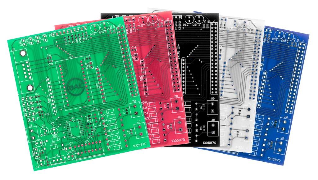
When looking for a reliable PCB manufacturer in Denmark, it’s crucial to partner with a provider that understands local industry needs and global quality standards. The demand for high-precision Denmark PCB products continues to grow, driving the need for professional Denmark PCB manufacturing services that combine technical expertise with efficient delivery. A qualified PCB manufacturer in Denmark should not only master core processes like prototyping, design, and assembly but also comply with strict European regulations such as REACH and RoHS. This guide aims to address common challenges in the Denmark PCB sector, provide practical solutions, and help you make informed decisions when selecting a Denmark PCB manufacturing company.
Are You Facing These Challenges in Denmark PCB Manufacturing?
- Do you struggle with long lead times for PCB prototyping that delay your project progress when cooperating with local Denmark PCB factory?
- Is the high cost of small-batch PCB manufacturing a major burden for your project budget in Denmark?
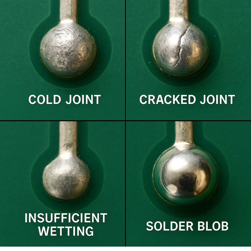
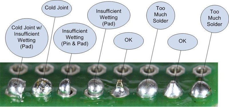
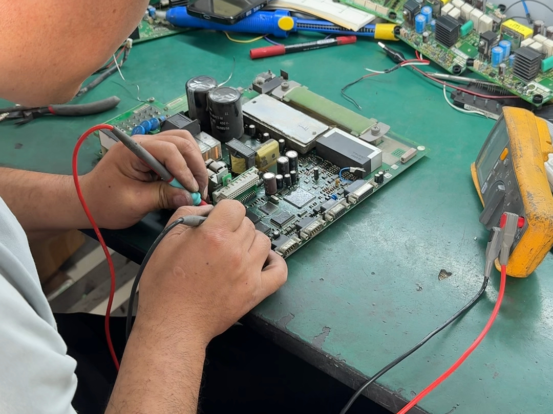
- Have you encountered quality issues such as poor solder joint reliability or inconsistent board thickness from Denmark PCB plant?
- Does the lack of professional design feedback lead to repeated modifications and additional costs during PCB Denmark design and production?
- Are you worried about the compliance of PCB products with EU regulations like REACH and RoHS when working with some Denmark PCB manufacturer?
- Do you often face difficulties in urgent order fulfillment due to inflexible production scheduling of local Denmark PCB company?
End-to-End Assurance from Requirement to Delivery
- Rapid Prototyping: 24-hour fast prototyping delivery with 99.5% yield rate, solving long lead time issues and accelerating your project progress
- Cost-Optimized Solutions: Adopt “small-batch quick return” mode, reducing small-batch production costs by 15-20% through intelligent material matching and process optimization, without compromising product quality.
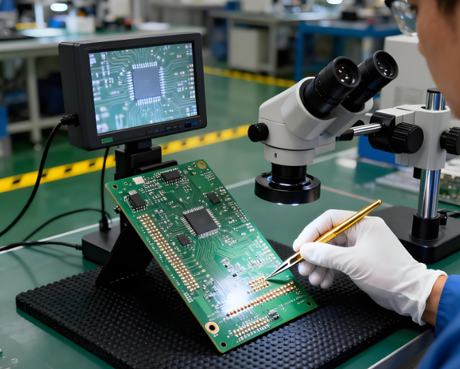
- Strict Quality Control: 100% full inspection for mass production with advanced AOI equipment, achieving 99.9% inspection coverage and 98%+ defect interception rate, ensuring consistent board thickness and reliable solder joints.
- Free DFM Support: Professional free DFM analysis identifies 80%+ potential design flaws in advance, reducing repeated modifications by 70% and shortening the R&D cycle while cutting additional costs.
- Full Compliance Assurance: Strictly comply with EU REACH, RoHS, ISO9001:2015 and ISO13485:2016 standards, with 100% compliance testing for each batch, ensuring Denmark PCB products meet all regulatory requirements.
- Flexible Urgent Order Handling: 2-hour response to urgent orders with a flexible scheduling system, matching our 99.2% on-time delivery rate to fully meet your unexpected production needs.
Why Choose EBest Circuit(Best Technology) as Your PCB Manufacturer in Denmark?
- 19 Years of Industry Expertise: Deep insights into Denmark PCB manufacturing pain points. Our optimized solutions have helped clients reduce comprehensive costs by over 30% cumulatively.
- Free Professional DFM Analysis: Pre-production DFM review identifies 80%+ design flaws in advance, slashing 70% of modification cycles and additional costs.
- Authoritative Compliance Certifications: Hold ISO9001:2015, ISO13485:2016, REACH, RoHS & IATF16949. 100% meets EU regulatory requirements, removing market access barriers.
- Competitive & Transparent Pricing: Local market-oriented cost strategy, combined with intelligent process optimization, cuts your PCB Denmark project costs by 15-20% without compromising quality. No hidden fees, making budget control predictable.
- 24-Hour Fast Prototyping: Urgent orders fulfilled in 24 hours with 99.5% yield rate. Accelerate your product launch cycle and seize market opportunities ahead of competitors.
- 99.2% On-Time Delivery: Rock-solid delivery commitment ensures your production line runs smoothly, avoiding costly downtime caused by delayed supplies.
- Premium Quality Guarantee: 100% full inspection for mass production, with 99.9% inspection coverage and 98%+ defect interception via AOI & X-Ray testing. Consistent quality for every batch.
Top PCB Manufacturer in Denmark List in 2026
| Company Name | Main Business | Core Advantages | Process Capability & Lead Time |
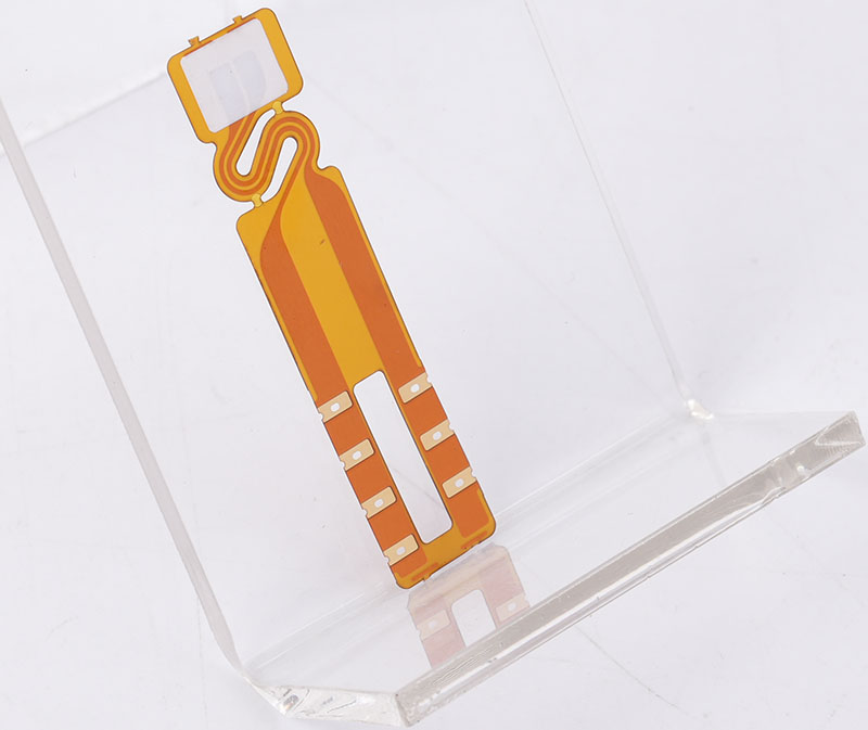
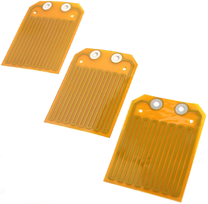
| EBest Circuit Co., Limited (Best Technology Circuit Co., Limited ) | Full series of 1-10 layer rigid, flexible, rigid-flex, RF, heavy copper, metal base, and ceramic PCB processing and assembly | Full-process one-stop service (including IATF 16949/ISO13485 certification) and 46-layer ceramic PCB production capability | Sample delivery in 5-7 days, flexible lead time for small batches; supports high-precision microvias and high-frequency materials |
| NCAB Group Denmark A/S | Multilayer rigid, flexible, rigid-flex, and HDI boards | Green manufacturing system, total cost and delivery accuracy control, extremely fast prototyping service | Standard sample delivery in over 2 days, supports 1-32 layer boards; mass production lead time 6-8 days |
| Møn Print A/S | High-value PCB manufacturing for medical, telecommunications, industrial, and commercial sectors | 50 years of production history, 13 full-industry-chain factories, serving approximately 200 customers | Supports special processes such as FR4, high-frequency materials, and metal substrates; lead time confirmed based on order size |
| GHDsign ApS | PCB design services and production | Established in 1980, a veteran enterprise focused on the “First Time Right” design philosophy | Industry standard lead time of 5-7 days; expert in complex high-end PCB design |
| Azitech ApS | Customized 1-76 layer PCBs, metal substrates, and ceramic boards | European-Asian supply chain network, strict quality control, design support and training | Sample delivery in 5-7 days, mass production in 6-8 days; supports high-reliability requirements |
| PRINTCA AS | High-reliability specialty PCBs for aerospace and defense | ESA (European Space Agency) approved supplier, military and aerospace certified | Lead time meets industry standards, with a focus on high-reliability verification cycles |
| Print Production A/S (formerly manufacturing plant) | PCB trading (formerly a manufacturing plant) | 40 years of history, annual turnover of 12 million Swedish kronor | Lead time dependent on Chinese suppliers, meets industry standards |
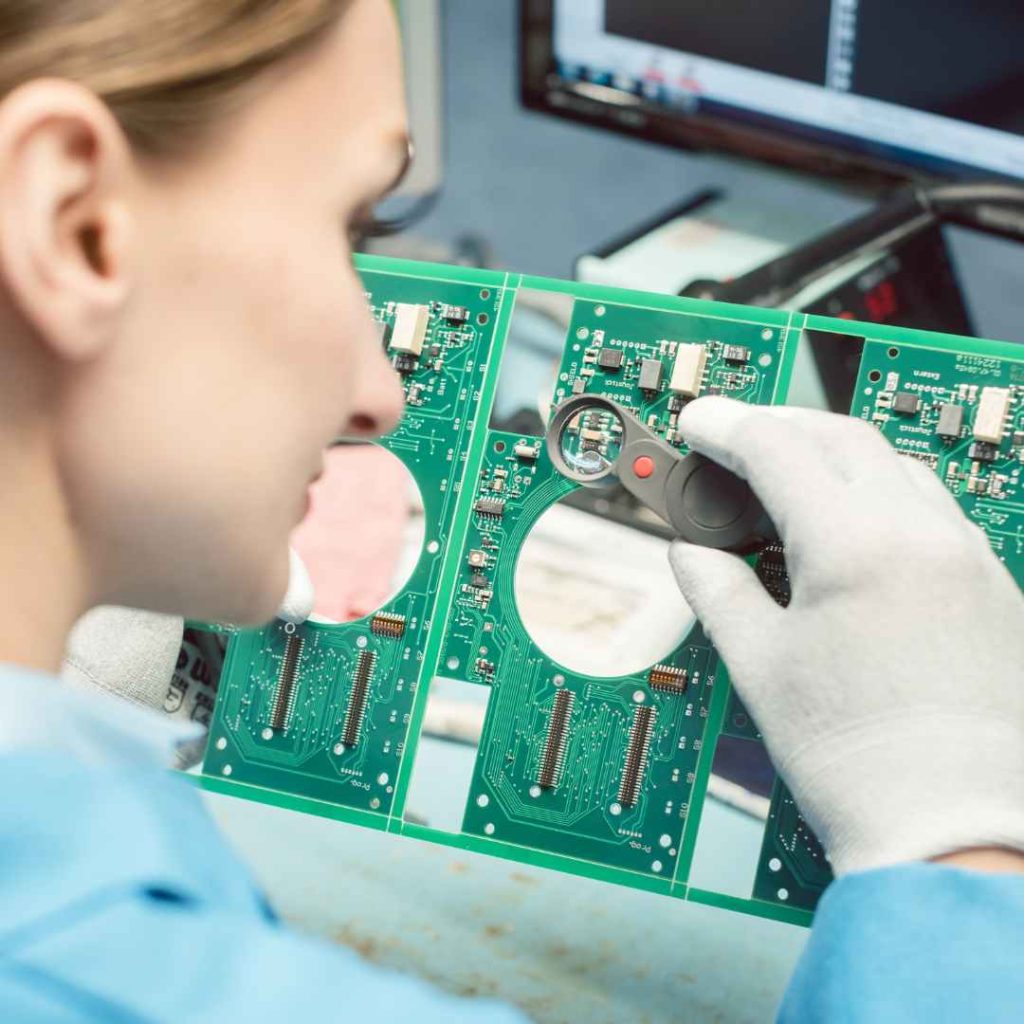
How to Inspect the Quality Management System of PCB Manufacturer in Denmark?
Inspection Guide to Quality Management System of PCB Manufacturer in Denmark:
Verify ISO 9001 Certification and Industry Standards Compliance
- Confirm the manufacturer holds valid ISO 9001 certification and adheres to PCB-specific standards like IPC-A-600/610. Audit documentation for alignment with Denmark’s regulatory requirements (e.g., DS/EN ISO 9001) to ensure baseline quality management practices.
Review Process Control Documentation
- Examine workflow charts, SOPs, and quality control points across production stages (e.g., etching, soldering, testing). Check for real-time monitoring systems (e.g., SPC software) and traceability records to identify deviations or non-conformances.
Audit Supplier and Material Quality Protocols
- Evaluate supplier qualification criteria, incoming material inspection procedures (e.g., AOI for raw PCBs), and COAs (Certificates of Analysis). Assess supplier performance metrics and corrective actions for substandard components.
Inspect Inspection and Testing Procedures
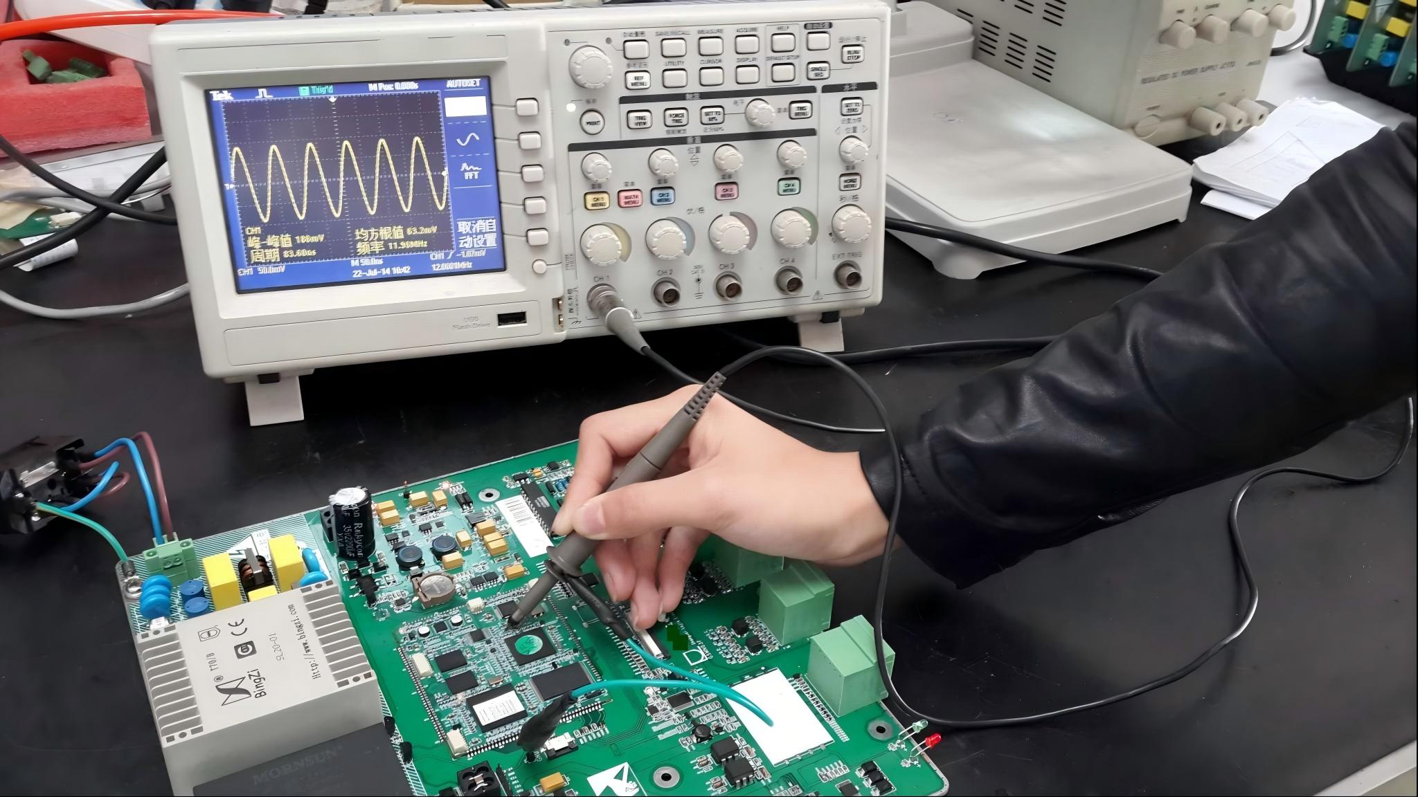
- Validate in-process checks (e.g., visual inspection, electrical testing), final product testing (e.g., X-ray, functional testing), and calibration records for test equipment. Ensure sampling plans meet statistical reliability standards.
Assess Continuous Improvement Mechanisms
- Review internal audit reports, CAPA (Corrective and Preventive Action) logs, and management reviews. Evaluate how customer complaints, field failures, and process audits drive iterative improvements (e.g., PDCA cycles).
Evaluate Employee Training and Competency
- Check training matrices for critical roles (e.g., operators, QA personnel), certifications (e.g., IPC certification), and skill-assessment records. Ensure training programs cover new technologies, safety protocols, and quality awareness.
Examine Environmental and Sustainability Practices
- Verify compliance with EU environmental regulations (e.g., RoHS, REACH) and Denmark’s green manufacturing policies. Audit waste management, energy efficiency, and eco-friendly material sourcing practices.
Analyze Customer Feedback and Complaint Handling
- Review complaint logs, response timelines, and resolution effectiveness. Assess mechanisms for gathering customer feedback (e.g., surveys, NPS scores) and integrating insights into quality upgrades.
How to Evaluate the Process Capability of PCB Manufacturer in Denmark?
Evaluation Guide to Process Capability of PCB Manufacturer in Denmark:
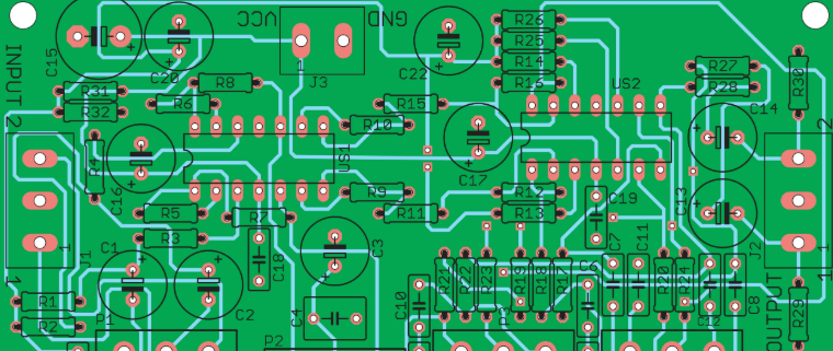
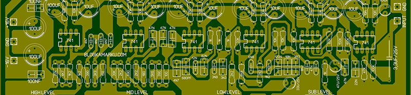
- Verify PCB layer production range and layer alignment precision: Confirm basic capability covers 2-24 layers for general applications; for high-layer demands (16+ layers, common in automotive/industrial control), check if layer-to-layer tolerance can reach ≤ 100μm (critical for signal integrity). Request sample test reports or past project cases for verification.
- Evaluate minimum line width/line spacing precision: This directly determines design density support. For standard PCBs, require ≥ 0.1mm (100μm) capability; for high-precision designs (e.g., IoT/medical devices), confirm if ≤ 0.075mm (75μm) is achievable. Verify via AOI test data and sample micrographs.
- Assess special process capability: For impedance-controlled PCBs, confirm tolerance ±8%~±10% (key for high-frequency signal transmission); for blind/buried vias, check minimum diameter (≤ 0.1mm ideal) and hole location accuracy (±3mil). For high-frequency designs, verify support for materials like Rogers and signal fidelity testing (≥ 99% signal transmission).
- Inspect production equipment advancement: High-speed SMT should have placement accuracy ±0.03mm to support 01005/0.3mm pitch BGA; multi-zone reflow ovens ensure uniform soldering; AOI equipment needs ≥ 99.9% defect coverage (combining pre- and post-furnace testing) to reduce hidden quality issues.
- Evaluate technical team proficiency: Prioritize teams with 5+ years of process engineering experience; confirm operators hold IPC-A-610 certification (electronic assembly standard). Discuss design challenges (e.g., thermal management for industrial PCBs) to assess their problem-solving ability.
- Review key process verification documents: IQ/OQ/PQ reports for drilling, plating, and soldering processes must include parameter fluctuation data (≤ ±5%) and process capability index (CPK ≥ 1.33) to ensure stable production repeatability.
- Check production capacity and scalability: Confirm monthly capacity (e.g., 5,000-50,000㎡) matches your order scale. For project growth needs, verify if 2x capacity expansion within 30 days is feasible, avoiding supply chain disruptions during batch scaling.
How to Evaluate the Delivery Reliability of Denmark PCB Manufacturing Company?
Evaluation Guide to Delivery Reliability of Denmark PCB Manufacturing Company:
- Verify the manufacturer’s historical On-Time Delivery (OTD) rate: request at least 6 months of delivery statistics (not just customer feedback) to confirm a consistent OTD rate of ≥95%, a benchmark for reliable PCB suppliers in the industry.
- Assess the flexibility of their production scheduling system (e.g., MES system integration): Confirm it can handle urgent prototype orders (24–48 hour response) and adapt to last-minute design changes without significant delivery delays.
- Evaluate supply chain stability: Check if they have qualified alternative suppliers for key raw materials (e.g., high-frequency substrates) and a documented contingency plan for supply chain disruptions (e.g., geopolitical issues, logistics crises).
- Review logistics and transportation capabilities: Confirm they partner with reputable logistics providers experienced in electronic components shipping, with solutions for special requirements (e.g., anti-static packaging, temperature control) and backup plans for extreme weather or customs delays.
- Clarify delivery progress communication protocols: Ensure they offer real-time tracking (via project management platforms or CRM) and proactive alerts, ideally 48 hours in advance—for potential delays that could impact your project timeline.
- Investigate post-delivery support for delays: Confirm they have a formal SLA (Service Level Agreement) outlining compensation (e.g., late delivery penalties) and corrective actions (e.g., 8D reports) to prevent recurrence.
- Validate key raw material inventory management: Check if they maintain safety stock for critical materials (e.g., FR-4, copper clad laminates) and have inventory alert systems to avoid production halts due to material shortages.

FAQs of Denmark PCB Manufacturing
Q1: How to address design-related high production scrap rates?
A1: Free pre-production DFM analysis identifies issues like improper pad design, insufficient copper spacing, and mismatched hole sizes, reducing scrap rates and production costs effectively.
Q2: Is fast delivery available for urgent prototypes without quality compromise?
A2: 24-hour urgent prototyping is available. All prototypes undergo AOI and circuit continuity testing, ensuring quality while meeting tight deadlines.
Q3: How to ensure EU REACH and RoHS compliance?
A3: We use certified raw material suppliers, conduct batch testing, hold REACH/RoHS certifications, and provide full compliance reports to meet EU regulations.
Q4: Are there cost-effective solutions for small-batch production?
A4: Yes. We optimize costs via batch combination and material selection, with transparent pricing (no hidden fees) for small-batch PCB Denmark manufacturing.
Q5: What if delivered PCBs have quality issues?
A5: Contact us with test reports/samples; we conduct a full analysis within 24 hours. Production-caused issues will be resolved via re-production, replacement, or refund per agreement.