PCB manufacturing PCB manufacturing
Home > Blog

Posts Tagged ‘surface mount technology’

What Is an SMT PCB Board? SMT PCB Assembly
Thursday, January 8th, 2026

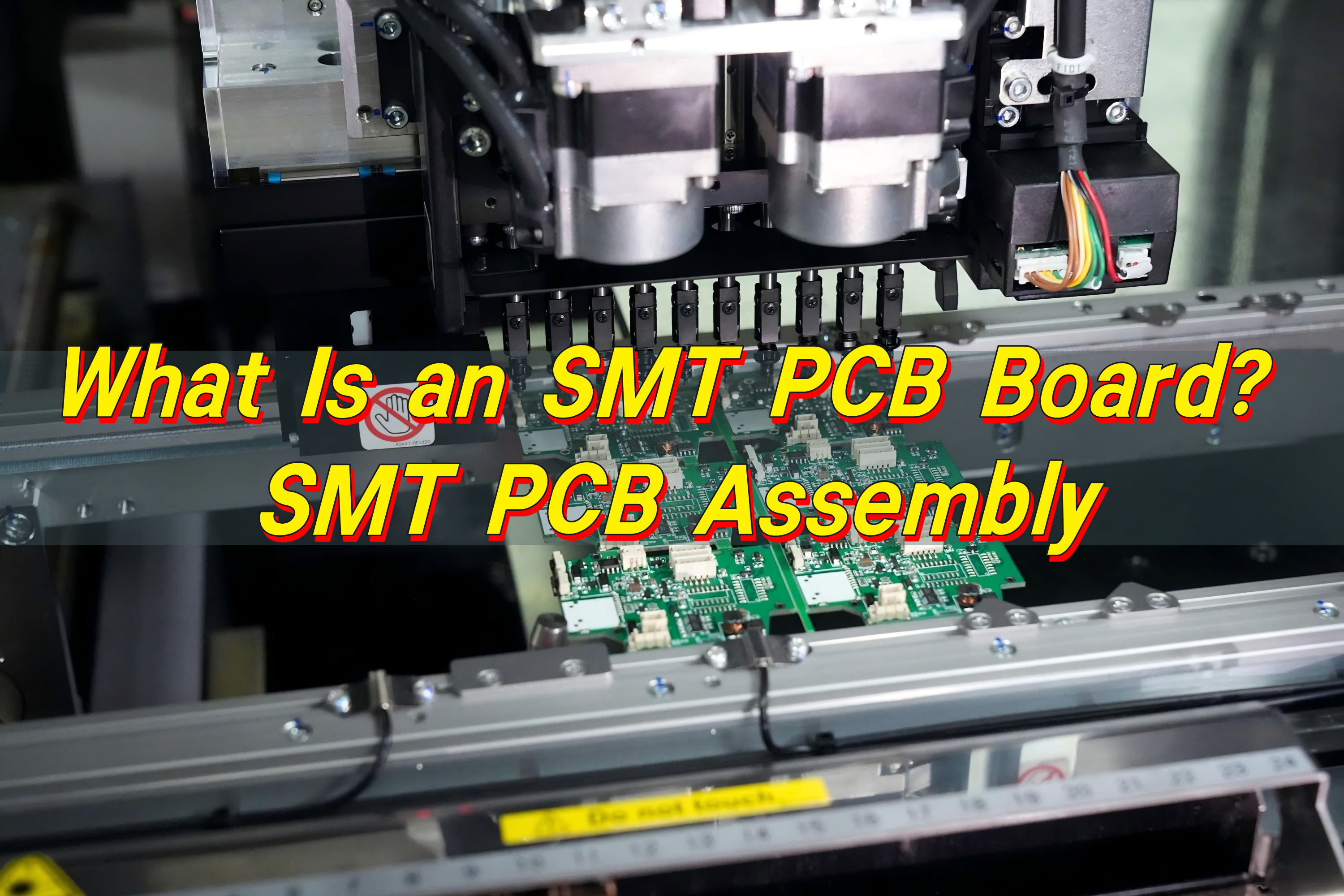
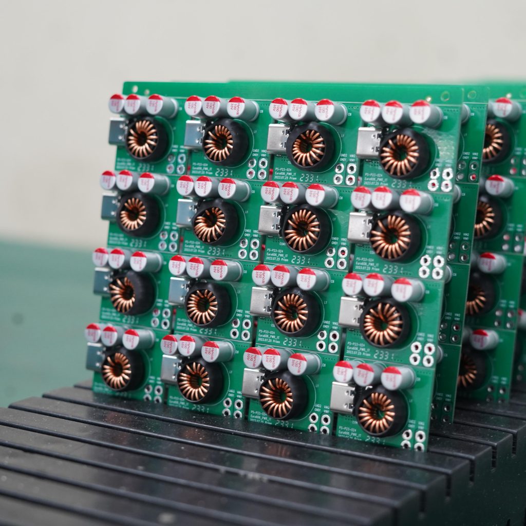
An SMT PCB board is a printed circuit board designed for surface mount technology, where electronic components are mounted directly onto copper pads on the board surface rather than inserted through drilled holes. This approach allows components to sit flat against the PCB, enabling compact layouts, shorter electrical paths, and efficient automated assembly through reflow soldering. As a result, SMT PCB boards support higher component density while maintaining consistent solder quality.

What Is an SMT PCB Board? SMT PCB Assembly

What Is an SMT PCB?

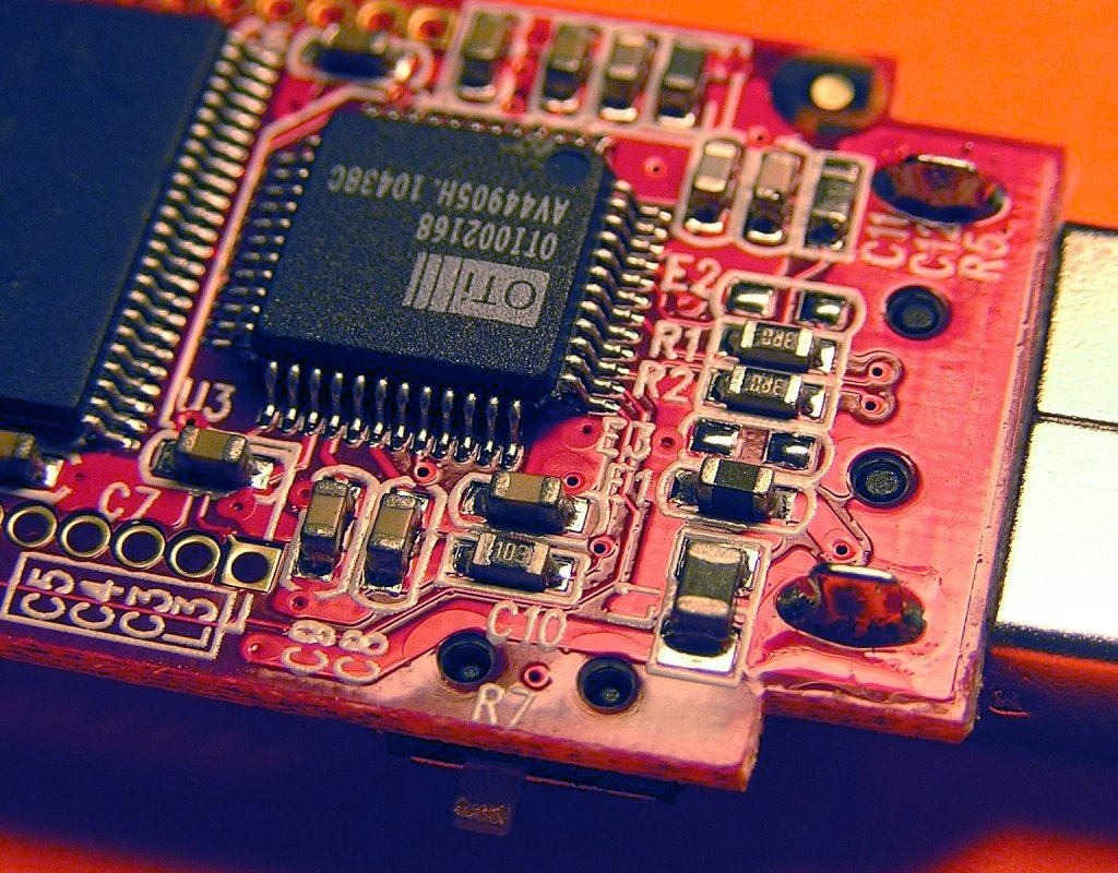
An SMT PCB is a printed circuit board designed specifically for surface mount technology, where electronic components are mounted directly onto copper pads on the surface of the board. Unlike traditional assembly methods, components do not use long wire leads inserted through drilled holes. Instead, they sit flat against the PCB and are soldered in place using controlled reflow processes.

This structural change enables much higher component density. Components can be placed on both sides of the board, and spacing between parts can be significantly reduced. As a result, SMT PCB boards are smaller, lighter, and more electrically efficient than older designs.

Another key benefit is manufacturing consistency. SMT placement is highly automated, allowing machines to position thousands of components per hour with exceptional accuracy. This repeatability improves yield and reduces defect rates, especially in high-volume production.

SMT PCB boards are now standard across consumer electronics, medical equipment, industrial controls, automotive electronics, and communication systems.

How Does SMT Impact PCB Design?

SMT influences PCB design from the earliest layout stage. Because surface-mounted components have short electrical paths, signal integrity improves, especially in high-speed and high-frequency circuits. This allows designers greater flexibility when routing traces and managing impedance.

Pad design becomes a critical factor in SMT layouts. Pad size, shape, and spacing directly affect solder joint quality and long-term reliability. Improper pad geometry can lead to solder bridging, tombstoning, or weak joints, all of which increase rework risk.

Layer stack-up also changes with SMT. Multilayer boards are common, as designers use internal planes for power distribution and noise control. Thermal management becomes more important as well, since compact components can generate localized heat that must be dissipated efficiently.

Finally, SMT PCB design must align with assembly equipment capability. Package size limits, placement tolerances, and inspection access all influence layout decisions.

Is SMT the Same as SMD?

SMT and SMD are closely related terms, but they are not interchangeable. SMT stands for surface mount technology and refers to the manufacturing process used to assemble components onto a PCB. SMD stands for surface mount device and refers to the component itself.

In simple terms, SMT is the method, while SMD is the part. Factories use SMT processes to place SMD components onto SMT PCB boards.

What Is an SMT PCB Board? SMT PCB Assembly

What Is the Difference Between SMD and SMT PCB?

An SMT PCB describes both the board design and the assembly method, while an SMD describes only the component package. SMT PCBs are designed with specific land patterns that support surface-mounted components and reflow soldering processes.

SMD components include chip resistors, capacitors, integrated circuits, and discrete semiconductors packaged for surface mounting. Without an SMT-compatible PCB, SMD components cannot be properly assembled or soldered.

In practice, SMT PCBs and SMD components always work together, but their roles are distinct.

How Does PCB Board SMT Differ From Through-Hole Assembly?

The difference between SMT and through-hole assembly is structural and operational. Through-hole assembly uses drilled holes where component leads pass through the board and are soldered on the opposite side. SMT places components directly onto surface pads without penetrating the board.

SMT enables much higher component density and allows assembly on both sides of the PCB. This supports smaller board sizes and more complex functionality. Through-hole assembly, while mechanically robust, occupies more space and limits layout flexibility.

SMT also supports full automation, while through-hole assembly often requires manual or semi-automated steps. This difference has a significant impact on cost and scalability. However, some products use both methods together, such as board assembly SMT DIP PCB or board assembly SMT THT PCB designs, where connectors or power components still benefit from through-hole strength.

What Is the Major Advantage of Using SMT?

The primary advantage of SMT PCB assembly is efficiency at scale. Automated placement machines operate at high speed with consistent accuracy, enabling reliable mass production. This efficiency directly reduces assembly time and labor costs.

SMT also supports miniaturization. More functionality fits into less space, enabling thinner, lighter, and more portable devices. Electrical performance improves as well, since shorter lead lengths reduce parasitic effects and signal noise.

Reliability benefits from controlled soldering processes. Reflow soldering produces uniform joints, reducing variation and long-term failure risk.

What Components Are Used in SMT?

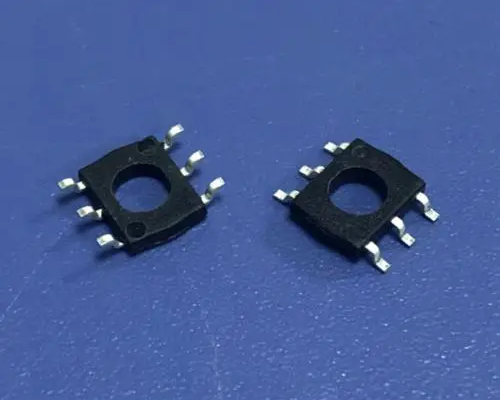
SMT supports a wide range of electronic components. Common passive parts include chip resistors and capacitors in standardized package sizes. Integrated circuits appear in formats such as SOIC, QFP, QFN, and BGA, supporting everything from simple logic to advanced processors.

Discrete components like diodes, transistors, and MOSFETs are widely used in SMT designs. Many connectors and RF modules are also available in surface-mount packages, allowing compact system integration.

Each component type requires proper footprint design, accurate stencil thickness, and precise placement to ensure reliable solder joints. Successful SMT PCB assembly depends on matching component selection with process capability.

What Quality Checks Are Used in SMT PCB Assembly?

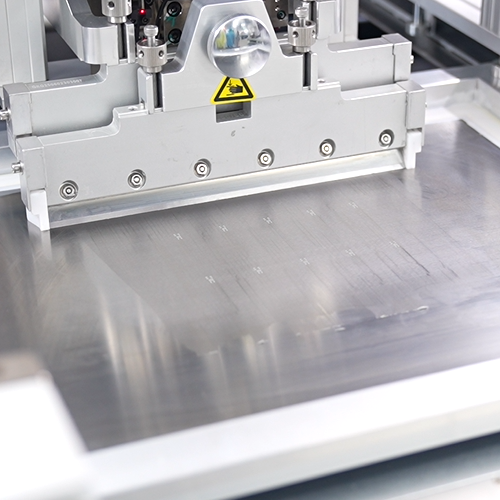
Quality control is central to SMT PCB assembly. Inspection begins with solder paste application, where volume and alignment are monitored to prevent downstream defects. Automated optical inspection then verifies component placement and visible solder joints.

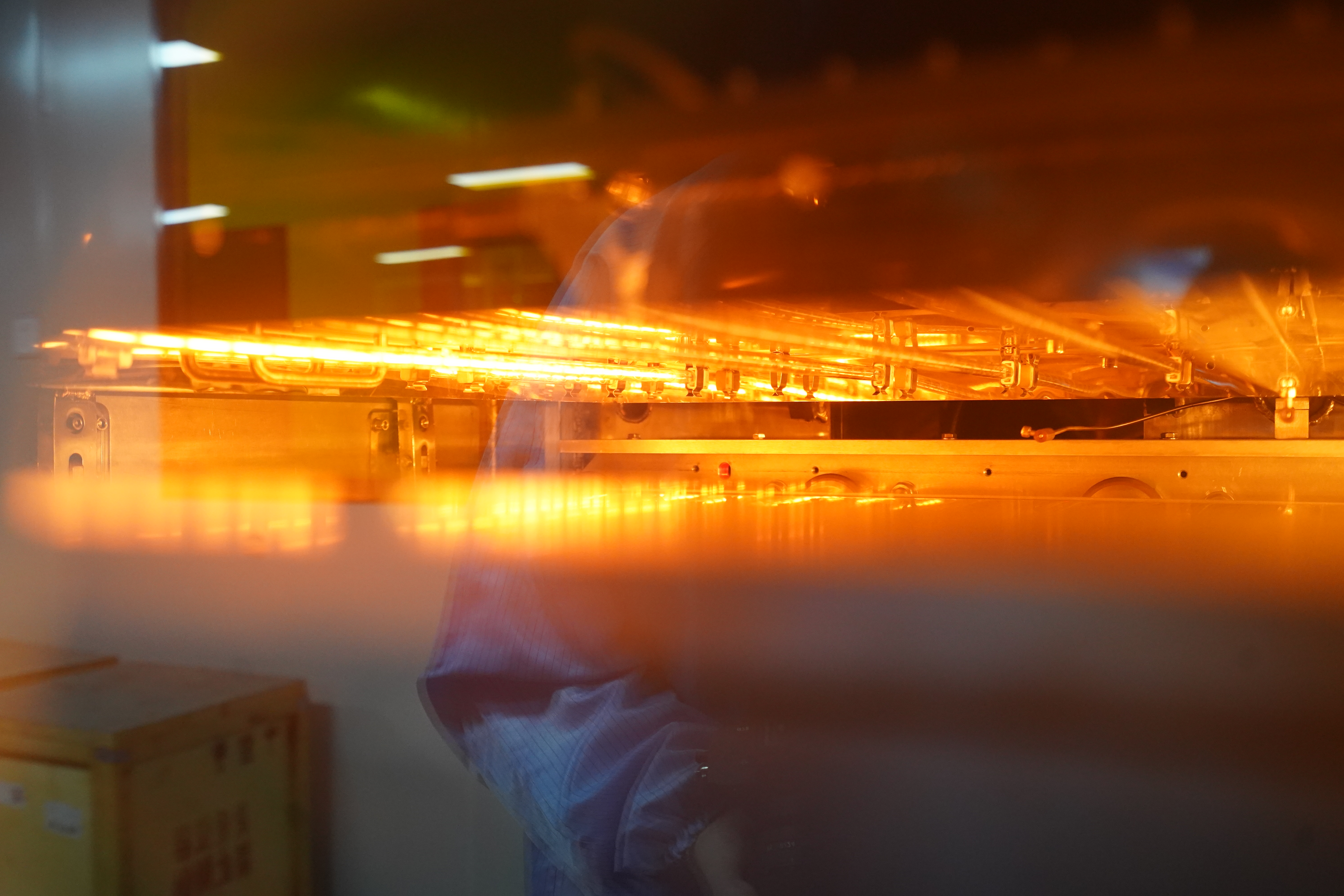
For components with hidden connections, such as BGAs, X-ray inspection is used to evaluate internal solder quality. Reflow temperature profiles are carefully controlled to avoid thermal damage or weak joints.

Electrical testing confirms circuit continuity and functionality, while final inspection ensures cleanliness and cosmetic quality. These layered quality checks protect product reliability and customer confidence.

What Is an SMT PCB Board? SMT PCB Assembly

Where Do We Use SMT?

SMT is used across nearly every electronics sector. Consumer electronics rely on it for compact form factors and high functionality. Industrial and medical devices depend on SMT for precision, consistency, and long-term reliability.

Automotive electronics use SMT for control units and sensor systems that must withstand harsh conditions. Telecommunications and networking equipment rely on SMT to support high-speed signal performance and dense layouts.

As electronics continue to evolve, SMT PCB assembly remains a foundational technology enabling innovation at scale.

Conclusion:

An SMT PCB board is a circuit board built for surface mount technology, where components are placed on surface pads and soldered by reflow for fast, repeatable production. Compared with through-hole assembly, SMT PCB assembly supports higher density, smaller products, and strong electrical performance, which is why it dominates modern electronics.

To learn more about how Best Technology supports these SMT PCB assembly technologies, please contact us at sales@bestpcbs.com

What is the surface mount technology?
Friday, August 23rd, 2024

Surface mount technology (SMT) is a widely used surface assembly method in the electronic assembly industry. It mainly uses automated production equipment to directly solder surface mount components (SMD) to the pads on the surface of the printed circuit board (PCB). SMT has the advantages of high production efficiency, high space utilization, high density and miniaturization. However, it has high requirements for production equipment, processes and operating skills.

What is the surface mount technology process?

The process of surface mount technology (SMT) mainly includes the following steps:

1. Printed circuit board preparation: Before surface mounting, the printed circuit board needs to be prepared first, including cleaning the circuit board, removing the surface oxide layer, and applying solder paste.

What is the surface mount technology ?

2. Component mounting: Use appropriate equipment to accurately mount various electronic components on the printed circuit board.

3. Soldering: After the components are mounted, the solder paste is heated to melt it to form a reliable welding connection.

4. Inspection: After welding, use AOI for automatic inspection to ensure the correct mounting and welding quality of components.

5. Testing and debugging: Test and debug the mounted circuit board, and verify whether the function and performance of the circuit board meet the requirements through specific test equipment and procedures.

Each step needs to be carried out carefully to ensure that the mounted circuit board has good quality and reliability. In addition, surface mount technology is suitable for circuit board assembly, with the characteristics of compact structure and small size, and is widely used in the manufacture of electronic products.

What are the roles of surface mount?

The role of surface mount technology (SMT) is mainly reflected in improving the performance, reliability and production efficiency of electronic products, while reducing the volume and weight of products.

Surface mount technology (SMT) has the following significant effects:

Increase assembly density and reduce product volume: By using surface mount technology, the volume of electronic products can be reduced by 40%~60% and the weight can be reduced by 60%~80%.

What is the surface mount technology ?

‌Improve reliability: SMT has high reliability, low solder joint defect rate and strong vibration resistance.

Optimize high-frequency characteristics: SMT reduces electromagnetic and radio frequency interference and optimizes the high-frequency characteristics of the circuit.

Automated production: SMT is easy to automate, thereby improving production efficiency.

Enhanced compactness: Using small surface-mounted components can save a lot of space on the printed circuit board, and circuit assembly is easier to automate.

Adapt to a wide range of fields: As a new generation of electronic assembly technology, SMT has penetrated into various fields, including but not limited to computers, communication equipment, consumer electronics, etc.

In summary, surface mounting technology has significantly improved the comprehensive performance and production efficiency of modern electronic products by increasing assembly density, optimizing circuit performance, enhancing product reliability, and realizing automated production.

What is the advantage of surface mount?

The advantages of surface mounting mainly include:

High assembly density: Surface mounting technology (SMT) allows more electronic components to be installed in a limited space.

Small size and light weight of electronic products: By using SMT, smaller and lighter electronic products can be manufactured.

‌High reliability‌: SMT has a low solder joint defect rate, which improves the reliability of the product‌.

‌Easy to automate‌: SMT technology is very suitable for automated production and can greatly improve production efficiency‌.

‌Design flexibility‌: SMT allows different components to be used on the same circuit board, providing design flexibility‌.

‌EMC compliance‌: SMT technology helps meet electromagnetic compatibility (EMC) requirements and ensure the safety and performance of the equipment‌.

‌Selective soldering‌: SMT supports selective soldering, which increases the customizability of the product‌.

In addition, SMT technology is cost-effective because the packaging size of components is generally standardized and can be quickly and accurately installed using automated equipment, thereby reducing production costs‌. At the same time, SMT reduces human errors and improves product quality because the placement of components is very consistent, reducing errors or the need for rework.

What are the disadvantages of surface mount?

‌The disadvantages of surface mount technology (SMT) mainly include incompatibility with certain components, the possibility of soldering defects, and high equipment costs. ‌

‌Incompatibility with certain components‌: SMT technology is not suitable for all types of components.

‌Possibility of soldering defects‌: Although SMT technology reduces the need for drilling and shortens setup time, it is not a zero-defect soldering process. In actual applications, SMT may encounter various soldering defects.

‌Higher equipment cost‌: Although SMT technology can improve production efficiency and circuit density, it requires expensive special equipment and professional technicians.

In summary, although SMT technology has many advantages, such as reducing drilling, shortening setup time, and improving production efficiency, it also has some disadvantages, especially in terms of incompatibility with certain components, possible soldering defects, and high equipment costs.

What does SMD stand for in surface mount?

SMD stands for Surface Mounted Devices. ‌

SMD is a type of component in surface mount technology (SMT), which is characterized by small size, high power, stable performance, and easy automated assembly.

What is the surface mount technology ?

SMD packaging technology can maximize the space utilization on the circuit board, especially for the design of dense circuit boards. SMD packaging usually adopts metal oxide semiconductor (MOS) technology, and its packaging methods are diverse, including COB, QFN, LCC, BGA, etc.

In practical applications, the appearance inspection of SMD devices includes visual inspection or use of a magnifying glass to check whether the solder end or pin surface is oxidized or has contaminants, and to ensure that the nominal value, specification, model, accuracy, and external dimensions of the components are consistent with the product process requirements. To ensure the performance and reliability of the device.

The wide application of SMD technology not only improves the performance of electronic products, but also promotes the automation and efficiency improvement of the electronics manufacturing industry. It is an indispensable part of the modern electronics manufacturing industry, especially in applications that require high integration and high reliability.

What is the application of surface mount?

The application of surface mount technology is mainly reflected in improving production efficiency, reducing product volume and weight, and meeting the market demand for miniaturized, lightweight, and high-performance electronic products. This technology is mainly used to mount electronic components on printed circuit boards (PCBs) to achieve circuit connection and system integration.

Surface mount technology can replace traditional through-hole insertion technology, thereby improving product reliability and performance and reducing costs. The technology has a wide range of applications, including but not limited to consumer electronics, military cutting-edge electronics, and fire detectors, manual alarms, and various electronic modules.

In the manufacture of electronic products, surface mount technology has become a revolutionary change, dominating the development of electronic equipment and bringing about major changes in electronic products.

Conclusion:

Usually, the electronic products we use are designed by PCB plus various capacitors, resistors and other electronic components according to the designed circuit diagram, so most electrical appliances require various SMT (patch) processing technologies to process.

BEST Technology focuses on the procurement and processing of various electronic products and processing services for incoming materials, including but not limited to SMT patches, DIP plug-ins, welding, functional testing and maintenance, and assembly proofing and batch production. We can provide proofing, small batch and batch SMT mounting, and can also purchase electronic components and make PCBs.