

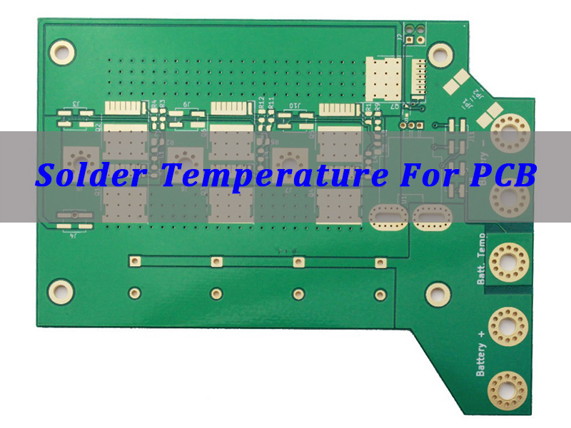
Solder temperature for PCB is the precise thermal profile applied to melt solder and form reliable electrical and mechanical connections between components and the board, and its control is the single most critical factor in assembly quality. This definitive guide explores the science, standards, and practical controls behind achieving the perfect solder temperature for PCB in both manual and automated processes.
What are the most frustrating challenges engineers and assemblers face when dealing with PCB solder temperature?
- Inconsistent joint quality and reliability due to vague or undocumented temperature settings.
- Damaging heat-sensitive components (like MLCCs or connectors) during hand soldering or rework.
- Experiencing soldering defects like cold joints, bridging, or tombstoning without knowing the root cause.
- Struggling to find the right solder iron temperature for PCB rework on mixed-technology boards.
- Failing BGA reliability tests due to an improperly characterized reflow profile.
These proven solutions effectively counteract the challenges at hand.
- Developing and adhering to detailed Process Control Documents (PCDs) for each solder alloy and board type.
- Utilizing thermally profiled soldering stations with closed-loop control and appropriate tip selection for sensitive components.
- Implementing real-time process monitoring and Post-Solder Inspection (AOI, X-ray) to link defects directly to thermal cause.
- Providing technicians with clear guidelines and training on adjusting the solder iron temperature for PCB based on pad size, component mass, and layer count.
- Characterizing the specific PCB solder temperature for BGA reflow through empirical thermal profiling and solder ball analysis.
At EBest Circuit (Best Technology), we recognize that precision in soldering defines reliability. As a professional PCBA manufacturer, we invest in state-of-the-art reflow ovens with real-time profiling, expert process engineering, and stringent IPC-certified standards to ensure every joint on your board—from a 0201 resistor to a complex BGA—is formed under optimal thermal conditions. Pls feel free to contact our team at sales@bestpcbs.com for any PCBA soldering questions.
What Is the Correct Solder Temperature for PCB and How to Control It?
The “correct” solder temperature for PCB is not a single number but a temperature profile tailored to the specific solder alloy, component packaging, PCB mass, and the soldering method used. It is the range that completely melts the solder (exceeding the liquidus temperature) to form a proper intermetallic bond without exceeding the thermal limits of the components or substrate.
Controlling this temperature is a systematic engineering practice, not guesswork. It involves:
- Understanding Materials: Knowing the liquidus temperature of your solder paste (e.g., ~217°C for SAC305) and the maximum temperature ratings of all components.
- Measurement and Profiling: Using data-logging thermocouples to map the actual temperature experienced by the board during the process.
- Process Parameter Adjustment: Fine-tuning machine settings (like conveyor speed, zone temperatures) to match the target profile.
- Continuous Monitoring: Using oven sensors and periodic re-profiling to ensure the process remains in control over time.
In essence, the correct temperature is a verified profile that ensures complete solder fusion and reliable intermetallic formation while staying within the safe thermal window of the entire assembly.
What Is the Recommended Solder Temperature for PCB During Assembly?
In automated SMT manufacturing, the solder temperature for PCB is controlled through a thermal profile rather than a single temperature value.
This profile is usually defined by a time-temperature curve inside the reflow oven. Each stage gradually heats the PCB, melts the solder paste, and then cools the joint to form a strong metallurgical bond.
For the commonly used lead-free SAC305 solder alloy, a typical reflow profile looks like the following.
| Profile Stage | Target Temperature |
|---|---|
| Preheat / Ramp | 1–3°C/sec to 150–180°C |
| Soak | 150–200°C for 60–120 sec |
| Reflow / Liquidus | Above 217°C for 45–90 sec |
| Peak Temperature | 240–250°C |
| Cooling | −1 to −4°C/sec |
These parameters help the PCB assembly process reach stable solder joints without damaging components.
Preheat Stage
The preheat stage slowly increases the board temperature.
This step removes solvents from the solder paste and prevents thermal shock to sensitive components.
Soak Stage
During the soak stage, the PCB temperature stabilizes between 150°C and 200°C.
This allows the entire board, including large copper areas and dense components, to reach a uniform temperature.
Reflow Stage
When the temperature rises above 217°C, the SAC305 solder alloy becomes liquid.
At this moment, the molten solder wets the pads and component leads to form reliable electrical connections.
Peak Temperature
The peak temperature is usually 240–250°C for lead-free soldering.
This level ensures complete solder melting while staying below the maximum thermal limit of most electronic components.
Cooling Stage
Controlled cooling solidifies the solder joints.
A proper cooling rate helps create a fine and strong grain structure inside the solder.
Critical Note:
These values are general references. The exact solder temperature for PCB assembly must follow the solder paste datasheet and the thermal limits of the most sensitive component on the board.
In professional manufacturing, engineers always perform a reflow thermal profiling test to verify the correct process settings before mass production.
How to Choose the Right Solder Iron Temperature for PCB Manual Soldering?
Selecting the right solder iron temperature for PCB manual rework or repair is a balance between providing enough heat to form a good joint quickly and minimizing thermal stress. A fixed, universal setting is a common pitfall.
Follow this decision framework:
- Start with the Solder Alloy: Set the baseline above the solder’s liquidus temperature. For Sn63Pb37 (melts at ~183°C), start at 315-345°C. For lead-free SAC305, start at 345-375°C.
- Factor in Thermal Mass: Increase temperature for larger components, ground planes, or multi-layer boards that sink heat. A small SMT resistor may need 320°C, while a multi-pin connector on a thick board may require 380°C or more.
- Consider Component Sensitivity: Decrease temperature for heat-sensitive parts (e.g., LEDs, plastic connectors). Use the minimum effective temperature.
- Use the Right Tip: A larger, chisel tip transfers heat more efficiently than a fine conical tip, allowing you to use a lowerset temperature for the same joint.
- Technique is Key: Apply the iron tip to the pad and lead simultaneously to heat both, then feed solder. The joint should form within 2-3 seconds. If it takes longer, increase temperature slightly; if the flux smokes violently or the PCB discolors, decrease it.
The goal is to melt the solder and flow it into the joint quickly, minimizing the duration of heat exposure.
What Is the Ideal PCB Solder Temperature for BGA Reflow Process?
The ideal PCB solder temperature for BGA reflow demands greater precision than for typical SMT components due to hidden joints and thermal mass. The primary goal is to ensure all solder balls under the package reliably melt and collapse, forming a proper connection without causing voids or damaging the die.
Key profile considerations for BGA reflow:
- Higher Peak Temperature: BGAs often require a peak temperature at the top of the package in the range of 245-260°C to ensure the solder balls at the board interface (which can be 5-15°C cooler) still exceed the liquidus point (~217-220°C).
- Adequate Time Above Liquidus (TAL): A longer TAL, typically 60-90 seconds, is crucial to allow all BGA balls to fully reflow and for any gasses to escape, minimizing void formation.
- Ramp-Up Control: A controlled ramp rate (1-2°C/sec) during preheat is vital to prevent solder ball “slumping” or coalescing before reflow.
- Thermal Uniformity: The profile must ensure less than a 5°C difference across the BGA body to prevent warpage and non-uniform collapse.
Therefore, the ideal PCB solder temperature for BGA is part of a carefully profiled curve that emphasizes sufficient, uniform heat delivery to the hidden joint array, validated through cross-sectioning or X-ray analysis to confirm full ball collapse and minimal voids.
Why Does Solder Temperature for PCB Affect Solder Joint Reliability?
The solder temperature for PCB directly dictates the metallurgical quality of the intermetallic compound (IMC) layer formed between the solder and the component termination/pad. This IMC is the actual bonding interface, and its structure determines long-term reliability.
- Too Low (Cold Joint): Temperature fails to fully melt the solder or wet the surfaces. The result is a grainy, weak mechanical bond with high electrical resistance. It fails under thermal cycling or vibration.
- Correct Range: Provides optimal energy for forming a thin, uniform, and durable IMC layer (e.g., Cu6Sn5 for copper pads). This creates a strong, ductile joint that can absorb mechanical and thermal stress.
- Too High or Prolonged: Excessive heat accelerates IMC growth, forming a thick, brittle layer (like Cu3Sn). It also coarsens the solder grain structure. Both factors make the joint prone to cracking under stress. Extreme heat can also delaminate the PCB or damage components.
In summary, precise temperature control ensures the formation of a reliable IMC—too little heat prevents its proper formation, while too much heat corrupts it, with both scenarios leading to premature field failures.
How Does Incorrect Solder Temperature for PCB Cause Common Soldering Defects?
Incorrect solder temperature for PCB is one of the most common reasons for soldering defects.
When the temperature is too low, solder cannot fully melt and wet the pad. When it is too high, the PCB or components may suffer thermal damage.
The table below shows how temperature mistakes quickly translate into common soldering problems.
| Defect | Likely Temperature Cause |
|---|---|
| Cold Solder Joint | Temperature too low |
| Solder Bridging | Excessive or uneven heat |
| Tombstoning | Uneven heating |
| Solder Balls | Heating too fast |
| Wicking | Iron temperature too high |
| Pad / PCB Delamination | Excessive thermal exposure |
| BGA Voids | Incorrect TAL or ramp rate |
Although the causes above look simple, each defect relates to how heat flows through the PCB during soldering. Understanding these mechanisms helps engineers avoid reliability issues in production.
Cold Solder Joint
Cold joints usually appear dull and rough. They occur when the solder never reaches full liquid state.
This often happens when the soldering iron temperature is too low or when the reflow peak temperature is insufficient.
Solder Bridging
Bridging happens when molten solder connects two adjacent pads.
If the reflow temperature is too high or uneven, solder paste can slump and flow between pins. Fine-pitch components are especially sensitive to this issue.
Tombstoning
Tombstoning occurs when one side of a chip component lifts during reflow.
This is often caused by uneven heating between the two pads of the component. When one pad melts earlier, surface tension pulls the component upright.
Solder Balls And Splatter
Solder balls usually form when heating is too rapid during the preheat stage.
The solvent inside solder paste can vaporize quickly and push tiny solder particles away from the pad.
Wicking
Wicking happens mostly during manual soldering.
When the solder iron temperature is too high, molten solder travels up the component lead instead of staying on the pad. This leaves the pad with insufficient solder.
Pad Or PCB Delamination
If the solder temperature for PCB is excessively high for too long, the laminate can weaken.
The PCB resin may soften once it approaches its glass transition temperature (Tg), leading to pad lifting or board delamination.
BGA Voids
BGA voids form when flux gases become trapped inside the solder joint.
Incorrect ramp rates or insufficient time above liquidus (TAL) during reflow often cause this issue.
Controlling the thermal profile is therefore the most important factor in preventing soldering defects. Stable temperature control ensures good wetting, strong solder joints, and reliable PCB assemblies.
What Factors Determine the Proper Solder Temperature for PCB Components?
The proper solder temperature for PCB is a complex result of several interdependent factors. Engineers must balance all of these to define a safe and effective process window.
- Solder Alloy Composition: The fundamental driver. The liquidus temperature sets the minimum (e.g., 183°C for SnPb, 217°C for SAC305, 221°C for SAC305+Bi).
- Component Thermal Mass & Size: A large QFP or BGA requires more heat energy (higher peak/longer TAL) than a 0402 resistor. The largest and smallest components on the board set the profile boundaries.
- Component Thermal Sensitivity: The maximum temperature limit of the most sensitive component (often stated on its datasheet) sets the absolute ceiling for peak temperature.
- PCB Characteristics: Board thickness, layer count, copper density, and internal planes act as a heat sink. A heavy multi-layer board requires a more aggressive profile than a simple 2-layer board.
- PCB Material (Tg): The glass transition temperature of the laminate material must not be exceeded for prolonged periods to prevent delamination or z-axis expansion.
- Surface Finish: Different finishes (ENIG, Immersion Sn, OSP) have varying wettability and may slightly influence ideal temperature.
- Soldering Method: Wave soldering, selective soldering, vapor phase, and laser soldering all have unique temperature dynamics and control mechanisms.
How Do Engineers Control PCB Solder Temperature in SMT and Reflow?
In SMT reflow soldering, controlling the PCB solder temperature is achieved through a closed-loop system of profiling, oven calibration, and monitoring. It is a precise engineering discipline, not a simple thermostat setting.
The Control Process:
- Step 1: Create a Target Profile. Based on the factors above (solder paste datasheet + component limits), engineers define a target time-temperature curve.
- Step 2: Physical Profiling. A profiling board equipped with thermocouples attached to key components (especially the smallest and largest) is run through the oven. Data is recorded.
- Step 3: Oven Setting Adjustment. Engineers adjust the oven’s zone temperatures and conveyor speed to make the actual measured profile match the target profile as closely as possible. This is an iterative process.
- Step 4: Validation & Documentation. The final profile is documented in the Process Control Plan. First-article boards are inspected (via X-ray for BGAs) to validate joint quality.
- Step 5: Ongoing Monitoring. Modern reflow ovens have built-in thermocouples that continuously monitor the profile. Statistical Process Control (SPC) charts track conveyor speed and zone temperatures to detect drift. Periodic re-profiling is done for new boards or as preventive maintenance.
This rigorous approach ensures that every board in the production run experiences the exact same thermal environment, which is the very definition of controlled, high-yield PCB manufacturing.
To sum up, solder temperature for PCB is the critical process variable that bridges the gap between a functional circuit and a reliable electronic product, directly governing the metallurgical integrity of every connection on the board. Mastering its control—from selecting the right solder iron temperature for PCB rework to characterizing the precise PCB solder temperature for BGA reflow—is fundamental to manufacturing excellence.
As we have detailed, this mastery comes from understanding material science, employing empirical profiling, and implementing rigorous process controls. At EBest Circuit (Best Technology), we build this precision into every assembly. Our advanced reflow ovens with live profiling, expert process engineering, and commitment to IPC standards ensure that the thermal profile applied to your board is not just correct, but optimized for maximum yield and long-term reliability. Let us handle the precise thermal management for your critical PCBA projects. Contact us at sales@bestpcbs.com to discuss your requirements.
FAQs About Solder Temperature For PCB
Does PCB thickness affect solder temperature?
Yes. PCB thickness and copper weight affect heat transfer.
Boards with:
- Thick copper layers
- Large ground planes
- Heavy thermal pads
require slightly higher soldering temperatures or longer heating time because these structures absorb heat quickly.
Engineers often adjust soldering profiles to ensure the entire pad reaches the proper melting temperature.
What is the minimum pad width for wire bonding?
There is no absolute minimum, as it depends on the wire diameter. A general rule is that the pad should be at least 20% larger than the wire diameter for reliable bonding. For SMD components, the pad should be slightly larger than the component’s termination. A 1:1 ratio can work, but a pad approximately 10% larger than the component’s contact point ensures better solderability and a more reliable joint.
How many days are needed to complete SMT?
With all components in stock, we typically complete SMT assembly within 2-3 days. Testing and inspection usually take an additional 1-2 days. The assembled and tested boards are generally ready for shipping within one week after production starts.
Why is a break-away tab (routing tab) necessary in PCB manufacturing?
The break-away tab, or routing tab, is a strip of blank board left on the panel edges to facilitate the SMT assembly process. It provides the necessary space for automated equipment to grip the panel and is where fiducial marks (global and local markers) are placed for precise component placement. The standard width for these tabs is typically between 5mm and 8mm.