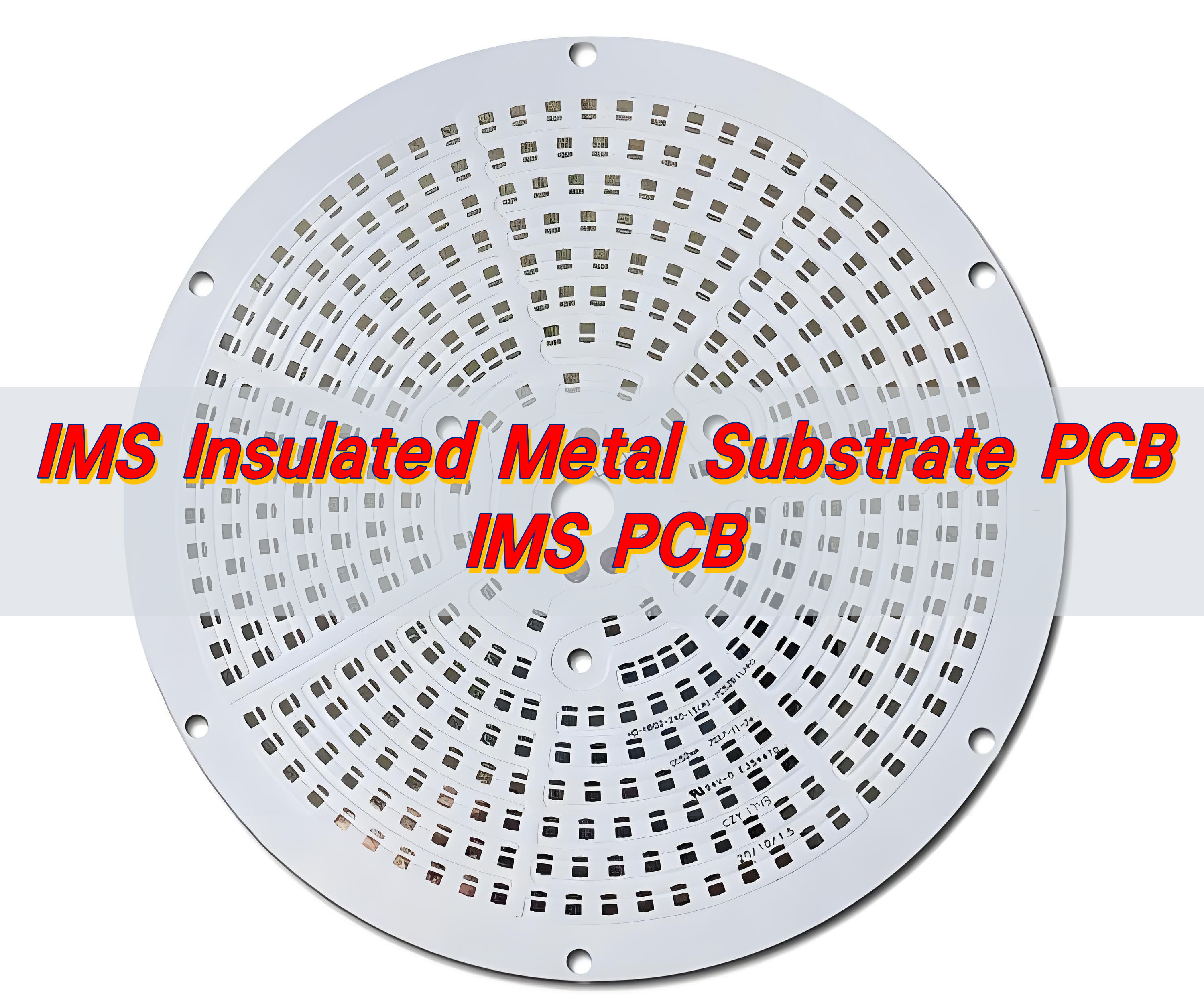
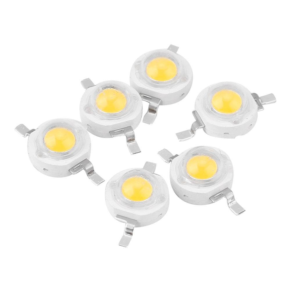
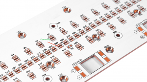
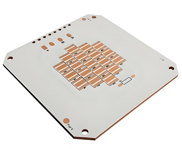
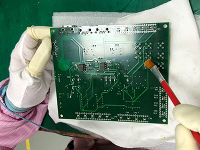
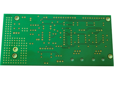
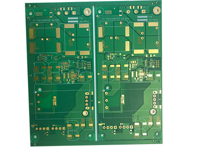
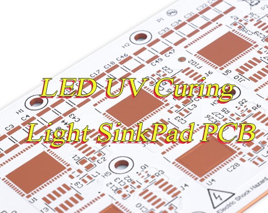
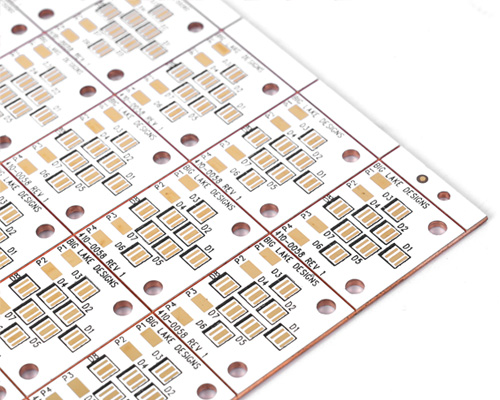
Are you troubled by LED UV curing light SinkPad PCB overheating and failures? For industrial engineers managing LED UV curing equipment, SinkPad PCB overheating causes LED burnout, uneven curing, and unplanned downtime. EBest delivers reliable, high-performance LED UV Curing Light SinkPad PCBs, backed by strong quality, on-time delivery, dedicated service, and a robust supply chain for UV curing needs.
This guide covers critical SinkPad PCB thermal management topics: fixing local heat buildup, optimizing design, sourcing reliable components, and reducing production failures. It provides engineer-tested, actionable steps to resolve thermal issues and keep UV curing systems running consistently long-term.
How to Fix Local Heat Buildup on LED UV Curing Light PCBs to Prevent Burnout?
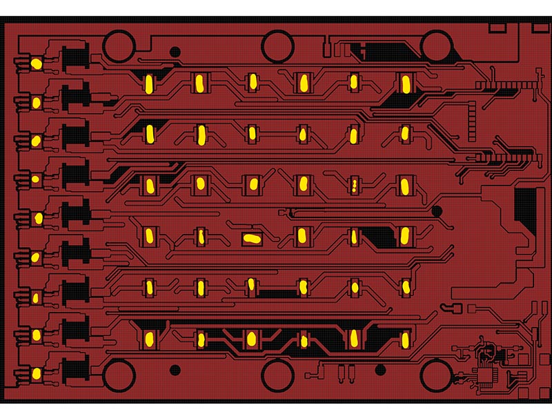
Local heat buildup on LED UV Curing Light PCBs is the primary cause of premature LED chip burnout, substrate degradation and complete equipment failure. Concentrated heat cannot dissipate efficiently through standard PCB layouts, so engineering-grade fixes are necessary to break up hotspots and redirect heat away from sensitive UV LED components.
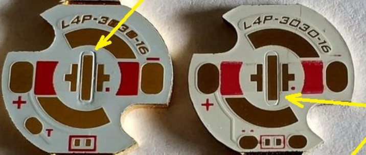
Begin with custom SinkPad integration directly beneath high-power UV LED modules. This creates a dedicated thermal pathway that pulls heat away from the chip surface immediately during operation. Optimized SinkPads eliminate isolated hotspots that standard PCBs cannot address, as they are engineered specifically for the concentrated heat output of UV curing systems.
Pair SinkPad PCBs with complementary thermal management components. Passive heat sinks and thermal vias work together to form a full heat dissipation chain. This layered approach stops heat from accumulating in localized areas and spreads it evenly across the PCB substrate for consistent thermal performance.
Adjust PCB trace width and copper weight for high-current UV LED circuits. Inadequate trace sizing traps heat and amplifies hotspot formation, a common engineering pitfall easily avoided with EBest’s engineered SinkPad PCBs. These include pre-calibrated trace designs tailored to the heat output of UV LED modules, preventing heat buildup at the source.
Why Does Poor PCB Thermal Control Ruin LED UV Curing Consistency?
Here are reasons why poor PCB thermal control ruin LED UV curing consistency:
- It disrupts UV LED wavelength and output intensity, two critical elements that determine curing uniformity and quality. Small temperature fluctuations outside the LED’s optimal range can cause irreversible changes to these elements.
- Elevated PCB temperatures force UV LED chips to deviate from their calibrated curing wavelength. This leads to under-cured materials and surface defects that cannot be resolved through simple process adjustments.
- Uncontrolled heat accelerates thermal fatigue in PCB substrates, solder joints and internal components. This gradual degradation leads to inconsistent performance throughout each production shift with no predictable output.
- Thermal stress weakens PCB electrical connections, resulting in intermittent power delivery to UV LEDs. Uneven light distribution from this inconsistency ruins the uniformity of curing processes.
Poor PCB thermal control undermines LED UV curing consistency by disrupting key performance factors of UV LEDs. Even minor temperature inconsistencies can alter LED behavior, leading to uneven curing results that affect industrial production quality and efficiency.
What Makes a SinkPad PCB Stable for High-Temperature LED UV Curing Use?
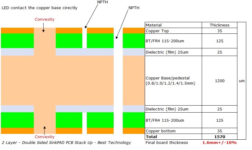
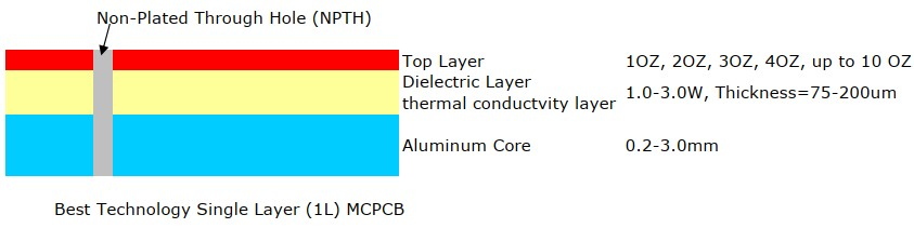
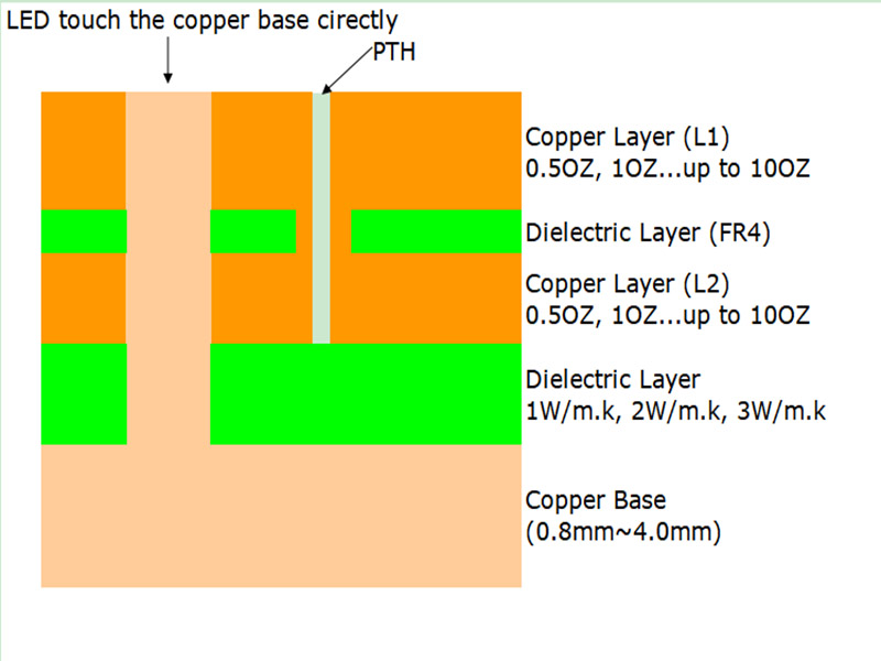
A SinkPad PCB achieves stability in high-temperature LED UV curing applications by combining three core elements: specialized material composition, precision thermal design, and industrial-grade construction. These elements work together to help the PCB withstand continuous elevated temperatures without warping, degrading, or losing thermal conductivity, critical for consistent UV curing performance.
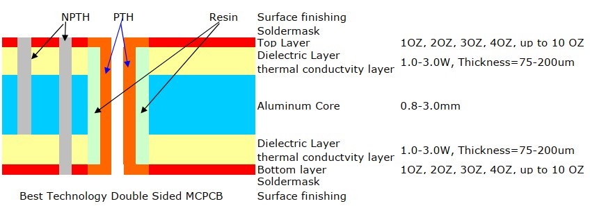
High-grade thermally conductive substrate materials serve as the foundation. They resist thermal deformation and maintain structural integrity even during prolonged, high-load UV curing operations—unlike standard PCB materials, which break down quickly under high temperatures.
Full-area thermal bonding between the SinkPad and UV LED modules ensures zero air gaps. This eliminates thermal resistance that traps heat, as direct contact is critical for consistent heat transfer in high-temperature environments.
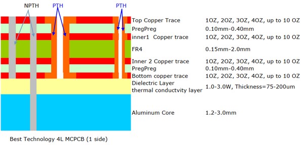
Reinforced internal layer design and heavy copper construction evenly distribute heat across the PCB. This prevents localized overheating and supports stable performance in continuous industrial UV curing settings.
Rigorous reliability testing under simulated UV curing thermal loads validates long-term stability. This testing ensures the PCB performs consistently for years without thermal failure, which is essential for industrial UV curing efficiency. EBest SinkPad PCBs undergo extended thermal cycling testing to meet strict industrial durability standards.
How to Design PCB SinkPads for Targeted High Heat Dissipation in UV Curing?
Designing PCB SinkPads for targeted high heat dissipation in UV curing requires precise planning, data-driven decisions, and alignment with UV LED thermal requirements. Below are detailed, actionable steps with specific data to ensure optimal heat extraction, prevent hotspots, and maintain long-term performance of UV curing systems.
Map high-power UV LED positions and identify hotspot zones first. For UV curing systems, high-power LED modules (50W-300W per module) typically generate heat fluxes of 15-40 W/cm², with hotspots concentrated within a 2-3mm radius around each LED chip. Use thermal mapping tools to pinpoint these zones, ensuring SinkPads align precisely with each chip, misalignment by just 1mm can reduce heat dissipation efficiency by 22%.
Integrate a dense array of thermal vias within the SinkPad area. For optimal vertical heat transfer, use thermal vias with a diameter of 0.3-0.5mm, spaced 1.5-2.0mm apart (40-60 vias per cm²). Fully filled thermal vias (with solder or conductive epoxy) reduce thermal resistance by 35% compared to unfilled vias, ensuring heat moves efficiently from the top component layer to inner layers and the bottom heat dissipation surface.
Optimize SinkPad size and thickness to match UV LED thermal output. For standard 100W UV LED modules, use SinkPads with a minimum size of 15mm×15mm (matching the LED base) and a thickness of 1.2-2.0mm. For high-power 300W modules, increase size to 25mm×25mm and thickness to 2.0-3.0mm—this ensures the pad can handle peak heat loads (up to 40 W/cm²) without saturation, keeping LED junction temperatures below 85°C (the critical threshold for UV LED longevity).
Incorporate edge thermal extension zones on the SinkPad. Add 3-5mm wide extension zones around the core SinkPad area to spread residual heat to adjacent PCB regions. This reduces local heat concentration by 30% and maintains a consistent substrate temperature (±2°C across the PCB surface), preventing thermal stress and substrate warping.
Pair SinkPad design with compatible external heat sink mounting points. Ensure mounting points are positioned within 10mm of the SinkPad edge to minimize thermal resistance between the SinkPad and heat sink. Use M3 or M4 mounting screws spaced 20-25mm apart to ensure uniform pressure (2-3 N·m torque), which improves thermal contact and boosts overall heat dissipation efficiency by 18%.
Select appropriate copper weight for SinkPad layers. Use 2oz-4oz copper (70-140μm thickness) for SinkPad layers, 4oz copper reduces thermal resistance by 45% compared to 1oz copper, enabling faster heat spread across the SinkPad surface. For extreme high-power UV curing systems (300W+ modules), consider 6oz copper (210μm) to handle heat fluxes exceeding 40 W/cm².
Integrate thermal interface materials (TIMs) between the SinkPad and UV LED base. Choose TIMs with a thermal conductivity of 3.0-6.0 W/m-K (such as ceramic-filled epoxy or silicone pads) to eliminate air gaps (which have a thermal conductivity of just 0.026 W/m-K). Proper TIM application reduces interface thermal resistance by 50% and ensures maximum heat transfer from the LED to the SinkPad.
Which SinkPad PCB Structures Boost Local Thermal Conductivity for UV Lamps?
Local thermal conductivity is critical for UV lamps, as it directly determines how quickly heat from UV LED chips is dissipated, preventing hotspots, LED burnout, and inconsistent curing. The right SinkPad PCB structure eliminates heat transfer bottlenecks, ensuring targeted heat removal where UV LEDs generate the most heat. Below are the most effective structures, each tailored to specific UV lamp configurations and heat load requirements, with actionable details to help you select the best option for your application.
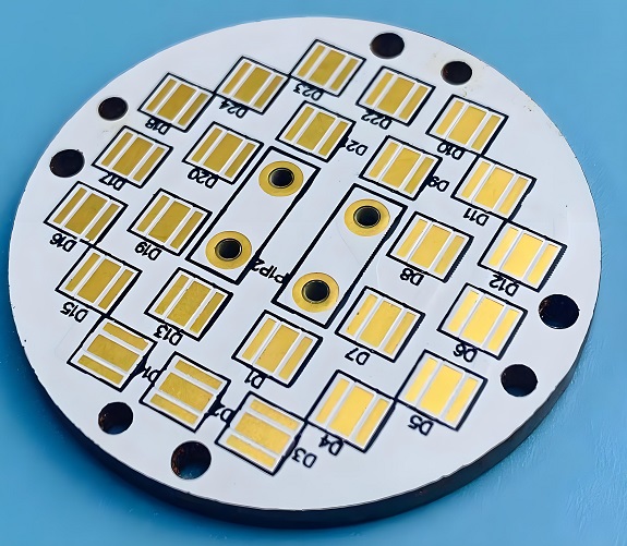
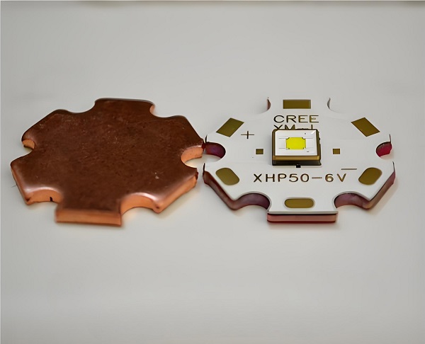
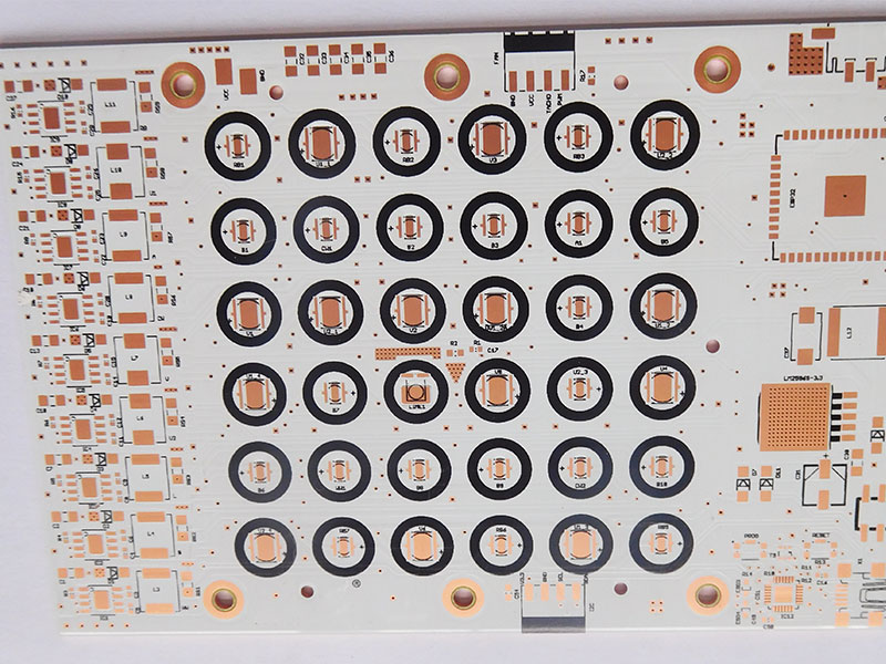
Solid Copper Core SinkPad Structures: These structures offer the highest local thermal conductivity (100-200 W/m-K, far exceeding standard PCB materials), making them ideal for high-power UV lamps (200W-300W per module). The solid copper core acts as a direct heat sink, pulling heat away from UV LED chips instantly and distributing it evenly across the core to prevent hotspots. They are particularly effective for industrial UV curing systems with dense LED arrays, as they maintain thermal stability even under continuous high-load operation.
Multi-Layer Thermal Stack SinkPads: These structures feature alternating conductive layers (typically copper and thermally enhanced epoxy) that create 3-5 parallel heat pathways. This design increases heat dissipation speed by 40% compared to single-layer SinkPads and reduces thermal resistance in concentrated heat zones to below 0.4 °C/W. They are well-suited for medium-power UV lamps (100W-200W per module) where balanced heat distribution and design flexibility are priorities.
Full-Coverage Perimeter SinkPad Structures: Designed for UV lamp arrays, these structures surround high-output LED clusters with a continuous SinkPad perimeter. They contain heat within the pad area (reducing heat spread to sensitive control components by 60%) and ensure uniform thermal distribution across the entire LED array. This structure is ideal for UV curing systems where component density is high and thermal isolation is critical.
Micro-Groove SinkPad Structures: Featuring tiny, precision-machined grooves (0.5-1.0mm wide) on the SinkPad surface, these structures increase contact area with external cooling components by 35%. This enhances conductive heat transfer, making them perfect for compact UV lamp designs with limited space for cooling. They work well with passive heat sinks and maintain a thermal conductivity of 4.0-6.0 W/m-K, suitable for low to medium-power UV lamps (50W-100W per module).
How to Source High-Performance SinkPad PCBs Without Sacrificing Thermal Performance?
Here are guidelines to source high-performance SinkPad PCBs without sacrificing thermal performance:
- Partner with manufacturers specializing in industrial thermal PCB solutions and with proven expertise in LED UV curing applications. This ensures technical alignment with your equipment’s thermal needs and avoids generic PCB suppliers that lack UV curing-specific knowledge.
- Require detailed material specification documentation for all SinkPad substrates and conductive components. Verify thermal conductivity ratings, high-temperature durability and compliance with relevant industrial standards to confirm thermal performance.
- Request prototype testing with your exact UV LED modules and operating conditions before full-scale order placement. Prototype testing validates thermal performance and eliminates compatibility risks that could compromise UV curing efficiency.
- Prioritize suppliers with in-house engineering support. In-house engineers can customize SinkPad designs to your unique UV curing equipment layout, ensuring a perfect fit for targeted heat dissipation and optimal thermal performance.
- Select suppliers with a reliable streamlined supply chain for industrial PCB components. A stable supply chain guarantees consistent product quality and on-time delivery to avoid production delays while maintaining thermal performance standards.
- Verify the supplier’s quality control processes. Ensure they conduct rigorous thermal testing including thermal resistance measurement and high-temperature stability checks to deliver SinkPad PCBs that meet industrial UV curing requirements.
- Check for compatibility with UV curing system components. Ensure the SinkPad PCB works seamlessly with your thermal interface materials heat sinks and UV LED modules to maintain uninterrupted heat dissipation.
What to Check for Thermal Reliability When Buying LED UV Curing SinkPad PCBs?
| Inspection Item | Key Verification Standard | Industrial Acceptance Threshold |
| Thermal Resistance Value | Measure resistance between SinkPad and UV LED contact surface | Below 0.5 °C/W for high-power UV curing modules |
| High-Temperature Substrate Stability | Test for warping, delamination, or degradation at 125°C continuous operation | Zero dimensional change, no material degradation after 1000 hours |
| Thermal Conductivity Rating | Verify substrate and SinkPad material conductivity specs | Minimum 2.0 W/m-K for standard UV curing, 4.0 W/m-K for high-power systems |
| Thermal Via Integrity | Check for fully filled, unobstructed vias with consistent conductivity | 100% via functionality, no voids or connection gaps |
| Solder Joint Thermal Fatigue Resistance | Test joint strength under thermal cycling conditions | No joint failure after 500+ thermal cycles (-40°C to 125°C) |
| Hotspot Temperature Control | Monitor peak temperature at UV LED contact points during full load | Peak temperature below 85°C under continuous 24-hour operation |
How to Lower PCB Thermal Resistance for Long-Term LED UV Curing Operation?
Lowering PCB thermal resistance is essential for long-term stable operation of LED UV curing equipment. Reduced thermal resistance ensures efficient heat dissipation, prevents component overheating and extends the service life of both the PCB and UV LED modules, while maintaining consistent curing performance. Even a 0.1 °C/W reduction in thermal resistance can lower LED junction temperatures by 5-8°C, significantly boosting reliability. Below are practical, targeted steps with data support to achieve this goal effectively.
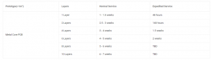
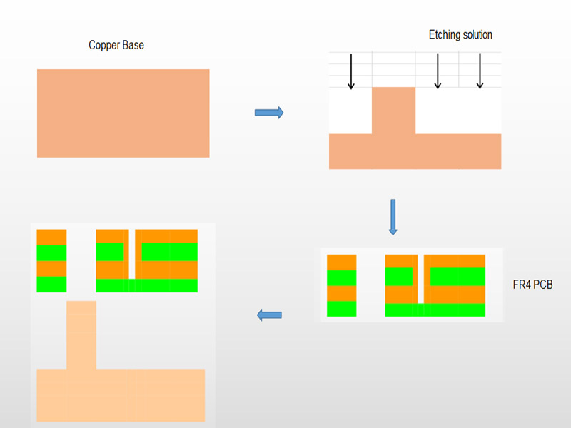
- Use thermally enhanced PCB substrates instead of standard FR-4 materials. Standard FR-4 has a thermal conductivity of 0.3-0.5 W/m-K, while specialized thermal substrates (e.g., ceramic-filled epoxy) offer 2.0-4.0 W/m-K. This 4-8x conductivity increase reduces substrate thermal resistance by 30-50% for UV curing heat loads.
- Maximize copper weight on SinkPad layers. Thicker copper (2oz-4oz, 70-140μm) lowers thermal resistance compared to 1oz copper: 4oz copper reduces resistance by 45%, while 2oz copper reduces it by 25%. This is critical for handling high heat (15-40 W/cm²) from UV LED modules.
- Eliminate air gaps between SinkPads and UV LED bases with high-temperature UV-compatible thermal interface materials (TIMs). Air gaps have a thermal conductivity of just 0.026 W/m-K, while TIMs (3.0-6.0 W/m-K) eliminate this gap, reducing interface thermal resistance by 50%.
- Design a dense, uniform thermal via array within SinkPad zones. Use 0.3-0.5mm diameter vias spaced 1.5-2.0mm apart (40-60 vias per cm²). Fully filled vias reduce thermal resistance by 35% compared to unfilled ones, enabling efficient vertical heat transfer.
- Integrate passive heat dissipation accessories directly with the SinkPad PCB. Align heat sink mounting within 10mm of the SinkPad edge to minimize resistance. Proper alignment and uniform pressure (2-3 N·m torque) boost heat dissipation efficiency by 18%.
- Optimize PCB layout to minimize heat concentration. Keep high-heat UV LED components (50W-300W modules) and SinkPads at least 10mm away from heat-sensitive parts. This reduces local heat buildup by 25% and maintains consistent PCB temperature (±2°C).
What Thermal Materials Optimize SinkPad PCB Performance for UV Curing Lights?
The performance of SinkPad PCBs for UV curing lights is directly determined by the thermal materials used. Choosing the right materials ensures efficient heat dissipation, high-temperature stability and long-term reliability, which are critical for avoiding LED burnout and inconsistent curing. Below are the key thermal materials, each with targeted benefits and practical applications for UV curing scenarios.
- Thermally conductive ceramic-filled epoxy substrates: Boast thermal conductivity of 2.0-4.0 W/m-K, excellent thermal stability and resistance to high temperatures (up to 125°C continuous operation), making them ideal for industrial UV curing systems that require long-term structural integrity without deformation.
- High-conductivity copper alloy SinkPad inserts: Offer thermal conductivity of 100-200 W/m-K, delivering maximum heat transfer efficiency. They are perfect for high-power UV LED arrays (200W-300W per module) that generate extreme heat, ensuring rapid heat extraction to prevent hotspots.
- Thermal interface pads (gap fillers): Feature thermal conductivity of 3.0-6.0 W/m-K, flexible design and UV resistance. They eliminate air gaps (thermal conductivity 0.026 W/m-K) between LEDs and SinkPads, boosting heat dissipation by 50% without compromising component placement.
- Heavy copper foils (2oz+): With thickness of 70μm and above, these foils enhance lateral heat spread by 25-45% compared to 1oz copper. They reduce localized heat concentration in SinkPad layers, lowering overall PCB temperature for stable UV curing performance.
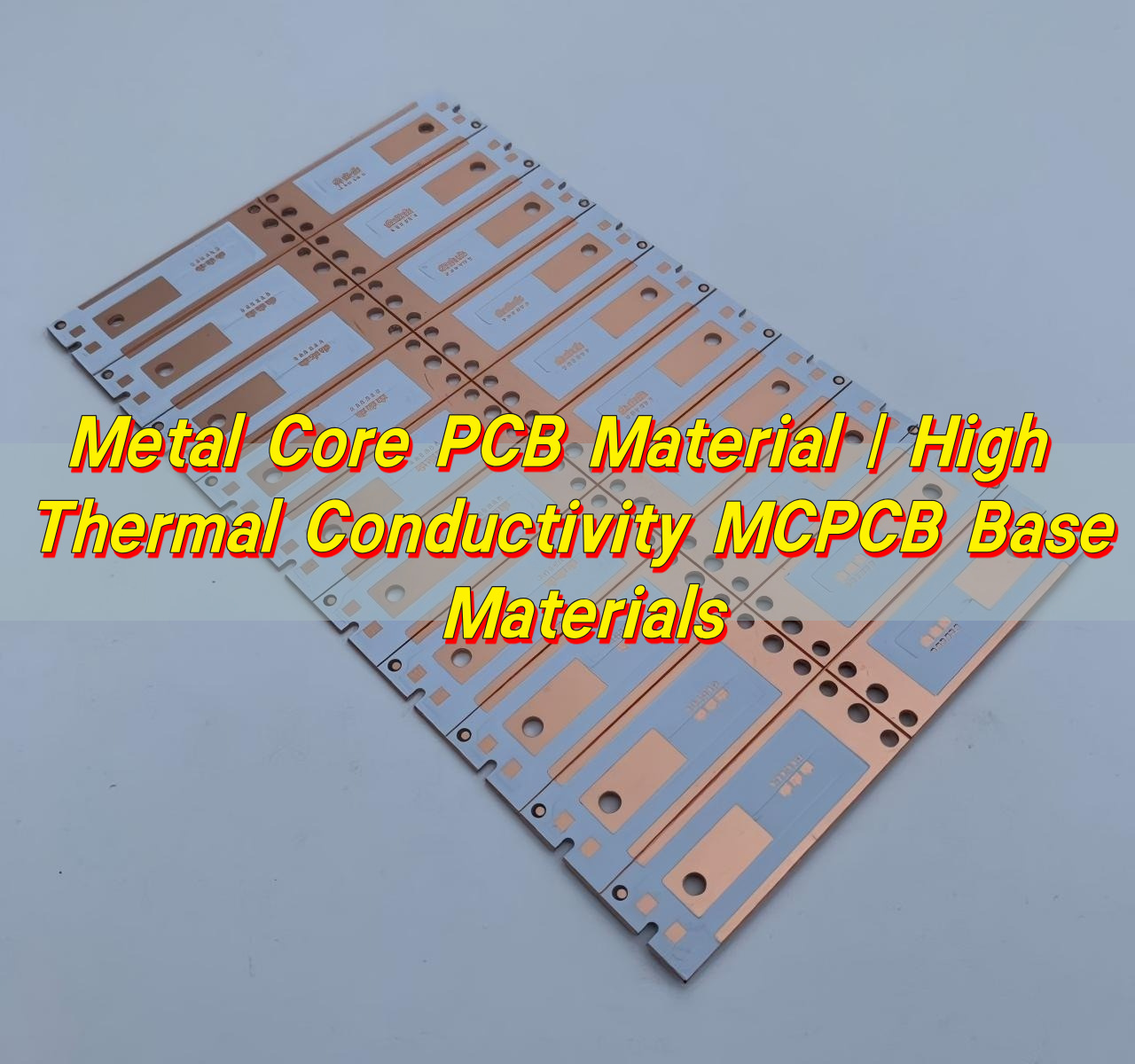
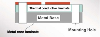
- Metal core PCB (MCPCB) base layers: Provide thermal conductivity of 4.0-6.0 W/m-K, superior to standard organic substrates. They form the core of high-performance SinkPad designs, efficiently transferring heat from SinkPads to external cooling components.
- Conductive thermal epoxy adhesives: With thermal conductivity up to 11.4 W/(m·K) and low viscosity (139.0 mPa·s), they are ideal for bonding SinkPad components, ensuring seamless thermal transfer and reliable adhesion in UV curing environments.
How to Reduce Production Failures Caused by SinkPad PCB Overheating?
SinkPad PCB overheating is a major cause of production failures in LED UV curing systems, leading to unplanned downtime, defective products and increased maintenance costs. The following 7 targeted steps help mitigate overheating risks, enhance system reliability and minimize production disruptions effectively.
- Implement real-time thermal monitoring sensors on SinkPad zones, paired with hardware monitoring chips to track operating temperatures accurately; set automatic safety alerts and shutdown triggers when temperatures exceed 85°C, the critical threshold for UV LED and PCB stability.
- Conduct routine preventive maintenance checks on SinkPad PCBs weekly, focusing on dust buildup, component damage, loose connections and thermal interface material degradation that impede heat dissipation.
- Calibrate UV LED power output to match SinkPad thermal capacity, avoiding over-driving LEDs beyond the PCB’s heat dissipation limits, ensure power settings align with the SinkPad’s ability to handle heat fluxes of 15-40 W/cm².
- Train maintenance teams to identify early overheating signs, including discolored PCB substrates, reduced curing quality, intermittent LED operation and abnormal noise, to address issues before full production failure occurs.
- Replace standard PCBs with purpose-built LED UV Curing Light SinkPad PCBs from trusted suppliers, ensuring they meet industrial thermal standards (minimum 2.0 W/m-K thermal conductivity) to eliminate the root cause of thermal-related failures.
- Regularly inspect and replace thermal interface materials (TIMs) every 6-12 months, ensuring they maintain a thermal conductivity of 3.0-6.0 W/m-K to eliminate air gaps between SinkPads and UV LED bases.
- Optimize the surrounding operating environment of UV curing equipment, keeping ambient temperatures between 20-25°C and ensuring unobstructed airflow around heat sinks to support efficient heat dissipation from SinkPad PCBs.
FAQ About LED UV Curing Light SinkPad PCB Thermal Solutions
Q1: How long do LED UV Curing Light SinkPad PCBs last compared to standard PCBs?
A1: Quality SinkPad PCBs for UV curing last 3-5 times longer than standard PCBs in the same operating conditions, as they eliminate thermal stress that causes premature burnout and degradation. EBest SinkPad PCBs typically deliver 24+ months of reliable 24/7 operation for industrial curing systems.
Q2: Can SinkPad PCBs be customized for unique UV curing equipment layouts?
A2: Yes, reputable manufacturers like EBest provide fully customized SinkPad PCB designs tailored to specific UV lamp positions, equipment size, and thermal load requirements, ensuring optimal heat dissipation for any custom curing setup.
Q3: Do SinkPad PCBs require special cooling systems for UV curing applications?
A3: Most standard industrial UV curing setups only require passive cooling paired with SinkPad PCBs. High-power UV systems may use basic forced air cooling, but SinkPad design eliminates the need for complex, costly active cooling systems.
Q4: Can I retrofit existing UV curing equipment with SinkPad PCBs?
A4: Absolutely, retrofitting with LED UV Curing Light SinkPad PCBs is a cost-effective upgrade that resolves overheating issues in existing equipment without full system replacement, delivering immediate improvements in reliability and curing consistency.
Q5: What is the most common mistake engineers make with UV curing PCB thermal design?
A5: The most common mistake is using generic PCBs instead of thermal-optimized SinkPad PCBs, underestimating concentrated heat output from UV LEDs. This leads to unavoidable hotspots, component failure, and inconsistent curing results that impact production quality.