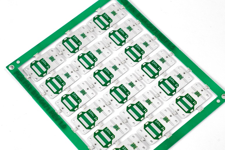
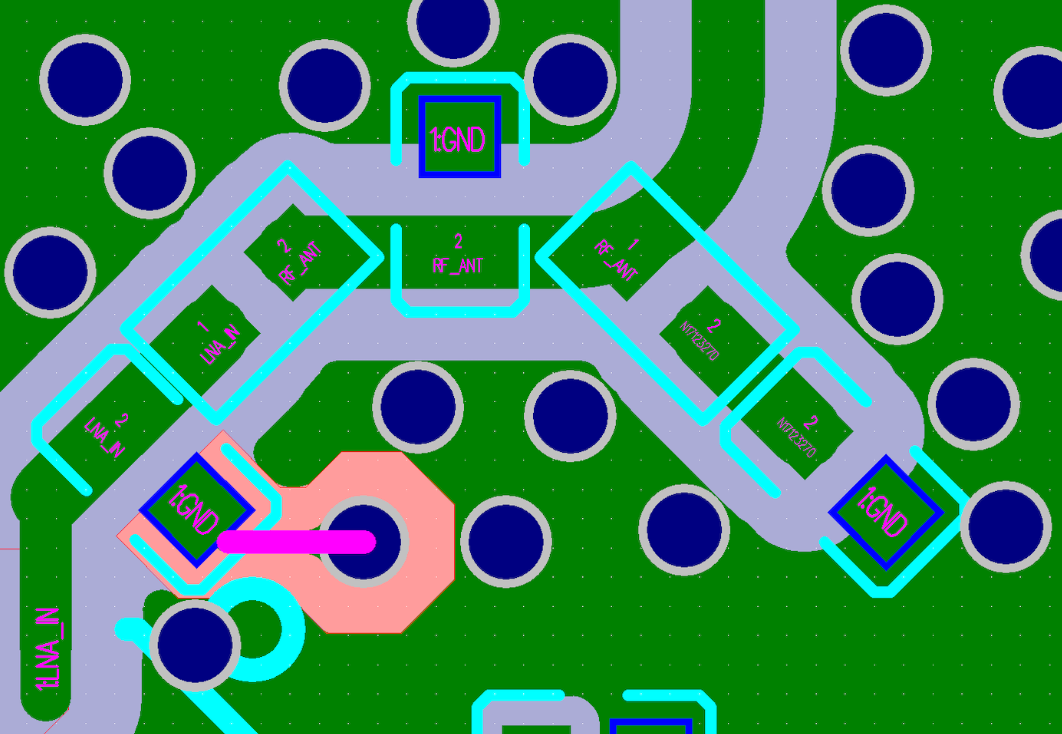
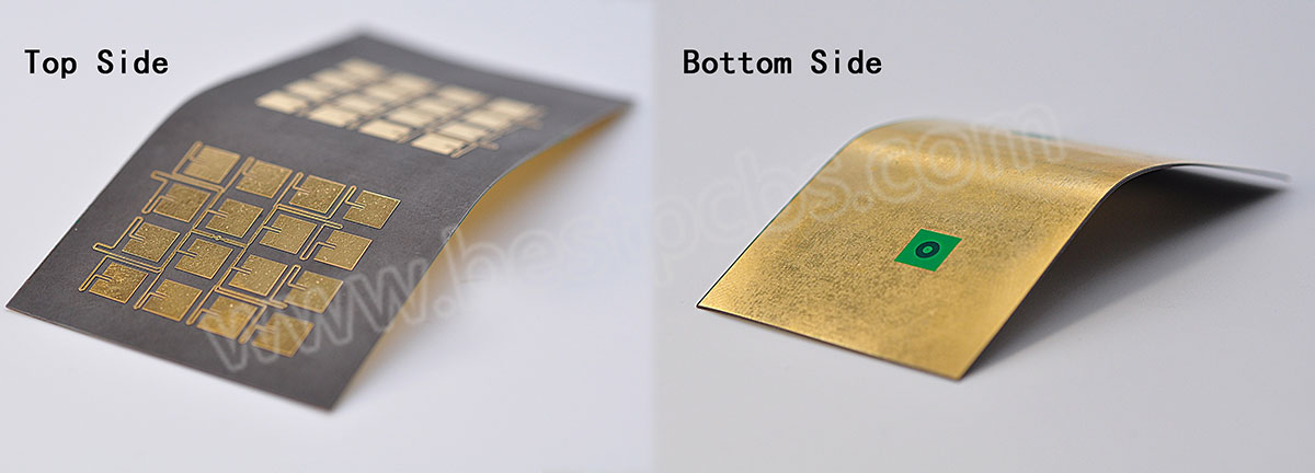
RF board, or Radio Frequency Printed Circuit Board, is engineered for circuits operating at high frequencies where signal integrity becomes highly sensitive to material properties. Typical RF designs work in the range of 300 MHz to 3 GHz, and many advanced systems extend far beyond this.
At these frequencies, standard FR4 materials often fail to maintain stable dielectric performance and low signal loss. As a result, specialized high frequency laminates are required. RF PCBs are therefore built using materials with low dielectric loss (Df) and stable dielectric constant (Dk) to ensure consistent signal transmission.
RF board is ideal for applications with higher operating frequency requirements. Right now, we normally use following material:
These boards are widely used in applications such as:
Wireless communication systems
RF antennas and modules
Automotive radar (ADAS)
Satellite and aerospace electronics
Microwave devices
IoT and high-speed signal systems
Why Use RF PCB Instead of Standard FR4?
FR4 is cost-effective and widely used, but its dielectric properties vary significantly at high frequencies. This leads to signal loss, impedance instability, and reduced system reliability in RF designs.
More stable dielectric constant across frequency range
Better impedance control
Reduced signal distortion
Improved phase consistency
What Materials Are Used in RF PCB?
Material selection is the core of RF PCB performance. Different applications require different dielectric properties and processing characteristics.
Common RF PCB Materials
1. Rogers Laminates
Widely used in RF and microwave circuits due to balanced performance and manufacturability.
Typical grades include:
RO4003C
RO4350B
RO4233
These materials offer:
Stable dielectric constant
Low loss tangent
Good thermal reliability
2. PTFE-Based Materials (Teflon)
Used in more demanding RF designs where ultra-low loss is critical.
Advantages:
Extremely low dielectric loss
Excellent high frequency performance
Considerations:
More complex processing
Higher manufacturing cost
Copper Thickness Range
Standard: 1/4 oz to 2 oz
Custom: based on current load and thermal design
Rogers is often the practical choice for most RF designs, while PTFE is used when performance requirements are more demanding.
Rogers Laminate Material Parameters
Choosing the right Rogers material directly affects signal integrity, impedance stability, and insertion loss. Below is a comparison of commonly used Rogers laminates for RF PCB applications.
Material
Dielectric Constant (Dk @10GHz)
Loss Tangent (Df @10GHz)
Thermal Conductivity (W/m·K)
Typical Application
RO4350B
3.48 ±0.05
0.0037
0.62
General RF, antennas, automotive radar
RO4003C
3.55 ±0.05
0.0027
0.71
RF communication, microwave circuits
RO4233
3.30 ±0.05
0.0025
0.65
High frequency, low loss applications
RT5880
2.20 ±0.02
0.0009
0.20
Ultra-low loss, aerospace, high-end RF
RO3003
3.00 ±0.04
0.0013
0.50
High stability circuits, precision RF
RO3010
10.2 ±0.25
0.0023
0.95
High dielectric designs, compact circuits
RF Board Capability
Base material: Rogers/Telfon
Board Thickness: 0.5mm~3.0mm(0.02″~0.12″)
Copper thickness: 0.5 OZ, 1.0 OZ, 2.0 OZ, 3.0 OZ
Outline: Routing, punching, V-Cut
Soldermask: White/Black/Blue/Green/Red Oil
Legend/Silkscreen Color: Black/White
Surface finishing: Immersion Gold, HASL, OSP
Max Panel size: 600*500mm(23.62″*19.68″)
Packing: Vacuum/Plastic bag
Samples L/T: 7~9 Days
MP L/T: 8~10 Days
RF PCB FAQs
1. What frequency requires RF PCB instead of FR4?
Typically, designs above 1 GHz or requiring strict impedance control should consider RF materials. Lower frequencies may still use FR4 depending on performance tolerance.
2. Is Rogers better than FR4?
For high frequency applications, yes. Rogers offers lower loss and more stable dielectric properties, which improves signal integrity.
3. Why is PTFE PCB more expensive?
PTFE materials are harder to process and require specialized manufacturing steps, which increases production cost.
4. Can RF PCB be used for mixed signal designs?
Yes. Hybrid stackups combining RF materials and FR4 are commonly used to balance performance and cost.
Start Your RF PCB Project Today
If you are designing RF or microwave circuits, choosing the right PCB is critical to performance.
At Best Technology, we combine material expertise, process control, and engineering support to deliver reliable RF PCB solutions.
An RF board is a specialized printed circuit board designed to transmit and process radio-frequency signals ranging from 3 kHz to 300 MHz, and in many practical designs extending into the microwave range from 300 MHz up to 300 GHz, where signal integrity, low transmission loss, and precise impedance control are mandatory for reliable operation.
What are the most common obstacles in sourcing and deploying a reliable RF microwave PCB board?
Material Missteps: Using standard FR-4 at GHz frequencies causes excessive dielectric loss and unstable thermal performance.
DFM Gaps: RF circuit board designs pass simulation but fail in production due to unrealistic tolerances.
Inconsistent Fabrication Quality: Poor process control leads to impedance variation, copper roughness, and delamination.
Supply Chain Risks: Difficulty sourcing RF boards that consistently meet military or UL/CE compliance.
Insufficient Testing: Basic inspections miss critical RF board test issues such as PIM or resonance.
The solution lies in collaborating with a specialist fabricator whose entire process is engineered for high-frequency success.
Expert Material Selection: Choose proven RF laminates such as Rogers or Taconic, including metal-backed options when required.
Early DFM Collaboration: Involve the fabricator during RF board layout to ensure manufacturable stack-ups and vias.
Precision Manufacturing Processes: Apply LDI, plasma desmear, and controlled impedance etching for high-frequency accuracy.
Certified Production Lines: Work with suppliers qualified for mil-spec and regulated RF board production.
Advanced RF Testing: Verify performance using TDR, S-parameter analysis, and PIM testing for telecom applications.
This article explores the intricate world of RF and microwave PCB design, material science, and manufacturing, providing a roadmap for achieving reliability in the most demanding applications. BEST Technology is a specialized manufacturer of high-precision, high-frequency PCBs. We combine deep material science knowledge with state-of-the-art fabrication and testing facilities to transform complex microwave and RF designs into reliable, production-ready hardware. From RF prototype boards to high-volume runs, we ensure your board performs as simulated. Pls feel free to contact our experts at sales@bestpcbs.com to start your project.
What Is the Definition of an RF Board?
An RF (Radio Frequency) board is a specialized printed circuit board engineered to transmit, route, and process electromagnetic signals in the radio frequency spectrum, generally covering 3 kHz to 300 MHz. Within this range, signal behavior transitions from low-frequency electrical conduction to wave-dominated propagation, requiring controlled impedance, stable dielectric properties, and careful layout discipline.
When operating above 300 MHz, PCB designs enter the microwave domain, which typically spans 300 MHz to 300 GHz. At these frequencies, an RF board must function as a guided transmission structure rather than a simple interconnect, making dielectric constant (Dk), dissipation factor (Df), copper surface roughness, stack-up symmetry, and grounding strategy critical to performance.
Unlike standard digital PCBs, RF and microwave boards are designed around signal integrity, insertion loss, phase stability, and electromagnetic compatibility, ensuring predictable behavior across the intended frequency band and operating environment.
Why Microwave Systems Rely on Specialized Microwave PCBs Instead of Standard FR-4 Boards?
At microwave frequencies, the electrical properties of the PCB substrate become the dominant factor in performance. Standard FR-4 is unsuitable due to:
High Dielectric Loss (Df): Absorbs signal energy, converting it to heat and severely attenuating the signal.
Inconsistent Dielectric Constant (Dk): Varies with frequency and lot-to-lot, making stable impedance matching impossible.
High Moisture Absorption: Changes electrical properties and can lead to delamination.
Poor Thermal Conductivity: Inefficient for heat dissipation from active RF power amplifier components.
Specialized microwave PCBs use engineered laminates (e.g., PTFE-based ceramics, hydrocarbon ceramics) that offer low loss, stable Dk, low moisture absorption, and often better thermal performance, which is essential for reliable RF circuit board operation.
What Materials and Stackups Are Best Suited for an RF Circuit Board Operating at GHz Frequencies?
Material selection is the first critical decision for a successful RF PCB.
Material Type
Typical Brands
Key Properties
Best For
PTFE/ Ceramic
Rogers RO4000®, Taconic RF-35
Low loss, stable Dk, good performance
Multi-layer boards, digital analog integration
Pure PTFE
Rogers RT/duroid®
Ultra-low loss, excellent electrical stability
Critical RF amplifier board, aerospace
Hydrocarbon Ceramic
Rogers RO3000®
Low loss, good thermal conductivity
Metal core boards for high power
Thermoset Hydrocarbon
Isola IS680-350
Cost-effective, lower loss than FR-4
Consumer RF module board
A optimal RF board stackup for GHz frequencies should:
Use a low-loss core material for RF layers.
Implement a symmetrical stackup to prevent warpage.
Minimize the distance between RF signal and reference planes to reduce radiation.
Use multiple ground vias (stitching) around RF lines to suppress cavity resonances.
Consider hybrid stackups (e.g., FR-4 for digital, Rogers for RF) for cost-sensitive, mixed-signal designs.
What Is RF Circuit Board Design?
RF circuit board design is the discipline of laying out a PCB to effectively manage high-frequency electromagnetic waves. It transcends simple connectivity, focusing on controlling the behavior of signals as they travel along transmission lines. Core principles include:
Controlled Impedance: Ensuring signal traces have a consistent characteristic impedance (e.g., 50Ω) to prevent reflections.
Transmission Line Theory: Using microstrip or stripline geometries rather than simple “wires.”
Minimizing Discontinuities: Carefully managing bends, vias, and component pads to avoid parasitic inductance/capacitance.
Isolation and Shielding: Strategic use of grounding, board level EMI RF shields, and spacing to prevent crosstalk and radiation.
Thermal Management: Providing adequate heat sinking for active components, often integrated into the RF board layout.
What Is the Application of RF Circuit Board?
RF circuit boards are the enabling technology for wireless connectivity and signal processing across industries.
Telecommunications: 5G/6G base stations, satellite comms equipment, and microwave backhaul links.
Aerospace & Defense: Radar systems, electronic warfare (EW), and avionics requiring suppliers for military specs.
Automotive: Advanced driver-assistance systems (ADAS), vehicle-to-everything (V2X), and GPS.
Medical: MRI machines, therapeutic and diagnostic equipment, and wireless monitoring devices.
Consumer Electronics: Smartphones, Wi-Fi routers, and gaming consoles (e.g., xbox one RF board replacements).
Best HDI PCB Manufacturers for RF and Microwave Circuit Boards
Based on 2024–2025 industry data and global market research, the following companies stand out as the world’s leading HDI (High-Density Interconnect) PCB manufacturers for RF (Radio Frequency) and Microwave applications. These manufacturers demonstrate proven capabilities in ultra-fine line processing, controlled impedance, high-layer HDI builds, and maintain robust certification systems tailored to high-frequency and high-reliability sectors.
🏆 Overall Market Leader
TTM Technologies | United States Global HDI Market Leader for RF and Microwave Applications
TTM Technologies is one of the world’s largest HDI PCB manufacturers, widely recognized for its advanced RF and microwave capabilities across aerospace, defense, telecommunications, and automotive electronics. Its long-term investment in signal integrity engineering and high-layer HDI platforms positions it as a benchmark supplier for mission-critical RF designs.
🇨🇳 China Market Leader
EBest Circuit (Best Technology) | China Core Supplier for AI Servers and 5G Infrastructure
EBest Circuit (Best Technology) plays a dominant role in AI computing infrastructure and advanced communication systems. It is a key PCB supplier for autonomous driving platforms and high-performance computing, with strong HDI and RF manufacturing depth supporting large-scale production.
Note: Manufacturer selection is based on Prismark market data and a combined evaluation of RF/microwave process barriers, certification depth, and market share.
TTM Technologies (USA)
RF and Microwave Expertise TTM demonstrates exceptional process maturity in millimeter-wave frequencies and high-frequency signal integrity control, making it a preferred supplier for aerospace and defense RF platforms.
Certification Strength The company holds Nadcap accreditation, a critical aerospace qualification that many general PCB manufacturers cannot meet, reinforcing its position in high-reliability markets.
AT&S (Austria)
Automotive RF Leadership AT&S excels in ADAS, automotive radar, and electric vehicle RF systems, where long-term reliability and thermal stability are mandatory.
Quality and Sustainability Its operations emphasize renewable energy usage and strict compliance with IATF 16949, aligning with global automotive OEM requirements.
Unimicron (Taiwan)
Miniaturization Capability With trace and space down to 2/2 μm, Unimicron is well-suited for compact, highly integrated RF modules used in smartphones and wireless devices.
Advanced Interconnect Technology Its strength in ALIVH (Any-Layer Interstitial Via Hole) technology supports complex RF stackups and dense interconnections.
Market Landscape and Industry Trends
Estimated Global HDI Market Share
Compeq: 11%
Unimicron: 11%
TTM Technologies: 10%
AT&S: 7.7%
Other manufacturers: 60%
Data source: Prismark 2024 global HDI market report. The listed companies represent the core share holders in RF and microwave HDI manufacturing.
Practical Selection Recommendations
When selecting an HDI PCB manufacturer for RF and microwave applications, consider the following guidance:
Aerospace or military-grade systems Prioritize TTM Technologies or AT&S, as both maintain AS9100 and Nadcap certifications.
Automotive radar and ADAS platforms AT&S offers the most comprehensive automotive-focused RF certification portfolio.
Consumer electronics and 5G infrastructure Unimicron or Compeq provide high-precision RF manufacturing with competitive cost structures.
Ultra-thin or high-layer RF designs Meiko Electronics delivers unique advantages in precision HDI and long-term manufacturing stability.
Top Companies for RF Microwave PCB and Metal Core Boards
Based on the latest industry data and search insights, the following five companies are widely recognized as global leaders in RF/Microwave and Metal Core PCB manufacturing. Their market position is driven by strong capabilities in high-frequency material processing, precision fabrication, and strict certification systems, enabling them to serve demanding applications across aerospace, defense, telecom, automotive, and high-power electronics.
🌍 Global High-End Manufacturers
Advanced Circuitry International (ACI)
United States | RF/Microwave Specialist
Core Strengths ACI focuses exclusively on RF and microwave antenna PCB manufacturing, with more than 30 years of industry experience supporting high-reliability programs.
RF Capabilities The company is well known for large-format PCB fabrication, blind and buried vias, and advanced Ohmegaply™ hybrid constructions, enabling excellent impedance stability and thermal control.
Material Support Extensive experience with Rogers, Taconic, Arlon, and other premium RF laminates.
Certifications ISO 9001, AS9100D, ITAR registered.
Teledyne Labtech
UK / USA | Military and High-Reliability Applications
Core Strengths Teledyne Labtech delivers solutions for military and harsh commercial environments, including advanced technologies such as embedded graphite layers for thermal management.
RF Capabilities Full-size PCB manufacturing, antenna fabrication, and integrated thermal control solutions for RF and microwave systems.
Certifications ISO 9001, ISO 14001, JOSCAR.
🇨🇳 Asia-Based Supply Chain Leaders
EBest Circuit (Best Technology)
China | Comprehensive PCB and Assembly Services
Core Strengths EBest Circuit (Best Technology) provides one-stop manufacturing services, covering both metal core PCB fabrication and complete PCBA assembly.
Metal Core Capability Manufactures single-layer and multilayer aluminum- and copper-based metal core boards, suitable for power electronics and thermal-intensive designs.
Certifications UL, IATF 16949, ISO 9001, ISO 13485, AS9100D CE, RoHS.
ISO 9001, ISO 13485, IATF 16949, AS9100D, UL, REACH, and RoHS.
How to Select the Right RF Microwave PCB Board Supplier for High-Reliability Industries
Choosing a RF microwave pcb board supplier for medical, aerospace, or defense applications requires due diligence.
Audit Quality Systems: Review their AS9100 or ISO13485 certifications and audit reports.
Evaluate Technical Support: Assess their engineers’ ability to discuss RF board design guidelines and material trade-offs.
Inspect Testing Capabilities: Ensure they have the required RF board test equipment (e.g., TDR, network analyzer, flying probe).
Review Documentation: Request examples of travel coupons, test reports, and material certifications.
Check Industry References: Ask for case studies or contacts in your specific field (e.g., medical devices, telecom networks).
How Do You Streamline RF Board Installation for High-Reliability Designs?
Streamlining RF board installation prevents field failures. Key practices include:
Clear Mechanical Documentation: Provide detailed drawings showing keep-out areas, shield placement, and torque specs for board to board RF connectors.
Integrated Alignment Features: Design in tooling holes, dowel pins, or guides for error-free assembly.
Standardized Connectorization: Use common, reliable RF board to board connector types to simplify cabling.
Comprehensive Assembly Instructions: Create visual work instructions covering handling, ESD, soldering, and cleaning.
On-Board Test Points: Include accessible coaxial test points for validation during system integration.
What Testing and Validation Methods Are Required for Reliable RF Board Test Results?
A robust RF board test protocol is essential for reliability.
Automated Optical Inspection (AOI): Checks for surface defects and solder issues.
Controlled Impedance Testing: Uses a Time Domain Reflectometer (TDR) to verify trace impedance meets design specs (e.g., 50Ω ±10%).
Network Analysis: Measures S-parameters (S11, S21) to validate insertion loss, return loss, and isolation across the operational bandwidth.
High-Potential (HiPot) Testing: Ensures dielectric strength and electrical isolation.
Specialized Tests: May include passive intermodulation (PIM) testing for telecom, or thermal cycling for environmental robustness.
Where to Get RF Microwave PCB Boards Metal-Backed?
Metal-backed PCBs (also called metal-clad or insulated metal substrates) are ideal for high-power RF applications. They are available from specialized fabricators who:
Offer Various Metals: Typically aluminum (for cost and weight) or copper (for best thermal performance).
Handle Dielectric Bonding: Expertly laminate a thin, thermally conductive but electrically insulating dielectric layer to the metal base.
Manage CTE Mismatch: Use processes that prevent warping or delamination during thermal cycling.
Provide Secondary Operations: Offer machining, tapping, and anodizing of the metal base as part of the service.
Why EBest Circuit (Best Technology) Is the Best Partner for RF Boards Fabrication?
EBest Circuit (Best Technology) distinguishes itself as a leader in the fabrication of complex Radio Frequency (RF) and Microwave printed circuit boards. Our expertise is demonstrated through hard process data, advanced engineering capabilities, and full control over the manufacturing value chain.
1. Mastery of High-Frequency Materials
We specialize in processing a wide range of advanced substrates critical for RF performance, ensuring optimal signal integrity and controlled dielectric properties.
Material Portfolio: Expertise in Rogers (e.g., 4350B, 4003), PTFE (Taconic, Arlon), and ceramic-filled materials (M-series).
Layer Count: Capable of manufacturing highly complex multilayer boards up to 50 layers (standard), with advanced capabilities for up to 100 layers (upon review).
2. Precision Engineering for Critical RF Parameters
Our processes are calibrated to meet the tight tolerances required for high-frequency applications.
Fine Lines/Spacing: Standard outer layer trace/space of 3.5/4 mil for 1oz copper, with advanced capabilities down to 3/3 mil.
Micro-Vias & Drilling: Laser drilling for HDI designs down to 0.07mm. Exceptional mechanical drill hole position accuracy of ±0.05mm.
Controlled Impedance: Industry-leading impedance control with tolerances as tight as ±4Ω (for impedances <50Ω) or ±6% (for impedances ≥50Ω).
RF-Suitable Surface Finishes: Including ENIG (Nickel: 3-8µm, Gold: 0.025-0.125µm), Immersion Silver, and OSP.
3. Uncompromising Quality and Reliability
We ensure board performance and reliability through stringent process controls.
Layer-to-Layer Registration: Advanced registration control of ≤0.13mm.
Solder Mask Alignment: Precision alignment tolerance of ±0.05mm.
Board Flatness: Superior warpage control, with a capability of 0.005.
To sum up, EBest Circuit (Best Technology) provides a proven foundation for your most demanding RF applications, backed by concrete data in high-frequency material processing (Rogers/PTFE), complex stack-ups (to 50L), fine features (3/3 mil), tight impedance control (±4Ω), and precision drilling (0.07mm laser vias).
All in all, RF Boards are the precision-engineered backbone of modern wireless systems, where every micron and material property dictates performance. This guide has navigated the critical aspects of RF and microwave PCB design, manufacturing, and validation, emphasizing the partnership required to achieve reliability.
For projects where performance cannot be compromised, partnering with a specialist is paramount. BEST Technology provides that essential edge, combining deep technical expertise with manufacturing excellence to deliver robust, high-yield RF solutions. Reach out to start a conversation about your most challenging high-frequency designs via sales@bestpcbs.com.
FAQs
What is the function of an RF prototype board?
An RF prototype board serves to physically validate the RF circuit board design, material selection, and manufacturing processes before committing to full-scale production. It allows engineers to test real-world performance, debug issues, and refine the layout, ensuring the final product meets all electrical and mechanical specifications.
What are the common pitfalls in RF board installation?
Common pitfalls in RF board installation include: 1) Using excessive torque on connectors, damaging the PCB pads; 2) Improper grounding of board level EMI RF shields, creating unintended antennas; 3) Pinching or stressing coaxial cables, altering their impedance; 4) Applying incorrect soldering profiles, damaging heat-sensitive laminates; and 5) Failing to clean flux residues, which can become conductive at RF frequencies.
How do you optimize designs for double-sided RF board assemblies?
To optimize designs for double-sided RF board assemblies:
1) Dedicate one side primarily as a continuous, unbroken ground plane.
2) Route sensitive RF traces on one side only, using the other side for DC/power and low-speed signals.
3) Use abundant ground vias to stitch the top and bottom ground planes together, minimizing ground loop impedance.
4) Place components strategically to avoid interference, and
5) carefully model and place vias that must transition signals between layers to minimize their discontinuity.
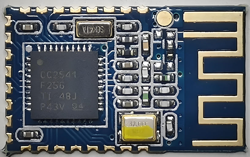
RF boards, or radio frequency printed circuit boards. RF boards are designed to operate with high-frequency signals, typically within the range of 3 kHz to 300 GHz. This capability makes them a critical component in devices that rely on wireless communication, such as mobile phones, satellite systems, and radar equipment.
Unlike regular FR4 PCBs, RF boards are optimized to handle electromagnetic waves in the radio frequency range. They use specialized materials and designs to minimize signal loss, avoid interference, and maintain stable operation. Their importance continues to grow with advancements in wireless technologies, the Internet of Things (IoT), and 5G networks.
The design and manufacturing of RF boards demand meticulous attention to detail, as even minor issues can significantly impact their performance. These boards are vital for applications where precision and reliability are non-negotiable.
Advantages of RF Boards
High-frequency systems require consistent and stable signal transmission. RF boards are designed to reduce signal distortion and ensure accuracy, even in complex environments.
The specialized materials used in RF boards, such as PTFE and Rogers laminates, have low dielectric constants.
RF boards are built to handle heat efficiently.
RF boards can be tailored to meet specific requirements, including frequency range, size, and power capacity.
With RF boards, engineers can integrate cutting-edge technologies like 5G, IoT, and advanced radar systems.
RF boards design ensures long-term reliability, even under challenging conditions.
What Is the Difference Between RF PCB and Normal PCB?
While standard PCBs and RF PCBs may appear similar at first glance, their functions, materials, and design considerations set them apart.
Frequency Handling
Standard PCBs are designed for low to medium frequencies and do not require the precision needed for high-frequency signals. RF PCBs, on the other hand, are built to handle frequencies ranging from kilohertz to gigahertz.
Material Properties
Materials are a defining factor. Normal PCBs commonly use FR-4, a cost-effective and versatile material. In contrast, RF boards use materials like PTFE, Rogers laminates, or ceramic substrates. These materials have low dielectric constants and low loss tangents, ensuring minimal signal degradation.
Signal Integrity
RF boards are engineered to minimize crosstalk and interference. Design considerations include impedance matching and controlled trace dimensions, which are not as critical in standard PCBs.
Application Areas
While standard PCBs are widely used in consumer electronics, RF PCBs find their place in specialized fields like telecommunications, aerospace, and medical devices, where high-frequency signals are essential.
Which Material Is Commonly Used for RF PCBs?
Material selection is critical when designing RF boards. The right material ensures that the board can handle high-frequency signals with minimal loss and distortion.
PTFE (Polytetrafluoroethylene)
PTFE is a common choice for RF PCBs due to its excellent electrical properties. It has a low dielectric constant, which supports stable signal propagation. PTFE is also resistant to heat, making it suitable for high-power applications.
Rogers Laminates
Rogers laminates are widely used in RF designs. These materials offer exceptional thermal stability and low loss tangents, ensuring reliable performance. They are also easy to process, making them a favorite among manufacturers.
Ceramic-Filled Substrates
For applications requiring high power and thermal management, ceramic-filled substrates are an excellent option.
Liquid Crystal Polymer (LCP)
LCP is a flexible, lightweight material suitable for RF boards used in compact devices like smartphones and wearables.
Hybrid Materials
Some RF PCBs combine multiple materials to balance cost, performance, and manufacturability. Hybrid materials allow designers to meet specific application requirements effectively.
What Are RF Circuits Used For?
Telecommunication Systems – RF circuits are the backbone of mobile networks, Wi-Fi routers, and wireless communication devices.
Aerospace and Defense – Radar systems, satellite communication, and military-grade navigation rely on RF circuits.
IoT Devices – The Internet of Things depends heavily on RF circuits for connectivity. From smart home systems to industrial sensors, these circuits enable real-time data exchange.
Medical Equipment – In healthcare, RF circuits support technologies like MRI machines and wireless patient monitoring systems.
Automotive Applications – RF circuits play a key role in modern vehicles, powering advanced driver-assistance systems (ADAS), vehicle-to-everything (V2X) communication, and keyless entry systems.
RF PCB Design Guidelines
Designing RF PCBs can be as challenging as addressing electromagnetic interference (EMI). Success often requires careful planning and attention to the following aspects:
1. Transmission Lines
Select the correct transmission line type (microstrip or stripline) based on the required 50Ω characteristic impedance.
Use impedance calculation tools to design consistent impedance lines and determine appropriate line width and spacing.
Ensure continuity in RF transmission lines by maintaining uniform widths and spacing.
Avoid abrupt transitions or splits in RF signal paths as they impact impedance.
Provide a clean ground reference under the transmission line without interference from other signals.
Minimize transmission line lengths to reduce signal loss, and use wider traces for power lines.
Use compensated bends for corners, avoiding sharp angles.
Avoid forks, stubs, or parallel placement of other lines near RF transmission lines.
Refrain from placing test points directly on RF transmission lines.
2. PCB Layer Stacking
A recommended four-layer stackup for RF PCBs includes:
Top Layer: RF ICs, components, transmission lines, decoupling capacitors, and antennas.
Layer 2: Ground plane.
Layer 3: Power plane.
Bottom Layer: Non-RF components and signal traces.
Ensure a complete and continuous ground plane for RF signal integrity.
Follow the “20H rule,” where the power plane edges are recessed by at least 20 times the plane-to-plane spacing to reduce EMI.
3. Power Decoupling
Place decoupling capacitors as close to power pins as possible.
Use a combination of large and small capacitors for filtering different noise frequencies.
Keep decoupling capacitors and power layers on the same plane, prioritizing smaller values near IC pins.
Avoid vias between decoupling capacitors and IC power pins.
Each decoupling capacitor should have a dedicated ground via.
4. Vias
Use multiple vias to connect layers, spaced no greater than λ/20.
Place ground vias near signal vias to minimize parasitics.
Avoid sharing vias between solder pads and signal traces.
Prefer smaller vias for reduced parasitic effects but balance against manufacturing costs.
Employ ground vias around sensitive components to enhance EMC shielding.
5. Capacitors
Use C0G/NP0 capacitors for temperature stability and frequency consistency.
For decoupling, select capacitors with self-resonant frequencies (SRF) near the operational range.
Employ smaller packages (e.g., 0201 or 0402) to minimize parasitic effects.
Choose high-Q capacitors for RF circuits to reduce losses.
6. Inductors
Use high-Q inductors operating below their SRF for matching circuits.
For filtering, select inductors with SRF near the noise frequencies.
Avoid parallel placement of adjacent inductors to prevent coupling.
Wire-wound inductors offer low DC resistance, high Q, and better current handling, while ceramic inductors provide cost efficiency at the expense of lower Q.
At EBest Circuit (Best Technology), we specialize in manufacturing RF boards tailored to your specific needs. With a commitment to quality and innovation, we deliver solutions that meet the highest standards of performance and reliability. Contact us today to discuss how we can support your next project.
For PCB materials, you may have ever heard about many different kinds of materials such as the materials of FR4, Aluminum, Copper base and ceramic base.
But do you know what the duriod 5880 materials is?
Actually duriod 5880 is a kind of materials of the Rogers, it is the materials which is used for high frequency circuit board. RT 5880, which is famous for its low dielectric loss, low moisture absorption, and stable dielectric constant. The PCB made of duriod 5880 can be widely used in airborne and ground-based radar systems, millimeter wave applications, and space satellite transceivers. Different with other kinds materials, the color of the RT 5880 materials is black.
Why this material can be used in such high end field? Let’s see below to know more information.
Excellent dielectric properties: RT/duroid 5870/5880, as a new generation of high-frequency laminate, is made of polytetrafluoroethylene composite material (PTFE). At the same time, glass microfibers are randomly distributed in the material, which provides the greatest strength during the production and application of the circuit board.
High-frequency circuit design has strict requirements on the dielectric constant of the printed circuit board. RT/duroid 5880 has an ultra-low dielectric constant and remains the same in a very wide operating frequency range.
At 10GHz operating frequency, the measured dielectric constant is only 2.33/2.2, which is significantly lower than similar materials on the market. Therefore, from the perspective of performance parameters and production costs, the board is more suitable for high-frequency application design than similar products.
At the same time, under the same standard (f=10GHz), and the dielectric loss of the RT5880 is only 0.0012/0.0009. The extremely low dielectric loss makes it very suitable for high-frequency and the field of wide-band applications which requiring minimal dispersion and low loss.
In addition, the extremely low moisture absorption rate makes it an ideal choice for applications in high humidity environments. The moisture absorption rate of RT/duroid 5880 is only 0.02%, so it can meet the strict requirements of mechanical reliability and electrical stability in the complex microwave structure design, and it is also suitable for applications in high humidity environments.
With the continuous improvement of the operating frequency of high-frequency circuits, the requirements for the dielectric constant and dielectric loss of the circuit board are becoming more and more stringent. The excellent performance of RT/duroid 5880 in these two aspects can significantly improve the design of high-frequency circuits. Definity, improve circuit performance.
Easy to process and install In this high-frequency design, in order to meet the requirements of electromagnetic shielding and compact design, printed circuit boards are often installed in various irregularly shaped cavity structures. Therefore, the PCB board must be designed in different shapes and suitable for production and Installation.
For RT/duroid 5880 laminate, which is easy to cut, trim and good for PCB manufacturing.
At the same time, it can resist all the solutions and chemical agents used in the process of etching and plating through holes, and it has a good performance of the cold and heat resistance.
The composite material RT/duroid 5880 can be covered with a laminated copper foil for some key electrical applications, and brass plates or copper can also be used as required. Usually laminates of the RT/Duriod 5880, it can make double-sided copper clad with thicknesses ranging from 1/2 oz. to 2 oz./ft2 (8.5~70 μm) to meet most custome’s requirements for the thickness of copper foil.
Our company has focus on the PCB fabricationi for more than 15 years, we can make PCB with Rogers PCB with RT/Duriod 5880, as well as RO4003C and RO4350B with different thickness. If you are interesting to know more and your PCB also want to made of RT/Duriod 5880, please feel freely to contact us for more information related.