When it comes to wireless systems—WiFi, Bluetooth, cellular IoT, radar, GPS, or any RF module—the performance of the radio frequency PCB (RF PCB) directly determines signal integrity, radiation efficiency, and product stability. A radio frequency PCB operates in high-frequency environments where small layout changes may shift impedance, weaken gain, or create unwanted noise. Because of this, a radio frequency PCB requires strict engineering rules, carefully selected materials, and a routing method that protects signal quality.
This article explains what an RF PCB is, the characteristics you must consider, the right FR PCB materials, the correct RF PCB routing rules, and a complete RF PCB design guideline you can follow for your next high-frequency design. Hope this guide is helpful and give you a best solution to design your RF PCB.
What Is a Radio Frequency PCB?
A radio frequency PCB, or RF PCB, refers to a board used to transmit and receive signals at high frequencies—from hundreds of megahertz to multiple gigahertz. These boards are widely used in wireless modules, IoT devices, GPS systems, consumer electronics, radar sensors, and communication infrastructure.
Unlike standard FR4 boards, RF PCBs involve dedicated dielectric materials, controlled impedance structures, and strict layout rules to keep signal integrity stable. The entire PCB—from stack-up to routing—must support predictable propagation velocity, stable loss characteristics, and smooth energy flow.
RF PCBs are used in:
- Wireless modules
- GPS receivers
- Sub-GHz transmitters
- 5G communication units
- Radar sensors
- IoT devices
- RF amplifiers and mixers
- Antenna feed circuits
Their performance depends on trace geometry, ground stability, and how cleanly the RF path is designed.
What Is a Radio Frequency PCB?
Characteristics of an RF PCB
RF PCBs typically have the following characteristics:
- Controlled impedance routing for RF signal paths
- Low-loss PCB materials to minimize attenuation
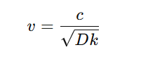
- Stable dielectric constant (Dk) over temperature and frequency
- Strict EMI/EMC requirements
- Short, direct RF trace routing
- Careful grounding strategy (dedicated ground plane, stitching vias)
- Special treatment around matching networks and antenna feeds
Because RF energy behaves like waves rather than simple electrical current, the PCB becomes part of the RF system itself—meaning the layout, stack-up, and materials must be engineered for high-frequency behavior.
What Is the Frequency Range of RF PCB?
RF PCBs typically operate in the following ranges:
| Frequency Band | Range | Typical Applications |
| Low RF | 300 MHz – 1 GHz | ISM band, sub-GHz transmitters |
| Mid RF | 1 GHz – 6 GHz | Wi-Fi, Bluetooth, GPS |
| High RF | 6 GHz – 30 GHz | 5G, radar |
| Millimeter Wave | 30 GHz – 80 GHz | Automotive radar, high-speed links |
Most IoT devices today (BLE, WiFi, Zigbee, Sub-GHz RF) fall between 433 MHz – 6 GHz.
What Is the Best PCB Material for RF?
Choosing the right laminate affects signal quality, trace accuracy, and overall loss.
- FR4 PCB Material
FR PCB material, typically FR4, works for low-frequency RF designs below 2.4 GHz. It offers low cost and good mechanical strength. However, its dielectric properties vary with temperature and frequency. Loss tangent is higher than PTFE, so it works best for short RF paths or low-power consumer wireless modules.
- Rogers RF Materials
Rogers laminates such as RO4350B, RO4003C, and RO5880 are widely used for RF designs due to:
- Low loss tangent
- Very stable dielectric constant
- Smooth copper surface
- High processing consistency
These materials are ideal for GPS, radar, Wi-Fi 6, UWB, sub-6G, and millimeter-wave applications.
- PTFE / Teflon Laminates
PTFE offers excellent RF performance, especially for microwave and radar. It has very low loss and highly stable characteristics. Fabrication needs tight process control due to soft substrate behavior.
- Ceramic Substrates
Ceramics substrate provide strong thermal stability and high dielectric precision. They work well in high-power RF amplifiers, satellite communication modules, and advanced radar systems.
Here is a common radio frequency PCB material table:
| Substrate | Tg (°C) | Td (°C) | Dk | Loss Tangent | Band |
| FR4 | ~135 | ~295 | < 4.4 | ~0.022 (parasitic ignored) | X–K |
| Isola MT40 | 200 | 360 | 3.38–3.75 | 0.0028–0.0035 | W |
| IS680 AG-348 | 200 | 360 | 3.48 | 0.0029 | W |
| IS680 AG | 200 | 360 | 3.00–3.48 | 0.0020–0.0029 | W |
| IS680 | 200 | 360 | 2.80–3.45 | 0.0025–0.0035 | W |
| Isola MT77 | 200 | 360 | 3.00 | 0.0017 | W |
| Rogers 3003 | NR | 500 | 3.00 | 0.0013 | W |
| Rogers 3006 | NR | 500 | 6.15 | 0.0022 | X–Ka |
| Rogers 4360 | >280 | 407 | 6.15 | 0.0038 | X–Ka |
| RT Duroid 6010.2LM | NR | 500 | 10.70 | 0.0023 | X–Ka |
| RT Duroid 6202 | NR | 500 | 2.90 | 0.0015 | X–Ka |
| RT Duroid 6006 | NR | 500 | 6.45 | 0.0027 | X–Ka |
| RT Duroid 6035 | NR | NR | 3.50 | 0.0013 | X–Ka |
(Note: NR means Not Reported)
PCB Design Guide for Radio Frequency RF Boards
Designing RF PCBs involves stack-up planning, controlled impedance, grounding, spacing, matching networks, and EMI reduction. Below are the recommended RF PCB guidelines and routing rules you can apply to achieve stable wireless performance.
1. Start With Complete RF Design Information
Successful RF PCB design begins long before the first trace is drawn. Engineers must collect all essential RF parameters to avoid redesigns later. This includes:
- Functional description and operating frequency band
- Current and voltage requirements of each RF stage
- RF component list and package dimensions
- PA gain, receiver sensitivity, and system isolation targets
- Planned PCB stack-up structure
- Controlled impedance values
- Mechanical constraints and enclosure limits
- Shielding frame or metal-can dimensions
- Matching network reference designs
- Simulation results for power amplifiers and LNAs
Gathering this information early ensures that layout decisions align with system-level RF performance.
PCB Design Guide for Radio Frequency RF Boards
2. Physical Zoning of the RF PCB
Physical zoning organizes the board according to how RF signals flow.
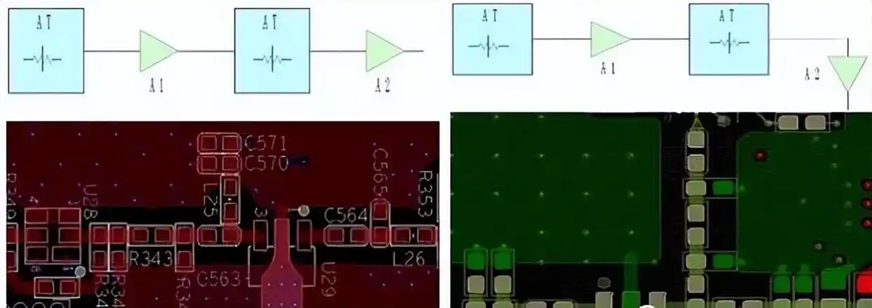
- RF Signal Flow Placement
Place RF components in the exact order of the signal chain. A short, direct, and linear path minimizes insertion loss, improves impedance stability, and preserves gain.
- RF Component Orientation
Rotate filters, PAs, LNAs, couplers, and mixers so their input/output pins align with the straightest possible RF path. Avoid unnecessary detours or bends.
- Isolation Through Ground Structures
To prevent RF coupling and cross-interference, isolate RF sections using:
- Ground shielding walls
- Via-fence structures
- Shield cans over sensitive circuits
- Copper barriers or partitions
These structures keep RF and digital noise apart, improving overall stability.
3. Electrical Zoning
Electrical zoning separates different circuit domains so they cannot interfere with each other.
- Power section: Power management ICs, regulators
- Digital control section: MCUs, logic circuits, clocks
- Analog RF section: LNAs, PAs, filters, mixers, antennas
These zones should not overlap in routing. Digital switching noise or PLL jitter can easily couple into RF paths if the layout is not properly divided.
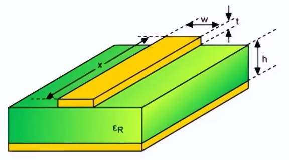
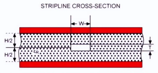
4. RF Transmission Line Structures
RF PCBs commonly use one of three controlled-impedance transmission line types:
Microstrip Line
- RF trace on the top layer
- Continuous ground plane directly beneath (Layer 2)
- Impedance determined by trace width and dielectric height
- Ideal for simple and low-to-mid–frequency RF designs.
Stripline
- RF trace routed on an inner layer
- Sandwiched between two solid ground planes
- Provides superior isolation and uniform impedance
- Useful in compact or high-frequency designs where shielding is critical.
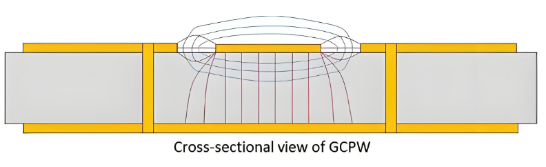
Grounded Coplanar Waveguide (GCPW)
- Top-layer trace with ground on both sides
- Ground plane below the trace
- Excellent isolation and impedance control
- Often preferred when space is tight or when multiple RF lines run in parallel.
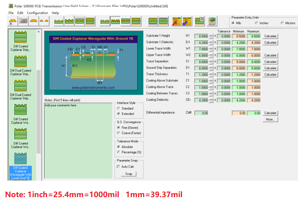
5. Impedance Selection and Calculation
Achieving the correct characteristic impedance (typically 50Ω) requires considering:
- Trace width
- Copper thickness
- Dielectric constant (Dk)
- Dielectric height between layers
Use tools such as Polar SI9000 or your PCB manufacturer’s impedance calculator.
6. RF Trace Bending Rules
Straight RF traces are ideal, but bends are sometimes unavoidable.
Follow these rules:
- Minimum bend radius ≥ 3× trace width
- Avoid 90° bends (cause impedance discontinuity)
- Use 45° bends or smooth arc/bowed shapes
- Apply mitering to compensate for impedance changes
For critical RF links, simulate bends in an EM solver to validate performance.
7. Layer Transitions for RF Traces
RF traces should stay on one layer. If a layer change is unavoidable:
- Use two vias at minimum
- Via diameter should match the RF trace width
- When space is tight, use three smaller vias in parallel
Multiple vias reduce via inductance and minimize impedance mismatch.
8. Signal Isolation Rules
Isolation is as important as impedance control in RF design.
a) RF Lines
- Keep RF traces well separated
- Avoid long parallel runs
- Use GCPW for noisy or densely packed areas
- Keep sensitive microwave lines away from high-power circuits
b) High-Speed Digital Signals
- Route digital clocks on different layers
- Avoid crossing beneath RF paths
- Switching noise can modulate RF signals if not isolated
c) Power Lines
- Use a dedicated power layer for stable distribution
- Place bypass capacitors close to RF IC power pins
- Keep power traces away from RF transmission lines
9. Ground Area Design
Ground integrity determines the quality of RF performance.
- Use solid, continuous ground planes
- Avoid slots, gaps, and return-path interruptions
- Do not route signals across RF ground regions
- Add abundant ground stitching vias
- Reduce inductance in ground loops
In RF PCB design, a 4-layer RF PCB design is widely considered the most balanced structure for modern wireless modules because it provides stable impedance, strong isolation, and efficient routing without dramatically increasing manufacturing cost. While 2-layer boards are cheaper and 6-layer boards offer more routing space, the 4-layer stack-up delivers the best performance-to-cost ratio for most RF applications under 6 GHz.
Below is the recommended stack up:
- Layer 1 (Top Layer): RF traces + components
- Layer 2 (Ground Plane): Continuous ground reference
- Layer 3 (Power Plane): Power routing + local shielding below RF areas
- Layer 4 (Bottom Layer): Non-critical routing or power distribution
RF PCB Routing Rules You Must Follow
1. The length of the RF traces should be kept as short as possible, and ensure that the surrounding densely arranged holes are shielded. The intervals should be approximately 50 mils.
2. RF traces must not have vias, meaning they cannot cross layers. It is preferable to use 135° angle traces or circular traces.
3. Near the RF traces, there should be no high-frequency signal lines. Pay attention to the UART signal line being shielded by a ground layer, and add ground holes around it for protection.
4. The RF traces should be as close as possible to the size of the pads.
5. For the RF traces, matching networks and the area around the antenna socket > 0.8mm, copper cannot be laid; they need to be hollowed out.
6. The RF traces should be kept as far away from the battery holder as possible, with a distance of at least 5mm or more.
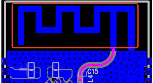
7. A π-type matching circuit needs to be reserved on the RF path, and this π-type matching circuit should be placed close to the chip end like below diagram show:
IPC Standards for Radio Frequency PCB
The following IPC standards are typically referenced for RF PCB and high-frequency designs:
- IPC-6018 – Qualification and Performance Specification for High Frequency (Microwave) PCBs
- IPC-2221/2222 – General & rigid PCB design rules
- IPC-2141 – Controlled impedance design
- IPC-TM-650 – Test methods for dielectric materials
- IPC-4103 – High-frequency base materials
These standards help ensure reliability, board performance, and manufacturability for RF and microwave applications.
Your Reliable RF PCB Manufacturer – EBest Circuit (Best Technology)
Best technology is an experienced RF PCB manufacturer in China, we offer stack-up consultation, material selection, transmission line simulation, and impedance guidance for complex RF modules. Our production lines use SI9000 modeling, fine etching control, and well-controlled lamination parameters. Our radio frequency PCB manufacture capability including:
- Rogers, SY, Isola, PTFE, and hybrid RF PCB materials
- Tight-tolerance controlled impedance
- 4–10 layer high-frequency stack-ups
- Laser drilling, buried/blind vias
- Ceramic-filled dielectric PCB options
- Full DFM & design support for RF modules and antennas
In addition to this, we offer one-stop PCB & PCBA service covers RF tuning, antenna matching, shielding assembly, coaxial connector installation and final functional RF tests.
Whether you’re building Bluetooth modules, RF front ends, radar circuitry, or custom antennas, our engineering team ensures high yield and reliable RF performance—helping you bring your wireless product to market faster.
FAQs about RF PCBs
1. What materials are recommended for radio frequency PCB?
Rogers RO4350B, RO4003C, RO5880, PTFE, and high-stability ceramics work best for RF or microwave applications.
2. Can I use FR4 for RF PCB?
Yes, if the operating frequency is low and the RF path is short. Many 433 MHz and 2.4 GHz consumer modules still use FR4.
3. Why should RF traces avoid vias?
A via adds inductance and disrupts impedance. RF energy prefers a continuous layer.
4. What routing structure is most common?
Microstrip and grounded coplanar waveguide are widely used due to predictable impedance.
5. Does EBest Circuit (Best Technology) support RF PCBA assembly?
Yes, including antenna tuning, shielding, coaxial connector mounting, and final RF testing.