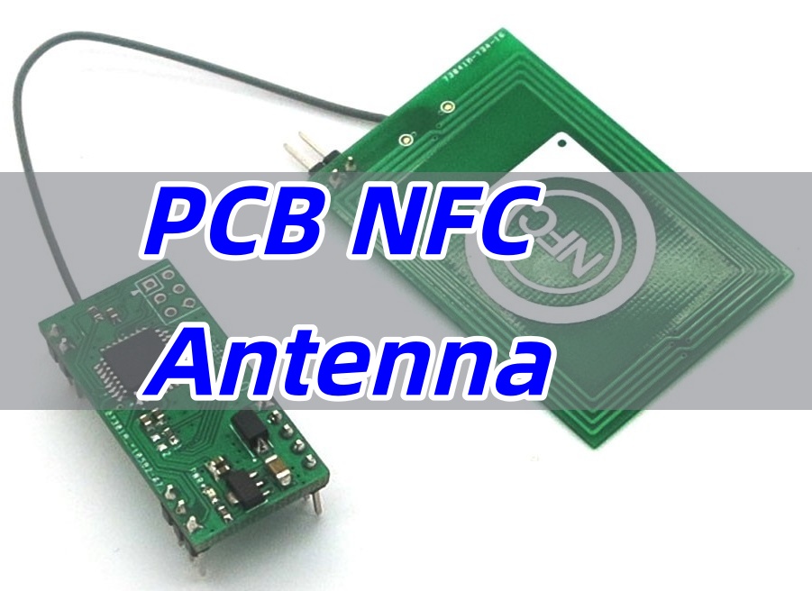
PCB NFC antenna enables seamless near-field communication in smartphones, payment systems, and IoT devices. This article explores their design, differences from RFID antennas, and practical applications.
Why do many struggle with NFC antenna integration? Here are common challenges:
- Complex impedance matching – Achieving optimal performance at 13.56MHz is tricky.
- Size constraints – Balancing compact designs with adequate inductance (typically <5μH).
- Material selection – FR4, flex PCB, or ceramic substrates impact efficiency.
- Interference issues – Nearby metal components can disrupt magnetic coupling.
- Manufacturing precision – Tight tolerances for trace width/spacing (e.g., 0.2mm±0.02mm).
EBest Circuit (Best Technology) solves these with the following proper solutions:
- Impedance tuning tools – HFSS simulations and network analyzer validation.
- Miniaturization expertise – Down to 0.15mm thin PCBs with 20oz heavy copper.
- Material guidance – Recommending optimal substrates (Aluminum, Rogers, or LTCC).
- Shielding solutions – Ground planes and ferrite layers to reduce interference.
- High-precision production – 260,000 ft²/month capacity with ±1mil tolerance.
BEST Technology is an industry-leading PCB manufacturer with 19 years of expertise in advanced circuit solutions, specializing in high-performance PCB NFC antenna designs and innovative flexible circuit applications. As a trusted partner in RF and wireless technologies, we combine precision engineering with cutting-edge manufacturing to deliver optimized NFC antenna PCBs that meet stringent performance requirements.
Our ISO-certified facility supports end-to-end production from rapid prototyping to mass manufacturing, with specialized capabilities in impedance-controlled designs and multi-layer NFC antenna PCB integration. With a 97% on-time delivery rate and dedicated engineering support, we provide tailored solutions for IoT, smart devices, and contactless systems requiring reliable PCB-based NFC antennas. For customized NFC antenna PCB solutions, pls feel free to contact our technical sales team at sales@bestpcbs.com.
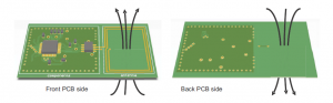
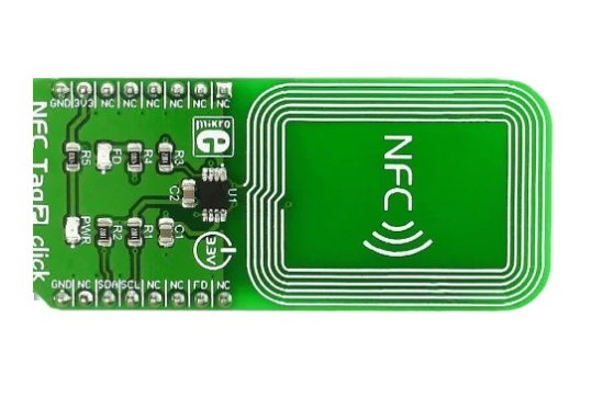
What Is a PCB NFC Antenna?
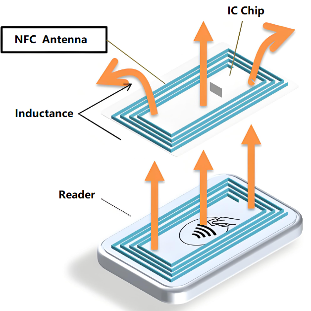
A PCB NFC antenna is a printed circuit board coil enabling 13.56MHz communication within 10cm. It works via magnetic induction, transferring energy and data between devices.
Key features:
- Inductance range: 1–5μH for stable resonance.
- Layers: Single-sided (cost-effective) or double-sided (higher inductance).
- Materials: FR4 (standard), flexible PCBs (wearables), or ceramic (high-temperature).
What are the NFC Antenna Types?
Near Field Communication (NFC) antennas are essential components in contactless applications, enabling secure data transfer and wireless power transfer. The design of an NFC antenna significantly impacts performance, influencing factors such as read range, efficiency, and compatibility with different devices. Below are three common NFC antenna types, each with distinct advantages for specific applications:
- Rectangular Spiral – Simple to design and cost-effective, making it ideal for standard FR4 PCBs in access control and identification systems.
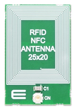
- Circular Spiral – Generates a more uniform magnetic field, preferred for payment terminals and industrial applications requiring consistent performance.
- Double-Layer Helix – Maximizes inductance in tight spaces, commonly used in smartphones and wearables where miniaturization is critical.
EBest Circuit (Best Technology)’s NFC antenna design tool helps select the right type based on your device’s size and frequency requirements.
What is Difference: PCB NFC Antenna v.s. PCB RFID Antenna
While both NFC (Near Field Communication) and RFID (Radio Frequency Identification) antennas enable wireless communication, they serve distinct purposes in PCB applications. The key differences lie in their operating frequencies, communication ranges, and typical use cases. Below is a comparative breakdown:
| Feature | PCB NFC Antenna | PCB RFID Antenna |
|---|---|---|
| Frequency | 13.56 MHz (fixed) | 125 kHz – 2.45 GHz (varies by type) |
| Range | Short-range (<10 cm) | Medium- to long-range (up to 15 m) |
| Applications | Mobile payments, device pairing, smart tags | Inventory tracking, access control, logistics |
Design Considerations:
- NFC Antennas: Optimized for close-proximity interactions, requiring precise impedance matching and compact spiral/helix layouts (e.g., circular spirals for uniform fields).
- RFID Antennas: Designed for broader frequency adaptability, often using dipole or loop configurations for extended range.
Key Takeaways:
- NFC antennas prioritize proximity and security, while RFID antennas focus on scalability and range.
- Frequency selection dictates antenna geometry—spiral for NFC, dipole/loop for RFID.
- Our engineering team provides application-specific guidance for optimal performance.
EBest Circuit (Best Technology) offers tailored design tools for both technologies, including an NFC antenna optimizer for 13.56 MHz tuning and an RFID antenna calculator for UHF/HF band trace patterns. For custom antenna designs, prototypes, fabrication, assembly, or box build, pls contact us at sales@bestpcbs.com.
How is NFC Antenna Size?
The size of an NFC antenna is a critical design parameter that directly impacts its performance, efficiency, and suitability for specific applications. Proper sizing ensures optimal inductance, read range, and compatibility with device constraints. Below, we break down the key considerations for NFC antenna sizing, supported by technical guidelines and empirical data.
1. Size Guidelines for Common Applications
NFC antenna dimensions vary based on device type and functional requirements:
- Smartphones:
- Recommended size: 25×15mm
- Design: 5 turns with 0.3mm trace width to balance inductance (~1–2 µH) and space efficiency.
- Rationale: Larger coils enhance magnetic coupling but must fit within compact device layouts.
- Wearables:
- Recommended size: 15×10mm (flexible PCB compatible)
- Design: 3 turns to maintain adequate inductance (~0.5–1 µH) while minimizing footprint.
- Rationale: Smaller form factors require trade-offs between turns and trace width to avoid excessive resistance.
2. Key Factors Influencing Antenna Size
a. Inductance (L) Requirements
The antenna’s inductance must match the NFC chip’s tuning capacitance (typically 27–33 pF for 13.56 MHz). Use the simplified formula for spiral coil inductance:
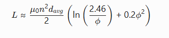
Where:
- μ0: Permeability of free space (4π×10−7 H/m)
- n: Number of turns
- davg: Average coil diameter
- ϕ: Fill factor (trace width/spacing ratio).
Example: A 25×15mm antenna with 5 turns yields ~1.5 µH, suitable for most NFC ICs.
b. Trace Width and Spacing
- Narrow traces (0.2–0.3mm): Reduce parasitic capacitance but increase resistance.
- Wider traces (>0.5mm): Lower resistance but risk eddy currents and size inflation.
c. Device Integration Constraints
- Ground plane proximity: Keep >1mm clearance beneath coils to avoid Q-factor degradation.
- Bending radius (flex PCBs): Minimum 3× trace width to prevent cracking.
3. Layout Optimization Techniques
- Avoid 90° corners: Use 45° miters to minimize impedance discontinuities and EMI.
- Parallel trace alignment: Maintain ±5° skew tolerance for uniform current distribution.
- Symmetry: Ensure balanced coil geometry to prevent field distortion.
NFC antenna sizing is a trade-off between electrical performance (inductance, Q-factor) and physical constraints (device size, integration).
Designers must:
- Match inductance to the NFC chip’s requirements using empirical formulas.
- Optimize trace geometry for minimal resistance and EMI.
- Validate prototypes with network analyzers to ensure resonant frequency alignment.
Key Takeaways:
- Smartphones: 25×15mm (5 turns) balances performance and space.
- Wearables: 15×10mm (3 turns) prioritizes miniaturization.
- Layout precision (trace width, symmetry) is as critical as size.
For tailored NFC antenna solutions, consult EBest Circuit (Best Technology)’s engineering team at sales@bestpcbs.com.
How is the NFC Antenna PCB Layout?
The layout of an NFC antenna on a PCB is crucial for achieving optimal performance in wireless communication systems. A well-designed NFC antenna PCB ensures efficient energy transfer, minimal interference, and reliable operation. This section explores key considerations and best practices for NFC antenna PCB layout, supported by technical insights and empirical data.
1. Ground Plane Management
Proper ground plane design is essential to prevent performance degradation in NFC antennas:
- Avoid Ground Planes Under Coils:
Placing ground planes directly beneath the antenna coils can induce eddy currents, which weaken the magnetic field and reduce read range. Maintain a clearance of at least 1mm between the coil and any ground layer. - Use Split Ground Planes:
For multilayer PCBs, consider splitting the ground plane around the antenna area to minimize parasitic capacitance and maintain a high quality factor (Q).
2. Trace Design and Geometry
The geometry of the antenna traces significantly impacts performance:
- Trace Width and Spacing:
- Width: 0.2–0.5mm (balance between resistance and parasitic capacitance).
- Spacing: ≥0.2mm to avoid arcing and ensure manufacturability.
- Corner Design:
- Use 45° miters instead of 90° bends to reduce electromagnetic interference (EMI) and impedance mismatches.
- The inductance of a corner can be approximated by: L corner≈0.2×L straight
- Where L straight is the inductance of a straight trace segment.
- Parallel Traces:
Maintain alignment within ±5° skew to ensure uniform current distribution and consistent inductance.
3. Antenna Symmetry and Balance
A symmetrical layout is critical for generating a uniform magnetic field:
- Differential Feed Design:
For balanced NFC antennas, ensure equal trace lengths and impedance matching (±10% tolerance) between differential pairs to prevent signal distortion. - Coil Shape:
- Circular spirals provide the most uniform field distribution but require precise manufacturing.
- Rectangular spirals are easier to fabricate but may exhibit slight field asymmetry.
4. Material and Layer Stackup
The choice of PCB materials and layer configuration affects antenna performance:
- Substrate Material:
- FR4: Cost-effective but with higher dielectric losses (~0.02 at 13.56 MHz).
- Polyimide (Flex PCBs): Lower loss tangent (~0.005) and better for bendable designs.
- Layer Stackup:
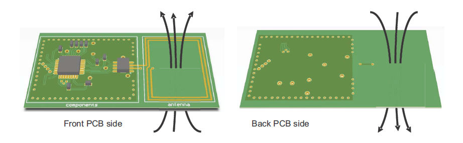
- 2-Layer PCBs: Place the antenna on the top layer with a partial ground plane underneath.
- 4-Layer PCBs: Use Layer 2 as a ground reference and avoid routing critical signals near the antenna area.
5. EMI and Crosstalk Mitigation
To minimize interference:
- Shielding:
Add a Faraday cage or conductive tape around the antenna if nearby components emit noise. - Isolation:
Keep high-speed digital traces (e.g., USB, HDMI) **≥10mm** away from the antenna to prevent coupling.
In conclusion, an optimized NFC antenna PCB layout requires:
- Strategic ground plane design to avoid eddy currents.
- Precise trace geometry (width, spacing, corners) for consistent inductance.
- Symmetrical coil patterns to ensure uniform magnetic fields.
- Material selection tailored to application needs (rigid vs. flex PCBs).
- EMI mitigation through shielding and isolation.
For performance-critical applications, prototype testing with a network analyzer is recommended to validate resonant frequency and Q-factor.
Key Takeaways:
- Ground plane clearance ≥1mm prevents field degradation.
- 45° corners and parallel traces enhance signal integrity.
- Differential feed designs improve balance in high-performance systems.
How to Design a PCB NFC Antenna?
NFC (Near Field Communication) is a short-range wireless communication technology operating at 13.56 MHz, designed for secure communication within a few centimeters. NFC antennas are essential components in mobile devices, contactless payments, and access control systems. Designing a PCB NFC antenna requires understanding both antenna theory and practical PCB layout considerations to achieve optimal performance, compact size, and reliable communication.
Key Antenna Parameters and NFC Working Principle
The performance of an NFC system depends heavily on the antenna, which determines parameters such as input impedance, efficiency, gain, polarization, and inductive coupling.
- Input Impedance
Input impedance is the ratio of voltage to current at the antenna terminals:Zin = V / IIt consists of a real part (radiation and loss resistance) and an imaginary part (reactive energy storage). Return loss describes matching:RL = -20 * log10(|Γ|)where Γ is the reflection coefficient. For mobile NFC antennas, a return loss of -5 dB or lower is generally acceptable. - Antenna Efficiency
Efficiency is the ratio of radiated power to input power:ηA = Prad / PinLosses may include conductor resistance, dielectric loss, and reflection from impedance mismatch. - Gain and Directivity
Gain (G) relates to directivity (D) and efficiency:G = ηA * DMobile antennas are usually omnidirectional to avoid blind spots. - Polarization and Inductive Field
NFC antennas typically use linear polarization. The reactive near-field region of the antenna, important for NFC coupling, is approximately:r < D^2 / λwhere D is the largest antenna dimension, and λ is the wavelength. - NFC Communication Modes
NFC supports active and passive modes for peer-to-peer and card-reader communication, typically at 106, 212, or 424 kbps.
Steps to Design a PCB NFC Antenna
1. Select the Antenna Type
Common PCB NFC antenna types include:
- Single-sided rectangular coil
- Single-sided rounded rectangular coil
- Double-sided helical coil
Design choice depends on:
- Available PCB space
- Required inductance
- Miniaturization needs
2. Calculate Key Parameters
Inductance Calculation:
For a coil antenna, the inductance L is:
L = Im(Z) / (2 * π * f)
where Im(Z) is the imaginary part of impedance, and f is frequency (13.56 MHz for NFC). The resonant frequency of the LC circuit is:
f = 1 / (2 * π * √(L * C))
The inductance should generally be below 5 μH for ease of impedance matching with capacitors.
3. Design the PCB Layout
- Determine line width (w), spacing (s), and number of turns (n).
- Keep coil area maximized while maintaining spacing for manufacturability.
- Avoid placing metal components under or near the coil, as they reduce coupling.
- For multilayer boards, consider double-sided or stacked coil designs to increase inductance without enlarging footprint.
4. Impedance Matching
Impedance matching minimizes return loss and maximizes power transfer:
- Connect a series or parallel capacitor to tune resonance.
- Optional: add a resistor for fine adjustment of Q factor.
- Iteratively simulate and measure until return loss is acceptable at 13.56 MHz.
5. Simulation and Verification
- Use electromagnetic simulation tools (e.g., HFSS) to model the antenna and optimize parameters.
- Practical testing with a network analyzer can validate impedance, inductance, and return loss.
- Adjust coil turns, spacing, or matching components if necessary.
6. Miniaturization Techniques
- Use rounded or spiral coil shapes to save PCB space.
- Consider multi-turn or double-sided coils to maintain inductance in a smaller area.
- Optimize trace width and spacing to maintain inductance while minimizing PCB area.
Comparison of Common Antenna Types
| Antenna Type | Size | Inductance Stability | Integration Ease |
|---|---|---|---|
| Single-sided rounded rectangle | Compact | High | Easy |
| Double-sided rectangular | Larger | Moderate | Medium |
| Double-sided helical | Moderate | Good | Medium |
For mobile devices, the single-sided rounded rectangular antenna often offers the best balance between size, stability, and manufacturability.
Practical Design Tips
- Keep the coil away from metal objects and noisy signals.
- Use appropriate PCB material for low-loss high-frequency performance.
- Adjust trace width and spacing to fine-tune inductance.
- Verify resonance and matching through both simulation and measurement.
- When reducing antenna size, consider multi-layer designs and coil shape optimization.
In a nutshell, designing a PCB NFC antenna requires careful consideration of antenna type, inductance calculation, PCB layout, and impedance matching. By following the steps above and applying miniaturization techniques, designers can achieve efficient, compact NFC antennas suitable for mobile devices and contactless systems. Simulation tools and practical validation ensure reliable performance at 13.56 MHz. Among common designs, the single-sided rounded rectangular antenna generally offers the best combination of stability, size, and ease of integration.
What are the Applications of NFC Antenna PCB?
The NFC antenna PCB is a quiet workhorse in our daily tech. You might not see it, but it’s everywhere. Its applications are vast and growing quickly. This tiny coil on a board makes countless interactions seamless. Let’s look at some of the most common places you’ll find it.
- Contactless Payment Systems: This is probably the most familiar use. The credit card in your wallet and the terminal at your favorite coffee shop both rely on a PCB NFC antenna. It makes transactions fast, secure, and simple.
- Smartphones: Modern life runs on phones. Every NFC antenna android and NFC antenna iphone has one embedded inside. It enables mobile payments like Google Pay and Apple Pay. It also handles quick pairing with other gadgets.
- Access Control: Forget fumbling with keys. Many offices, hotels, and secure buildings now use NFC keycards. You just tap your card on the reader. The PCB NFC antenna inside the card communicates with the reader to grant access.
- Asset Tracking: Businesses need to manage their inventory efficiently. NFC tags with a PCB RFID antenna are attached to items in a warehouse or books in a library. A quick scan with a reader updates the system instantly. It saves time and reduces errors.
- Consumer Electronics: This area is exploding. Think about pairing your wireless speakers or headphones. Instead of a complicated Bluetooth search, you just tap your phone to the device. This “pairing by tapping” is powered by an NFC antenna PCB. It’s also common in smart home devices, gaming controllers, and more.
From the payment terminal at a store to the smart speaker in your living room, the NFC antenna PCB is a fundamental enabler of modern convenience. Its ability to provide secure, short-range communication and power has unlocked a world of “tap-and-go” applications. As the Internet of Things continues to expand, we will see these clever little antennas integrated into even more aspects of our lives, making our interactions with technology smoother and more intuitive.
Why Choose EBest Circuit (Best Technology) as Your Reliable NFC Antenna PCB Manufacturer?
Selecting the right manufacturing partner is as critical as the design itself. A perfect design can be ruined by poor fabrication. This is especially true for a sensitive component like a PCB NFC antenna, where precision is paramount. EBest Circuit (Best Technology) stands out as a trusted partner for several key reasons.
With 19 years of dedicated PCB expertise, we have the deep industry knowledge needed to get your NFC antenna PCB right the first time. Our commitment to excellence is clear in what we deliver:
- Certified Quality Systems: We are ISO 9001 and ISO 13485 certified. This means we have robust processes to ensure every board we ship, especially critical ones like a PCB NFC antenna, meets the highest standards of quality and consistency.
- Comprehensive Turnkey Solutions: We offer true end-to-end service. Our support covers everything from initial PCB NFC antenna design review and optimization to full box-build assembly. This simplifies your supply chain and ensures seamless integration.
- Remarkably Fast Lead Times: We understand the need for speed in development. We offer rapid prototyping, with 6-layer FR4 PCB prototypes available in as little as 24 hours. This allows you to test and iterate faster.
- Expert Engineering Support: Our team has deep experience with high-frequency and RF-specific designs. We don’t just build your board; we can help optimize your NFC antenna PCB layout for maximum performance and efficiency, acting as an extension of your engineering team.
- Advanced Manufacturing Capabilities: We use high-quality materials with stable dielectric constants, which is essential for predictable antenna performance. Our controlled manufacturing environment ensures that every NFC PCB antenna we produce performs identically to your prototype, batch after batch.
In closing, choosing EBest Circuit (Best Technology) means more than just finding a supplier; it means gaining a partner dedicated to your success. Our combination of proven quality standards, full-service capabilities, rapid turnaround, and specialized technical support makes us the ideal choice for your NFC antenna PCB needs. We provide the reliability and expertise necessary to transform your innovative designs into high-performing, market-ready products. Let us be the reliable manufacturing foundation that your next great device is built upon.
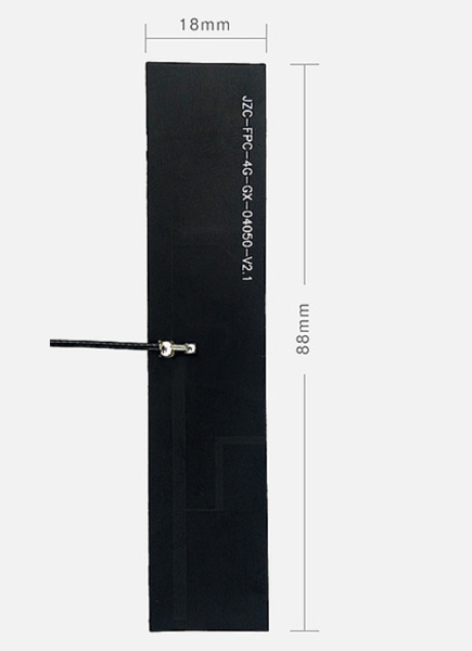
Case of Supporting Embedded PCB NFC Antenna Project at EBest Circuit (Best Technology)
A client needed high-reliability flex PCB NFC antennas for next-generation fitness trackers, with critical challenges:
- Space Constraints: Ultra-compact 12×8mm design area
- Durability Requirements: 100,000+ dynamic bend cycles
Our Solution Leveraged EBest Circuit (Best Technology)’s Advanced Capabilities:
✔ 2-Layer Polyimide Stackup – Optimized with 0.1mm (4mil) traces using our 2/2mil line width/spacing technology
✔ Precision Laser Cutting – Achieved ±0.05mm alignment tolerance (50% tighter than industry standards)
✔ Impedance-Controlled Design – 100% tested to ±5Ω tolerance for 50Ω systems
✔ Medical-Grade Materials – DuPont Pyralux AP polyimide with 260°C/10s solder resistance
✔ Endurance Validation – Exceeded IPC-6013 Class 3 standards for 100k bend cycles
Supported by Our Core Flex PCB Competencies:
◾ 1-30 layer FPC manufacturing ◾ 28,900㎡ monthly capacity
◾ ISO 13485-certified cleanrooms ◾ 98% on-time delivery track record
Result: Delivered 98% on-time with <1% defect rate, enabling seamless integration into mass-produced wearables.
This case highlights how our sub-4mil trace technology, coupled with medical-grade process controls, solves extreme miniaturization challenges while guaranteeing field reliability.
All in all, PCB NFC antennas are vital for secure, short-range communication. Partner with EBest Circuit (Best Technology) for high-performance, cost-effective designs. Pls connect with us sales@bestpcbs.com for any multilayer NFC PCB antenna supports.