What is PCB copper weight? Let’s explores definitions, thickness conversion, current capacity, and selection criteria for PCB copper weight.
Are you troubled with these problems?
Why does my high-density PCB design keep experiencing signal interference?
How do I balance PCB cost and reliability? Low-cost solutions are always unstable!
Small-batch orders have long lead times. How can I quickly verify my design and prototype?
EBest Circuit (Best Technology) can provide services:
- Signal Integrity Optimization: Use simulation tools to predict interference and ensure first-pass EMC testing.
- Cost-Performance Balance: Tiered copper thickness selection (1oz/2oz) saves 20% in material costs.
- 48-Hour Fast Prototyping: Dedicated small-batch production lines prioritize urgent orders.
Welcome to contact us if you have any request for heavy copper PCB: sales@bestpcbs.com.
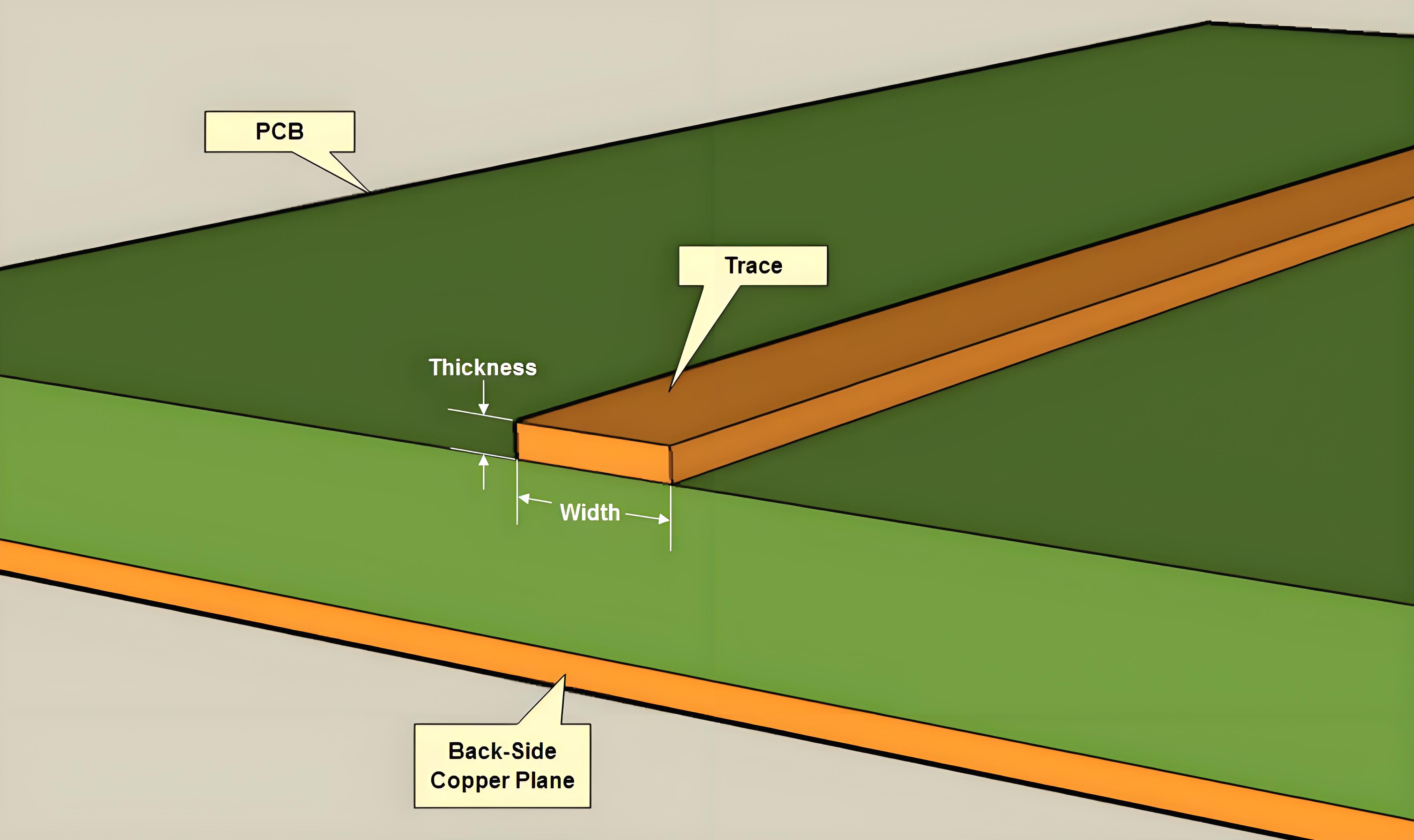
What Is PCB Copper Weight?
PCB Copper Weight refers to the mass of copper per square foot on a printed circuit board, measured in ounces (1 oz = 28.35g). It directly impacts current capacity, heat dissipation, and manufacturing costs, higher oz values (e.g., 2oz, 3oz) mean thicker copper layers for power-heavy designs, while lighter weights (1oz) are common in standard electronics. Engineers choose oz values based on current requirements, thermal needs, and budget constraints, as thicker copper increases cost but improves durability and performance.
What Is PCB Copper Thickness?
PCB Copper Thickness is the physical depth of the copper layer on a circuit board, measured in microns (μm) or mils (1 mil = 0.0254 mm). It defines how much current the trace can carry, its resistance, and thermal performance. Common thicknesses range from 0.5 oz (17.5 μm) for high-frequency designs to 4 oz (140 μm) for high-power applications. Thicker copper improves durability and heat dissipation but increases cost and etching complexity.
Differences Between PCB Copper Weight vs Thickness
| Attributes | Copper Weight | Thickness |
| Definition | Copper mass per unit area (oz/ft² or g/m²) | Vertical height of copper layer (mils or μm) |
| Units | Ounces/square foot (oz/ft²) or grams/square meter (g/m²) | Miles (mils) or microns (μm) |
| Direct Relationship | Increased copper weight→ increased thickness (directly proportional) | Increased thickness → increased copper weight (directly proportional) |
| Conversion Formula | 1 oz/ft² ≈ 34.8 μm (1.378 mils) | Thickness (μm) = Copper Weight (g/m²) / (8.96 × 0.001) |
| Current Capacity Impact | Higher copper weight → higher current carrying capacity | Thicker thickness → higher current carrying capacity |
| Manufacturing Impact | Requires matched laminate thickness and etching precision | Requires controlled etching uniformity to avoid overcut/residue |
| Typical Applications | 0.5 oz/ft² (17.5 μm) → High-density SMT/BGA | 35 μm (1 oz/ft²) → General signal layers |
| 2 oz/ft² (70 μm) → Power planes/high-current | 105 μm (3 oz/ft²) → Industrial control/RF boards |
Copper Weight to Thickness Calculator
Copper Weight to Thickness Conversion
- 1 oz/ft² = 1.37 mils (34.8 μm)
Calculator Formula:
- Thickness (mils) = Copper Weight (oz/ft²) × 1.37
- Thickness (μm) = Copper Weight (oz/ft²) × 34.8
Standard Reference Table
| Copper Weight (oz/ft²) | Thickness (μm) | Thickness (mils) |
| 0.5 | 17.4 | 0.685 |
| 1 | 34.8 | 1.37 |
| 2 | 69.6 | 2.74 |
| 3 | 104.4 | 4.11 |
| 4 | 139.2 | 5.48 |
How to Choose PCB Copper Weight for High Power Applications?
Current Capacity Analysis
- Calculate required trace width based on max current using IPC-2221 formulas or online calculators.
- Select copper weight (1oz=35µm, 2oz=70µm) to match trace width without exceeding temperature rise limits.
Thermal Management Needs
- Use thicker copper (2oz+) for high-power components (e.g., power converters, LED drivers) to enhance heat dissipation.
- Add copper pours or thermal vias under hot components for additional cooling.
Signal Integrity Considerations
- Prioritize thinner copper (0.5oz-1oz) for high-frequency/RF circuits to minimize skin effect losses.
- Avoid excessive copper thickness in impedance-controlled traces.
Cost-Performance Balance
- 1oz copper is standard for most consumer electronics (low cost, adequate for low/mid-power).
- Reserve 2oz+ for industrial/automotive applications requiring robustness.
Manufacturing Constraints
- Confirm PCB fab capabilities: Thicker copper may require specialized processes (e.g., plating, etching).
- Multi-layer boards with heavy copper may increase lead time and cost.
Mechanical Durability
- Use heavier copper for flex/rigid-flex PCBs to improve bend reliability.
- Thicker copper reduces risk of trace fracture under vibration or thermal cycling.
Component Compatibility
- Match pad sizes to copper thickness (e.g., SMT components need consistent solder joints).
- Heavy copper may require larger vias/pads for proper solder wetting.
Environmental Factors
- Choose heavier copper for outdoor/high-humidity environments to resist corrosion.
- Consider ENIG/ENEPIG finishes for heavy copper to enhance solderability.
Relationships Between PCB Copper Weight vs Current
Copper Weight vs. Current Capacity
- Copper weight (oz/ft²) directly determines current-carrying capacity. Thicker copper (e.g., 2 oz/ft² or 3 oz/ft²) supports higher currents due to lower resistance and reduced heat generation.
- Rule of Thumb: 1 oz/ft² copper ≈ 1 A/mm line width (adjust for temperature rise and layer type).
Trace Width Impact
Wider traces reduce resistance and heat, enabling higher current. For example:
- 1 oz/ft² copper, 0.25 mm width ≈ 1.5 A
- 2 oz/ft² copper, 0.25 mm width ≈ 2.5 A
- Use IPC-2221 or IPC-2152 standards for precise calculations.
Temperature Rise Constraints
- Maximum allowable temperature rise (e.g., 10°C or 20°C) dictates copper weight and trace width. Thicker copper mitigates heat buildup in high-current applications.
Application-Specific Recommendations
- Low Current (<1 A): Use 0.5–1 oz/ft² copper with minimal trace width. High Current (>3 A): Opt for 2–6 oz/ft² copper and wider traces (e.g., ≥1 mm).
- Power Distribution: Thick copper (>2 oz/ft²) paired with thermal vias for heat dissipation.
Layer Considerations
- External layers dissipate heat better than internal layers. For internal traces, reduce current capacity by 10–20% or use thicker copper.
Industry Standards & Tools
- IPC-2152: Primary standard for current capacity, accounting for layer type, copper weight, and temperature.
- Saturn PCB Toolkit: Free software for calculating trace/via current capacity based on IPC-2152.
Why Choose EBest Circuit (Best Technology) as PCB Manufacturer?
- 19 Years of PCB Manufacturing Experience: Flexibly handle various problems encountered in PCB production and largely reduce maintenance costs.
- ISO 14001/ISO 13485, ROHS/REACH Certification: medical/automotive customers are exempt from secondary testing, and compliance costs are reduced by 30%
- Strict Quality Inspection: 100% quality inspection for bulk orders to reduce field failures.
- Fast Turnaround (24 hours Rapid Prototyping, 5-7 days Bulk Production): Accelerated timelines without quality compromise.
- Cost-Effective Solutions: Bulk discounts and material optimization reduce PCB costs.
- Free DFM Analysis: Avoid costly redesigns, reduce prototype iterations.
- Competitive Price: Save 15–25% on PCB costs without compromising quality.
- Turnkey Solutions: Full-service PCB manufacturing from design to delivery, accelerating your product’s time-to-market.
Contact EBest Circuit (Best Technology) to unlock cost savings, accelerated timelines, and flawless execution. Whether you need rapid prototypes or high volume production, our team ensures your PCBs meet standards. Get a quote now: sales@bestpcbs.com.