

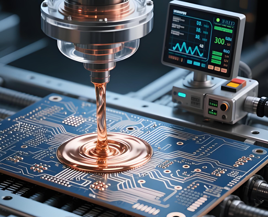
High speed PCB design Radiocord technologies refers to advanced printed circuit board engineering techniques used to ensure stable signal transmission at high data rates and fast edge speeds. This article explains what defines a high-speed PCB, the frequencies that require high-speed design rules, suitable materials like FR4, impedance control requirements, stackup strategies, crosstalk mitigation, simulation tools, and practical design workflows.
Modern electronics, from 5G infrastructure and autonomous vehicles to data centers and high-performance computing, depend heavily on high-speed circuit boards. Engineers must carefully manage signal integrity, impedance, electromagnetic interference, and layer structure to maintain performance. Without disciplined design methods, high-speed signals can degrade quickly due to reflections, noise coupling, or timing skew.
Below is a comprehensive guide to understanding and implementing high-speed PCB design principles.
What Is Considered a High Speed PCB?
A high-speed PCB is a printed circuit board designed to transmit digital or RF signals with extremely fast rise times or high operating frequencies while preserving signal integrity.
Unlike conventional PCBs, high-speed boards must account for transmission line behavior. Once signal edges become fast enough, traces no longer behave like simple copper connections; they act like controlled impedance transmission lines.
Typical characteristics of high-speed PCBs include:
- Fast Signal Rise Time: Signals with rise times below about 1 ns generally require high-speed design considerations.
- High Data Rates: Interfaces such as PCIe, USB 3.0, USB4, HDMI, DDR4, DDR5 memory, and 10G Ethernet operate at speeds where routing geometry directly affects signal quality.
- Transmission Line Effects: Trace impedance, reflection control, and termination become essential for maintaining waveform integrity.
- Strict Signal Integrity Requirements: Engineers must manage reflection, jitter, skew, crosstalk, and EMI.
In practice, the definition of high speed often depends more on edge rate than clock frequency.
What Frequency Requires High Speed PCB Design?
High-speed design rules typically apply when signal frequencies exceed 50 MHz to 100 MHz, although the exact threshold varies depending on signal rise time.
Engineers often use the following guideline:
If the trace length exceeds one-sixth of the signal rise distance, the signal must be treated as high-speed.
A simplified estimation formula is:
Distance = Rise Time × Signal Velocity
In FR4 materials, signal velocity is roughly 150 to 180 mm per nanosecond.
For example:
- Rise time = 1 ns
- Signal travel ≈ 150 mm
Therefore, traces longer than about 25 mm require transmission-line analysis.
High-speed PCB design is commonly required for systems operating in:
| Application | Typical Frequency |
|---|---|
| DDR Memory | 800 MHz – 3 GHz |
| USB 3.0 | 5 GHz |
| PCIe Gen4 | 16 GHz |
| RF Communication | 1 GHz – 40 GHz |
As frequencies increase, PCB layout precision becomes critical.
Can FR4 Be Used for High Speed PCB?
Yes, FR4 can be used for many high-speed PCB designs, especially when signal frequencies remain below about 3 GHz to 5 GHz.
FR4 remains widely used because it offers a strong balance of cost, mechanical strength, and manufacturability.
Typical FR4 electrical properties include:
| Parameter | Typical Value |
|---|---|
| Dielectric constant (Dk) | 4.2 – 4.6 |
| Loss tangent (Df) | 0.015 – 0.02 |
| Thermal stability | Good |
| Cost | Low |
However, FR4 has some limitations.
Limitations of FR4 in High-Speed Design
1. Higher signal loss at GHz frequencies
2. Dielectric constant variation with frequency
3. Increased insertion loss for long traces
For extremely high-frequency designs such as RF and millimeter-wave systems, engineers typically select specialized materials such as Rogers RO4350B, PTFE laminates, or Panasonic Megtron series. These materials offer lower dielectric loss and more stable electrical properties.
What Impedance Is Used in High Speed PCB?
Controlled impedance is one of the most important aspects of high-speed PCB design.
Common impedance values include:
| Signal Type | Typical Impedance |
|---|---|
| Single-ended signals | 50 Ω |
| Differential pairs | 100 Ω |
| USB differential | 90 Ω |
| Ethernet differential | 100 Ω |
| PCIe differential | 85 Ω |
Impedance depends on several factors:
- trace width
- dielectric thickness
- copper thickness
- reference plane distance
- dielectric constant
Engineers usually calculate impedance using field solvers or PCB design tools before fabrication.
Accurate impedance ensures minimal signal reflection, stable waveform shape, and reliable high-speed communication.
What Stackup Is Best for High Speed PCB?
The PCB stackup strongly influences signal integrity, EMI performance, and impedance control.
A well-designed stackup provides continuous reference planes, symmetrical structure, and short return current paths.
A common 8-layer high-speed stackup may look like this:
| Layer | Function |
|---|---|
| L1 | High-speed signals |
| L2 | Ground plane |
| L3 | Signals |
| L4 | Power plane |
| L5 | Power plane |
| L6 | Signals |
| L7 | Ground plane |
| L8 | Signals |
Important stackup design principles:
- Place ground planes next to signal layers: This minimizes loop inductance and EMI.
- Use differential pair routing layers: High-speed interfaces benefit from symmetric routing layers.
- Maintain consistent dielectric thickness: This helps ensure controlled impedance.
- Avoid split planes under high-speed traces: Return currents must have a continuous path.
How Do You Reduce Crosstalk in High Speed PCB?
Crosstalk occurs when electromagnetic coupling causes interference between nearby signal traces.
This effect becomes severe in high-speed systems.
Common techniques to reduce crosstalk include:
- Increase Trace Spacing: A typical guideline is trace spacing greater than or equal to 3 times trace width. Greater spacing reduces capacitive coupling.
- Use Ground Guard Traces: Placing grounded traces between signals helps isolate electromagnetic fields.
- Route Differential Pairs Carefully: Maintain constant spacing, matched lengths, and minimal skew.
- Use Solid Ground Planes: Ground planes provide return paths and reduce loop area.
- Avoid Parallel Routing: Long parallel traces increase inductive and capacitive coupling.
Engineers often stagger signal routing to minimize overlap.
What Simulation Tools Are Used for High Speed PCB?
Simulation tools allow engineers to predict signal behavior before manufacturing.
Common high-speed PCB simulation tools include:
| Tool | Function |
|---|---|
| Keysight ADS | RF and signal integrity simulation |
| Cadence Sigrity | SI and PI analysis |
| HyperLynx | PCB signal integrity |
| Ansys HFSS | Electromagnetic field simulation |
| Altium Designer | Integrated PCB simulation |
Simulation helps engineers analyze impedance matching, reflection coefficients, eye diagrams, insertion loss, and crosstalk.
Using simulation early in the design stage can dramatically reduce redesign cycles.
How to Design a High-Speed PCB?
Designing a high-speed PCB requires a structured engineering workflow.
1. Define Electrical Requirements: Determine operating frequency, data rate, impedance requirements, and signal topology.
2. Choose Appropriate Materials: Select materials with suitable dielectric constant, loss tangent, and thermal stability.
3. Plan PCB Stackup: Establish layer count, signal layers, ground planes, and power planes.
4. Control Impedance: Calculate trace widths using field solver tools.
5. Route Critical Signals First: Important interfaces such as DDR, PCIe, and RF lines should be routed before secondary signals.
6. Minimize Vias: Vias introduce impedance discontinuities. Use back-drilling or blind vias when necessary.
7. Perform Signal Integrity Simulation: Verify performance through simulation tools.
8. Apply Design Rule Checks: Check length matching, differential pair spacing, and impedance constraints.
A disciplined design process helps ensure reliable high-speed performance.
What Is the Difference Between High Speed and High-Frequency PCB?
Although the terms are sometimes used interchangeably, high-speed PCB and high-frequency PCB refer to different engineering concerns.
| Category | High-Speed PCB | High-Frequency PCB |
|---|---|---|
| Focus | Digital signals | RF and analog signals |
| Signal Type | Fast edge rate | Sinusoidal waveform |
| Key Concern | Timing and integrity | Loss and impedance |
| Typical Interfaces | DDR, PCIe, USB | RF amplifiers, antennas |
High-speed PCBs emphasize signal timing and edge rate, while high-frequency PCBs focus on electromagnetic behavior at GHz frequencies.
Many modern systems require both disciplines simultaneously, especially in communication equipment.
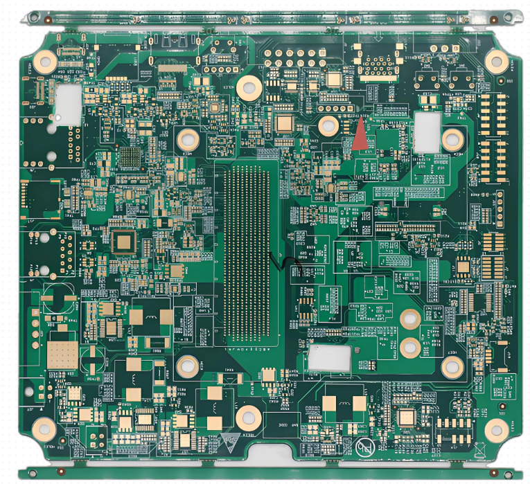
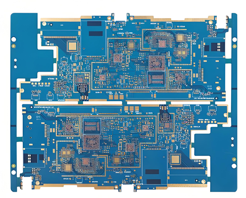
Why Choose Best Technology as Your High Speed PCB Manufacturer?
Selecting the right manufacturing partner is critical for high-speed PCB success. Even a well-designed layout can fail if fabrication tolerances are not tightly controlled.
Best Technology (EBest Circuit) offers a complete high-speed PCB development solution for engineers and OEM companies worldwide.
Key advantages include:
- 1+3 Technical Team Full-Process Service: Each project is supported by one customer engineer and three experienced technical engineers, ensuring rapid technical communication and design optimization.
- Free DFM and BOM Optimization: Senior engineers provide professional DFM review and BOM optimization reports before production begins.
- One-Stop PCB and PCBA Manufacturing: Best Technology integrates PCB fabrication, component sourcing, SMT assembly, and functional testing.
- Rapid Prototype Turnaround: Prototype PCBA projects are typically completed within about 1.5 weeks, allowing engineers to validate designs quickly.
- Certified Manufacturing: The company operates under strict quality systems including ISO9001, ISO13485, IATF16949, and AS9100D.
- Digital Factory and Full Traceability: Advanced MES systems provide component and process traceability in seconds, ensuring manufacturing transparency and reliability.
With over 20 years of PCB and PCBA manufacturing experience, Best Technology supports demanding industries including aerospace, automotive electronics, industrial control, RF communication, and medical equipment.
If you are developing advanced communication hardware, networking equipment, or high-speed computing devices, Best Technology can provide dependable high-speed PCB fabrication and assembly services.
Contact Best Technology today at sales@bestpcbs.com to discuss your next high-speed PCB project.