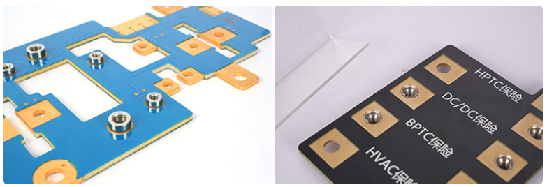
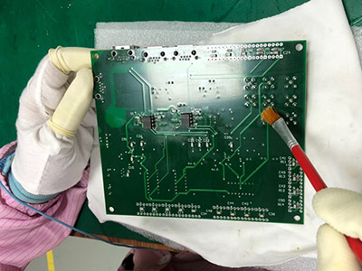
What Is an Extra Thin PCB?
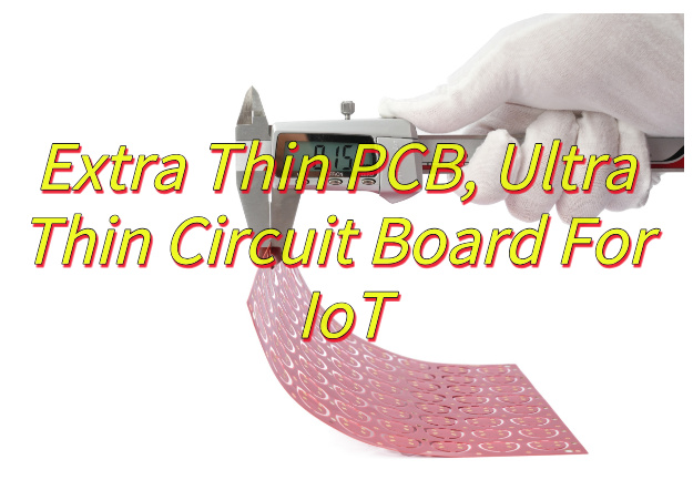
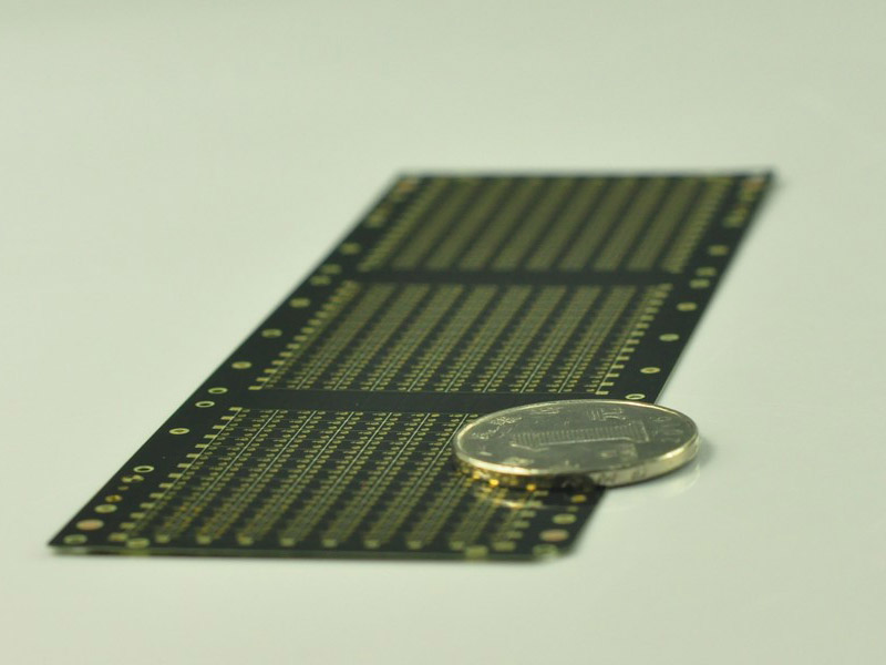
An extra thin PCB is a printed circuit board made with a much thinner profile than standard FR4 boards. In most applications, conventional PCB thickness ranges from 1.0 mm to 2.0 mm. By contrast, extra thin PCBs are typically manufactured in thicknesses such as 0.30 mm, 0.25 mm, 0.20 mm, and even 0.15 mm.
These boards are often called thin PCB, ultra thin PCB, or very thin PCB. They are designed for products where space is limited, weight matters, or a slimmer structure is required for the final assembly.
As electronic devices continue to become smaller, lighter, and more portable, extra thin PCB is being used in a growing number of compact electronic products.
Why Are Extra Thin PCBs Used?
Extra thin PCBs are widely used when a design needs to reduce overall thickness without switching to a flexible circuit. In many cases, they offer a practical middle ground between standard rigid PCBs and FPCs.
Compared with regular FR4 boards, extra thin PCBs help:
- save installation space
- reduce product weight
- support compact internal layouts
- improve product portability
- lower cost compared with some flexible circuit solutions
Extra thin FR4 PCB can also provide a certain degree of bendability during assembly, especially in very low thickness designs. While it is not the same as a flexible PCB, it can still be useful in products that need a slim and semi-rigid structure.
What Thickness Can Extra Thin PCB Reach?
At EBest Circuit, extra thin PCB can be produced in the following common thicknesses:
- 0.15 mm
- 0.20 mm
- 0.25 mm
- 0.30 mm
These boards can be made with or without solder mask, depending on the application requirement. Available copper thickness options include:
- 0.5 oz
- 1 oz
- 2 oz
- 3 oz
The actual structure will depend on the layer count, copper requirement, mechanical strength, and final product usage.
Extra Thin PCB vs Flexible PCB
Extra thin PCB and flexible PCB may look similar in very slim designs, but they are not the same product.
Extra thin PCB is still based on FR4 material, which keeps the board rigid or semi-rigid.
Flexible PCB, on the other hand, is made from flexible substrates such as polyimide and is designed for repeated bending.
Here is the practical difference:
| Item | Extra Thin PCB | Flexible PCB |
|---|---|---|
| Base Material | FR4 | Polyimide / Flex material |
| Structure | Rigid or semi-rigid | Flexible |
| Typical Minimum Thickness | 0.10–0.15 mm | 0.06 mm for 1L FPC |
| Bendability | Limited | Excellent |
| Cost | Usually lower | Usually higher |
| Typical Use | Cards, compact modules, slim devices | Folding, dynamic bending, cable replacement |
If your board thickness needs to go below 0.10 mm, a flexible circuit is usually the better option.
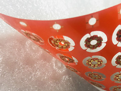
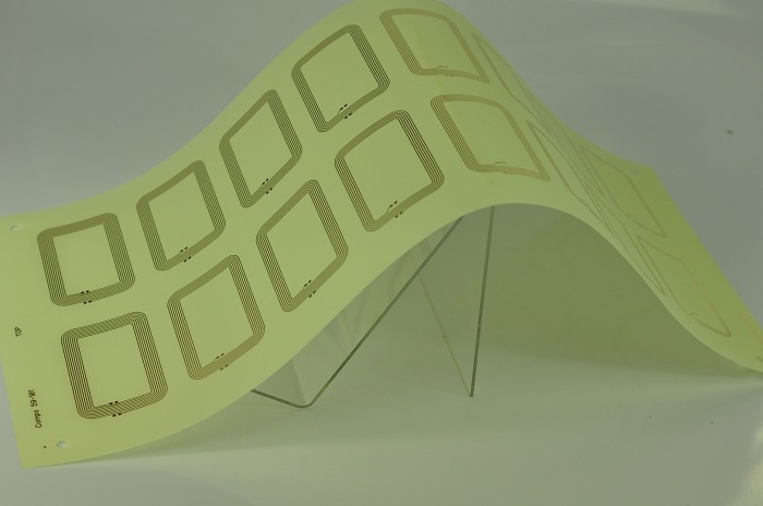
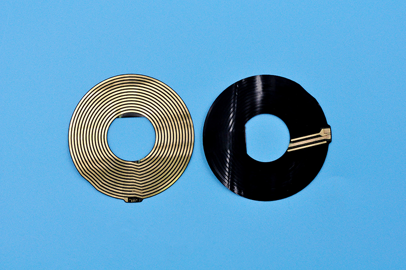
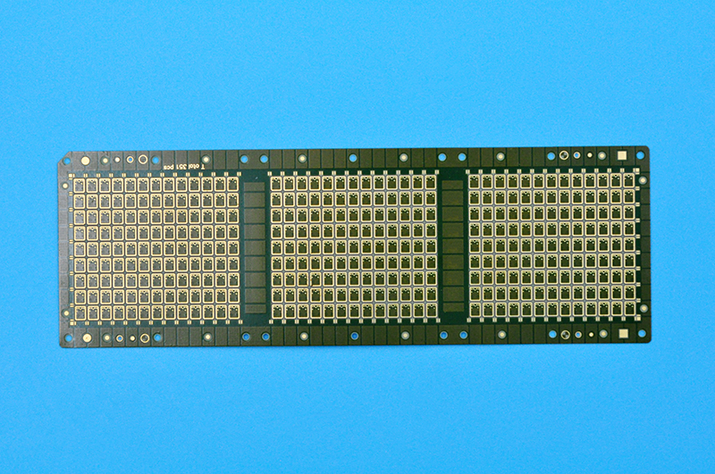
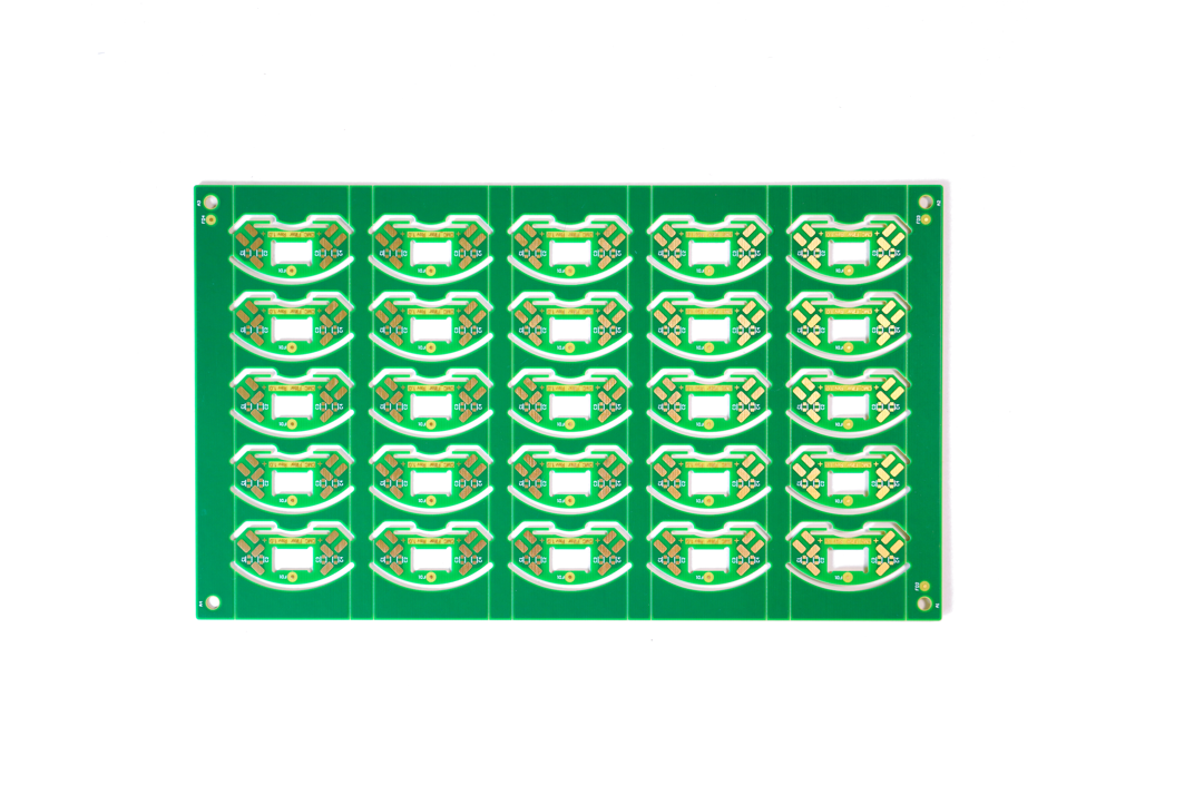
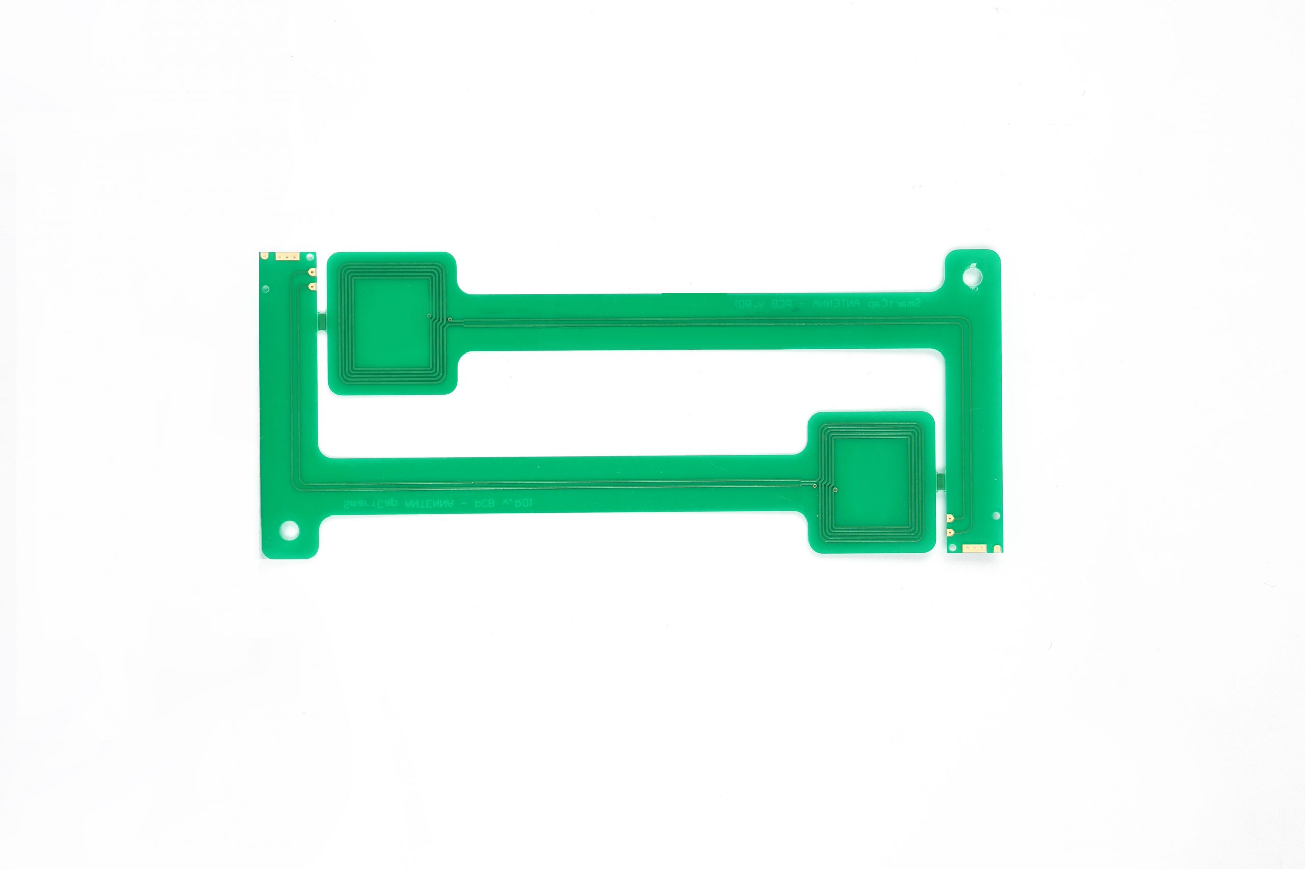
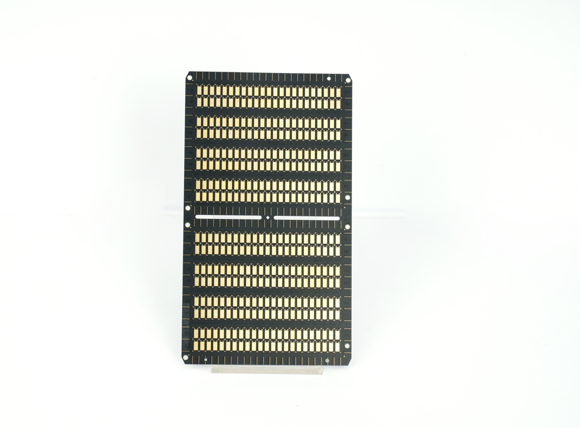
Where Are Extra Thin PCBs Commonly Used?
Extra thin PCBs are commonly used in compact electronic products where traditional PCB thickness is too large for the mechanical design.
Typical applications include:
- SIM cards
- TF cards
- NFC devices
- mobile phone charging modules
- wearable electronics
- sensor cards
- drawing boards
- metro tokens or smart transit devices
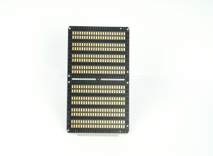
Extra Thin PCB Manufacturing Capability
EBest Circuit provides extra thin PCB manufacturing with stable process control and flexible specification support.
Manufacturing Capability Table
| Item | Capability |
|---|---|
| Base Material | FR4 Tg130 / Tg170 / Tg180 |
| Board Thickness | 0.10 mm – 0.30 mm |
| Copper Thickness | 0.5 oz / 1 oz / 2 oz / 3 oz |
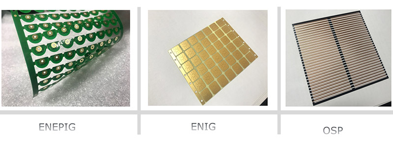
| Surface Finish | ENIG, OSP, ENEPIG, HAL-LF |
| Solder Mask | Bare / White / Black / Blue / Green / Red |
| Silkscreen Color | White / Black |
| Min Via Size | 0.10 mm |
| Min Trace/Space | 4/4 mil |
| Outline Processing | Routing, Punching, V-Cut, Laser Cutting |
| Max Panel Size | 500 × 500 mm or 1000 × 350 mm |
| Min Panel Size | 3.5 × 3.5 mm |
| Min Single Size | 25 × 25 mm |
| Packing | Vacuum Packing |
| Sample Lead Time | 7–9 Days |
| Mass Production Lead Time | 8–10 Days |
What Makes Extra Thin PCB Manufacturing More Challenging?
Although the process flow is similar to standard FR4 PCB manufacturing, extra thin PCB requires much tighter process control.
Because the board is much thinner, it is more sensitive during fabrication. Problems such as panel deformation, handling marks, instability during transfer, and stress during drilling or plating must be controlled carefully.
For this reason, extra thin PCB production often needs:
- more precise panel handling
- better lamination control
- careful drilling and imaging setup
- optimized plating parameters
- suitable support tooling during processing
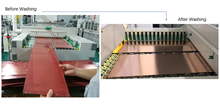
- controlled packing to protect flatness and surface quality
At EBest Circuit, we apply stricter production control for ultra thin boards and use appropriate equipment to ensure smooth processing throughout each manufacturing stage.
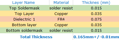
Stack-Up Options for Extra Thin PCB
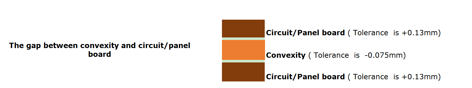
The stack-up of extra thin PCB is usually simpler than standard multilayer boards because the total board thickness is highly restricted.
The board structure is still based on standard FR4 construction, but it uses thinner core and prepreg materials to achieve the required profile.
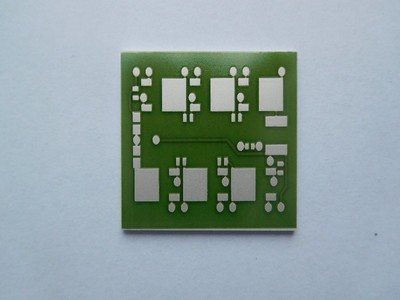
Typical 2-Layer Extra Thin PCB Structure
A 2-layer extra thin PCB usually includes:
- top copper layer
- thin FR4 core
- bottom copper layer
- optional solder mask on one or both sides
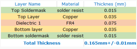
This type of structure is commonly used in card-like products and compact electronic modules.
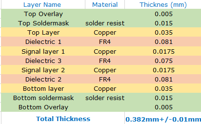
Typical 4-Layer Extra Thin PCB Structure
A 4-layer extra thin PCB is possible, but the thickness is usually around 0.6 mm or above depending on the copper and dielectric design.
A 4-layer thin PCB stack-up generally includes:
- top copper
- thin prepreg/core
- inner copper layers
- thin prepreg/core
- bottom copper
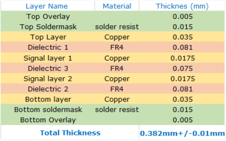
The exact construction should be reviewed based on impedance, mechanical strength, via design, and assembly method.
Why Choose FR4 Extra Thin PCB Instead of Standard PCB?
FR4 extra thin PCB is a strong choice when you need a thinner board but still want the advantages of rigid PCB processing.
It offers several benefits:
- better rigidity than flexible PCB
- lower material cost in many designs
- easier assembly in some rigid product structures
- good compatibility with standard PCB surface finishes
- reliable electrical and mechanical performance for compact devices
For products that do not need repeated bending, an extra thin FR4 PCB can be a cost-effective and stable solution.
How EBest Circuit Supports Extra Thin PCB Projects?
At EBest Circuit, we understand that ultra thin boards require more than just standard PCB production capability. They require careful engineering review, suitable material selection, and stable process control from start to finish.
We support customers with:
- extra thin FR4 material options
- thickness recommendations based on application
- copper and solder mask selection
- stack-up review for 2L and 4L thin boards
- suitable surface finish suggestions
- production control for thin board handling
- vacuum packaging for safe shipment
Whether your project is for wearable electronics, smart cards, NFC modules, or other miniaturized devices, our team can help evaluate the most suitable structure for your design.
FAQ About Extra Thin PCB
1. What is considered an extra thin PCB?
An extra thin PCB usually refers to a rigid FR4 PCB with a thickness significantly below standard boards, typically in the range of 0.10 mm to 0.30 mm.
2. Can extra thin PCB replace flexible PCB?
In some static applications, yes. If the board does not need repeated bending, an extra thin FR4 PCB can be a lower-cost alternative. For dynamic bending, flexible PCB is still the better choice.
3. What is the thinnest FR4 PCB you can make?
Extra thin FR4 PCB can be made as thin as 0.10 mm to 0.15 mm, depending on the layer count and structure.
4. What copper thickness is available for extra thin PCB?
Common copper options include 0.5 oz, 1 oz, 2 oz, and 3 oz.
5. What surface finishes are available?
Available finishes include ENIG, OSP, ENEPIG, and HAL-LF. ENIG and OSP are commonly selected for thin board applications.
6. What applications are suitable for extra thin PCB?
Extra thin PCB is suitable for SIM cards, TF cards, NFC devices, wearable products, charging modules, sensor cards, and other space-limited electronics.
Get a Quote for Extra Thin PCB
If you are looking for a reliable extra thin PCB manufacturer, EBest Circuit can support your project with stable processing capability, thin board experience, and fast response.
From 0.15 mm to 0.30 mm ultra thin FR4 PCB, we help customers turn compact product concepts into manufacturable boards with dependable quality.
Contact us today to discuss your extra thin PCB design and get a quotation for prototype or mass production.