

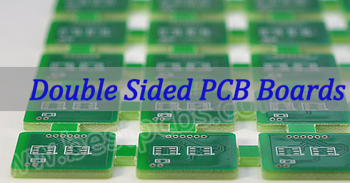
Double sided PCB boards are foundational components that enable complex and compact electronic circuits by providing conductive pathways on both sides of an insulating substrate. This article explores their structure, manufacturing, design, applications, and the critical role they play in building reliable modern electronics.
Balancing performance, reliability, and cost when sourcing double sided printed circuit boards remains a common challenge for engineers and procurement teams.
- Inconsistent board quality paired with high cost or long lead times
- Increased design complexity around vias and component placement
- Risk of defects from poor plating or layer misalignment
- Difficulty matching material performance to application needs
- Slow or expensive prototyping cycles
These challenges underscore the importance of working with a manufacturer that addresses quality, design, and delivery together.
- Strict process control ensures consistent quality from prototype to volume
- Engineering support simplifies layout through DRC and DFM checks
- Precision drilling and plating deliver reliable vias and alignment
- Material options tailored to electrical and thermal requirements
- Fast-turn prototyping enables quick and cost-effective validation
At EBest Circuit (Best Technology), we are a specialized double sided PCB board manufacturer in China committed to excellence. With over two decades of experience, we combine advanced manufacturing capabilities with rigorous quality control to produce reliable, high-performance PCBs. We understand that your electronics are only as good as their foundation, which is why we focus on delivering precision, consistency, and outstanding value for every order, big or small. Pls feel free to contact us at sales@bestpcbs.com to discuss your PCB or PCBA project needs. Our capabilities span FR4 PCB fabrication, flexible and rigid-flex circuitry, metal core and ceramic PCBs, supported by PCB layout and box-build integration.
What Are Double Sided PCB Boards?
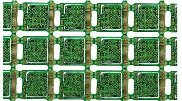
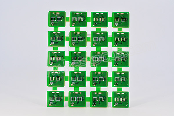
A Double Sided PCB (Printed Circuit Board) is a circuit board that has conductive copper layers on both the top and bottom sides of an insulating substrate. The two layers are electrically connected using plated-through holes (PTHs), commonly known as vias. This simple yet powerful architecture allows circuits to cross over each other by moving from one side to the other, enabling more complex and dense circuitry than what is possible with a single sided PCB board.
- Core Structure: An insulating core (like FR4) clad with copper foil on both sides.
- Key Feature: Use of vias (holes plated with conductive material) to create electrical connections between the top and bottom layers.
- Primary Benefit: Doubles the available area for routing traces compared to single-sided boards, allowing for more sophisticated circuits in a similar footprint.
In summary, double sided PCB boards serve as a critical stepping stone between simple single-layer boards and complex multi-layer boards, offering an optimal balance of functionality, cost, and manufacturing complexity for a vast array of electronic devices.
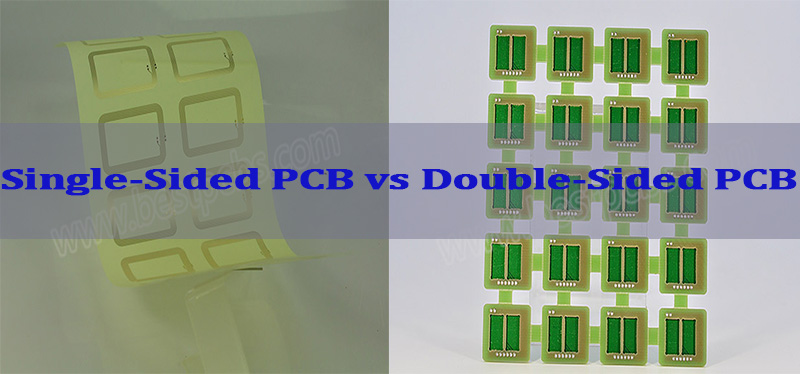
What Is the Difference Between Single and Double Sided PCB?
The fundamental difference between a single sided PCB and a double sided PCB lies in copper layer availability and routing flexibility. This distinction directly impacts circuit density, design freedom, manufacturing complexity, and overall cost, making it a key decision point during early PCB design.
Single vs Double Sided PCB Comparison
| Feature | Single-Sided PCB | Double-Sided PCB |
|---|---|---|
| Copper Layers | 1 | 2 |
| Circuit Density | Low | Medium |
| Routing Capability | Limited | More flexible |
| Via Usage | Not required | Required |
| Design Complexity | Simple | Moderate |
| Cost Level | Low | Medium |
| Typical Applications | Basic circuits | Moderate-complex circuits |
| Manufacturing Steps | Basic etching | Drilling + through-hole plating |
Practical Design Interpretation
A single sided PCB places all copper traces on one surface, which inherently limits routing options. Once traces begin to intersect or component density increases, designers quickly encounter layout constraints. This is why single sided designs are typically used in low-complexity products such as simple power supplies, LED boards, and basic consumer electronics.
In contrast, double sided PCB boards utilize copper on both the top and bottom layers. Electrical connections between the two sides are achieved through plated through-holes, allowing traces to cross layers without interference. This added routing freedom enables higher component density and more compact layouts without the cost escalation associated with multilayer PCBs.
From a cost–performance standpoint, double sided PCBs represent a balanced solution. They are more expensive than single sided boards due to additional drilling and plating steps, but they remain significantly more economical than multilayer constructions. As a result, they are widely adopted in consumer electronics, automotive control modules, industrial equipment, and communication devices.
In practice, when circuit requirements exceed the routing capacity of a single copper layer, double sided PCB boards become the logical next step. They provide improved electrical routing, better space utilization, and broader application flexibility while maintaining manageable manufacturing costs.
How Are Double Sided Copper Clad Board Structured?
A double sided copper clad board is the raw material from which finished PCBs are made. Its structure is the foundation of the board’s performance.
The basic structure consists of three key layers:
- Top Copper Layer: A thin foil of conductive copper, typically 0.5 oz to 2 oz in weight, that will be etched to form the circuit pattern.
- Dielectric Substrate Core: The insulating layer that provides mechanical support and electrical isolation. FR4 glass epoxy is the most common material.
- Bottom Copper Layer: A second copper foil layer identical to the top, allowing for circuitry on both sides.
For the finished PCB, additional elements are added:
- Solder Mask: A protective polymer layer (usually green) applied over the copper traces, leaving only the pads and vias exposed.
- Silkscreen: The white lettering used for component labels, logos, and test points.
- Surface Finish: A coating (like HASL, ENIG, or OSP) applied to exposed copper to prevent oxidation and enhance solderability.
- Plated-Through Holes (PTHs): The metallized holes that connect the top and bottom copper layers, forming the essential 3D interconnect pathway.
This layered structure of a double-sided copper clad laminate PCB circuit board is precisely engineered to provide reliable electrical performance and mechanical stability.
How Is the Double-Sided PCB Manufacturing Process?
The double-sided PCB manufacturing process involves a series of precise steps to transform a raw double sided copper clad laminate into a functional circuit board.
Core Process Steps:
- Drilling: Precise CNC machines drill holes for component leads and, critically, for vias that will connect both layers.
- Through-Hole Plating: This is the defining step for double-sided boards. The drilled holes are chemically coated with a thin layer of copper, creating an electrical conduit between the top and bottom layers.
- Imaging & Pattern Transfer: A photoresist is applied, and the circuit design is transferred using UV light through a photomask. The exposed (or unexposed, depending on the process) resist is then developed away.
- Etching: The board is immersed in a chemical etchant (e.g., ferric chloride) which removes the unwanted copper, leaving only the desired circuit traces protected by the resist.
- Stripping & Cleaning: The remaining photoresist is stripped off, revealing the copper circuitry.
- Solder Mask Application: The solder mask ink is applied, exposed, and developed to open windows over pads and vias.
- Surface Finishing: A final coating (e.g., ENIG, HASL) is applied to the exposed copper to ensure solderability and protect against corrosion.
- Silkscreen & Electrical Test: Component labels are printed, and each board undergoes electrical testing to verify connectivity and the absence of short circuits.
In closing, this multi-stage process, especially the through-hole plating, is what enables the functionality of double sided PCB boards, ensuring reliable vertical interconnects that are crucial for their operation.
What Materials Are Commonly Used in Double Sided Printed Circuit Boards PCB?
The choice of material directly impacts the performance, reliability, and cost of the final board. The most common material is FR4, but alternatives exist for specific needs.
Standard Material:
- FR4 (Flame Retardant 4): A composite of woven fiberglass cloth and an epoxy resin binder. It is the industry workhorse due to its excellent mechanical strength, good electrical insulation, moisture resistance, and relatively low double sided PCB board price.
Specialized Materials:
- High-Tg FR4: For applications requiring higher thermal stability (e.g., lead-free soldering).
- Polyimide: Used for double sided flexible PCB board applications where the board must bend or flex.
- Rogers or Taconic Laminates: High-frequency materials with stable dielectric constants for RF/microwave applications.
- Metal-Clad (e.g., Aluminum): Used for boards requiring excellent thermal dissipation (LED lighting, power converters).
- 94V0 Rated FR4: A specific flammability rating (double-sided 94V0 PCB board) required for certain safety-critical applications.
To sum up, selecting the right base material—whether standard FR4 double-sided PCB board or a specialized alternative—is a critical first step in designing a reliable double sided copper PCB circuit board for any application.
What Design Rules Apply to Double Sided Printed Circuit Boards PCB Boards?
Effective double sided PCB design requires adhering to a set of rules to ensure manufacturability, reliability, and performance. These rules are often defined as Design for Manufacturability (DFM) guidelines.
Key Design Rules to Follow:
- Trace Width/Spacing: Determine based on current carrying capacity and voltage. General rules (e.g., 6/6 mil for signal traces) must be confirmed with your manufacturer’s capabilities.
- Via Specifications: Define hole size (drill diameter) and pad size (annular ring). Ensure the annular ring is sufficient to guarantee a reliable connection after drilling tolerances.
- Component Placement: Place components logically, typically on the top side. Consider soldering process (wave soldering may require specific bottom-side component orientation).
- Layer Coordination: Use one layer primarily for horizontal traces and the other for vertical traces to simplify routing. Assign one layer as a ground plane if possible for better noise immunity.
- Thermal Management: Provide adequate thermal relief for pads connected to large copper pours (planes) to prevent solder issues during assembly.
- Solder Mask & Silkscreen: Clearly define solder mask expansion and ensure silkscreen text does not cover pads.
To wrap up, by following these double sided PCB design rules and consulting your manufacturer’s DFM guidelines early, you can avoid costly delays and ensure your custom double sided PCB board is produced correctly the first time.
How Do Copper PCB Board Double Sided Perform Electrically and Thermally?
The performance of a double sided copper PCB board is intrinsically linked to its material properties and construction.
Electrical Performance:
- Conductivity: The copper traces provide low-resistance pathways for electrical signals and power. Thicker copper (e.g., 2 oz) lowers resistance for high-current paths.
- Signal Integrity: The proximity of traces on two layers can lead to crosstalk. Proper spacing, use of ground pours, and careful routing are essential. The dielectric constant (Dk) of the substrate material affects signal speed.
- Impedance Control: For high-speed signals, the trace geometry (width, thickness) and distance to the reference plane (in more complex stack-ups) must be controlled to achieve a target impedance.
Thermal Performance:
- Heat Dissipation: Copper is an excellent thermal conductor. Double sided copper PCB boards can dissipate heat more effectively than single-sided boards by using large copper areas (pours) on both layers.
- Thermal Vias: Arrays of vias filled or plugged with thermal paste can be used to transfer heat from a component on the top layer to a large copper area on the bottom layer, significantly improving cooling.
- Material CTE: The Coefficient of Thermal Expansion (CTE) of the substrate should be matched to components (like BGAs) to prevent solder joint stress during temperature cycling.
In brief, the structural advantages of a double sided copper clad PCB board—namely, the dual conductive layers and through-hole vias—provide designers with powerful tools to manage both electrical signal quality and thermal energy, which are crucial for reliable electronics.
What Are the Advantages of a Double Layer PCB?
Choosing a double sided PCB board over a single-sided one offers several compelling benefits that justify its slightly higher cost for many applications.
Core Advantages:
- Increased Circuit Density: The primary advantage. Two layers allow traces to cross by switching sides via vias, accommodating more components and complex circuitry in a smaller area.
- Enhanced Design Flexibility: Designers are not constrained by the routing limitations of a single layer, allowing for more optimized and efficient layouts.
- Improved Signal and Power Integrity: The bottom layer can be used as a dedicated ground plane or power plane, reducing electromagnetic interference (EMI), crosstalk, and providing a stable reference for signals.
- Better Thermal Management: The additional copper layer acts as a heat spreader. Thermal vias can be used to conduct heat away from hot components to the opposite side or to an external heatsink.
- Reduced Overall Size and Weight: By enabling higher density, the physical footprint of the electronic assembly can often be reduced.
- Cost-Effective Complexity: For circuits too complex for a single layer but not demanding enough for a multilayer PCB, double-sided boards offer the perfect balance of capability and double sided PCB boards cost.
In summary, these advantages make double sided printed circuit boards (PCB) the most popular and versatile board type, widely used across consumer, industrial, and automotive electronics.
How to Use Double Sided PCB Board
Using a finished double sided PCB board involves the standard electronics assembly process. Knowing how to use double sided PCB prototyping board is specifically crucial for developers.
For Finished/Production Boards:
- Component Procurement: Gather all components (resistors, ICs, connectors) per the Bill of Materials (BOM).
- Soldering: Apply solder paste to pads (for SMDs), place components, and use a reflow oven or hot plate. For through-hole components, insert leads and solder manually or via wave soldering.
- Inspection & Testing: Visually inspect for solder bridges or tombstoning. Perform in-circuit testing (ICT) or functional testing.
How to Use Double Sided PCB Prototyping Board:
Prototyping boards, or perfboards, are pre-drilled boards with copper pads or strips. Here’s how to use them:
- Planning: Map your circuit diagram onto the physical board. Use the top and bottom sides strategically for different parts of the circuit.
- Component Placement: Insert component leads through the holes from the top side.
- Interconnection: On the bottom side, use insulated wires or the existing copper patterns to make connections. The key step for double-sided boards is creating connections between the two sides.
- Creating Vias: To connect a trace from the top to the bottom, use a small piece of solid wire (a “via wire”). Solder one end to the pad/trace on the top, pass the wire through a nearby hole, and solder it to the corresponding pad/trace on the bottom.
- Testing: Continuously test sections of your circuit as you build to isolate faults.
To summarize, whether using a custom fabricated board or a universal double sided prototype PCB universal printed circuit board, the principle remains: leverage both sides for routing and use reliable methods (manufactured PTHs or manual via wires) to interconnect them.
Where Are Double Sided Copper Clad Laminate PCB Circuit Board Commonly Used?
The versatility of double sided copper clad laminate PCB circuit boards makes them ubiquitous in modern electronics. Their double-sided PCB applications span nearly every industry.
Common Application Areas:
- Consumer Electronics: Power supplies, audio amplifiers, gaming peripherals, and smart home devices.
- Automotive Electronics: Engine control units (ECUs), LED lighting modules, infotainment systems, and sensor interfaces.
- Industrial Controls: PLCs, motor drives, power converters, and instrumentation panels.
- Telecommunications: Routers, modems, network switches, and RF modules (often using specialized high-frequency laminates).
- Medical Devices: Patient monitors, diagnostic equipment, and portable medical tools.
- Prototyping & R&D: The double sided PCB prototyping board is a staple in engineering labs for developing and testing new circuit ideas.
To draw this to a close, from the cheap double sided PCB board in a toy to the robust board in an automotive module, double-sided technology is the backbone of a massive range of electronic products due to its optimal cost-to-performance ratio.
What Quality Factors Determine the Reliability of Double Sided Copper PCB Circuit Board?
The reliability of a double sided copper PCB circuit board is not accidental; it is engineered through strict control of several quality factors.
Critical Quality Factors:
- Copper Plating Quality: The integrity of the plated-through holes (PTHs) is paramount. Voids, cracks, or insufficient plating thickness in the barrel of the hole can lead to intermittent or open connections.
- Layer-to-Layer Registration: Precise alignment between the top and bottom layers and the drilled holes is essential. Misregistration can cause broken annular rings or shorts.
- Material Integrity: The substrate must be free of voids/delamination and have the specified Tg, dielectric constant, and flame retardancy (e.g., 94V0).
- Solder Mask Adhesion: The solder mask must properly adhere to the copper and substrate, with precise opening over pads. Poor adhesion can lead to mask peeling and solder bridging.
- Surface Finish Durability: The finish (ENIG, HASL, etc.) must protect the copper from oxidation and provide a reliable, solderable surface throughout the product’s shelf life and assembly process.
- Electrical Test Coverage: 100% electrical testing (flying probe or fixture-based) is crucial to verify continuity (no opens) and isolation (no shorts) across the entire board.
As a final remark, a reliable high-quality double sided PCB board is the result of meticulous attention to these factors throughout the double-sided PCB manufacturing process, ensuring the final product performs consistently in its end application.
To encapsulate the discussion, double sided PCB boards are the essential bridge between simple and highly complex circuits, providing the critical foundation for countless modern electronic devices. This article has explored their design, manufacturing, materials, and the key factors that define their quality and reliability.
For your next project that demands robust, compact, and cost-effective circuitry, a well-designed double sided printed circuit board (PCB) is likely the optimal solution. Partnering with an experienced manufacturer is key to unlocking this potential.
EBest Circuit (Best Technology) specializes in delivering high-quality, reliable double sided PCB boards. As a trusted China double sided PCB board manufacturer, we provide comprehensive support from double sided PCB board prototype to full-scale production, ensuring your electronics are built on a foundation of quality. Pls feel free to contact us anytime for a quote or technical consultation via sales@bestpcbs.com
FAQs
Q: What Is the Double Sided Copper Clad PCB Board?
A: It refers to the raw, un-etched base material—an insulating substrate (like FR4) with a layer of copper foil laminated to both of its sides. It is the starting point for manufacturing a finished double sided PCB board.
Q: What Are the Two Sides of a PCB Called?
A: They are conventionally called the Top Layer (or Component Side) and the Bottom Layer (or Solder Side). The Top Layer is usually where most components are placed.
Q: What Is a Single Sided PCB Used For?
A: A single sided PCB is used for very simple, low-cost electronic circuits where component count and routing are minimal, such as in basic power supplies, calculators, toys, and LED light boards.
Q: Are Motherboards Just PCBs?
A: Motherboards are a highly complex type of PCB. They are typically multilayer circuit boards (often 6-12 layers or more), integrating double sided PCB technology within a much denser stack-up to accommodate CPUs, RAM, and high-speed buses.
Q: What Is V in PCB Board?
A: “V” often refers to Voltage. In specific contexts like “94V0,” it is a flammability rating (UL94-V0) indicating the material’s ability to self-extinguish, a critical safety standard for PCBs.
Q: What Is a Trace on a PCB?
A: A trace is the conductive pathway, typically made of copper, etched onto the PCB substrate. It functions as the “wire” that carries electrical signals and power between components.
Q: How Do I Make a Double Sided PCB Board?
A: While hobbyists can make simple boards using toner transfer and chemical etching, producing reliable double sided PCB boards with plated-through holes requires professional equipment. The professional process involves:
1) Drilling holes,
2) Electroless copper deposition to make holes conductive,
3) Electroplating to build up copper,
4) Photoresist imaging,
5) Etching,
and 6) Applying solder mask and finish.
For reliable results, it is recommended to use a professional double sided PCB board factory in China like EBest Circuit.