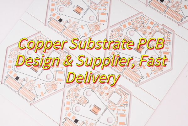
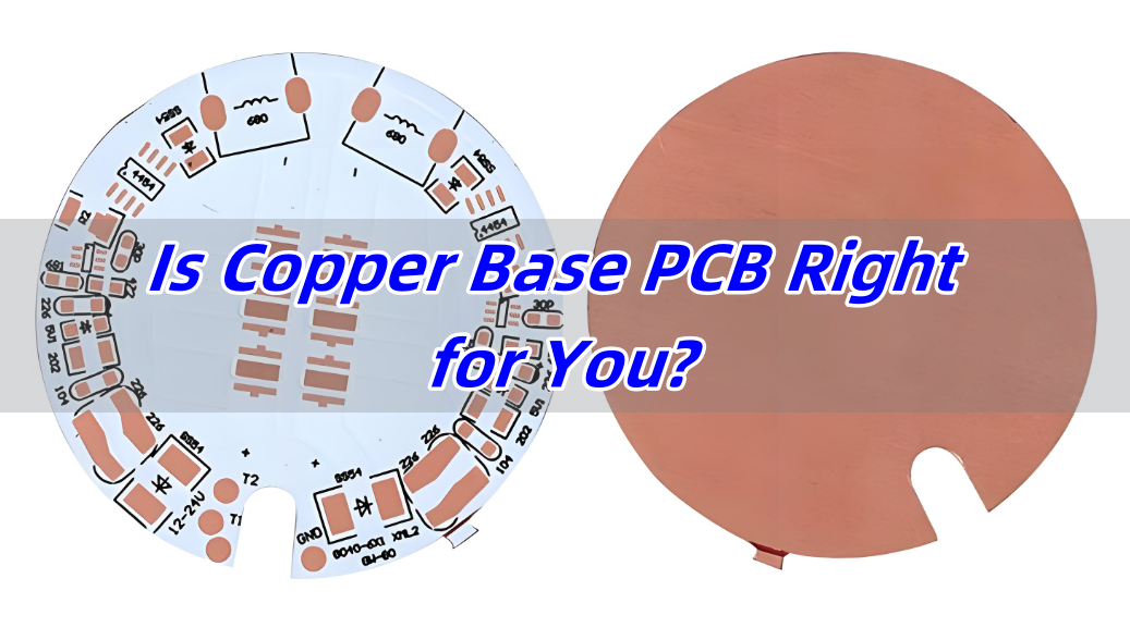
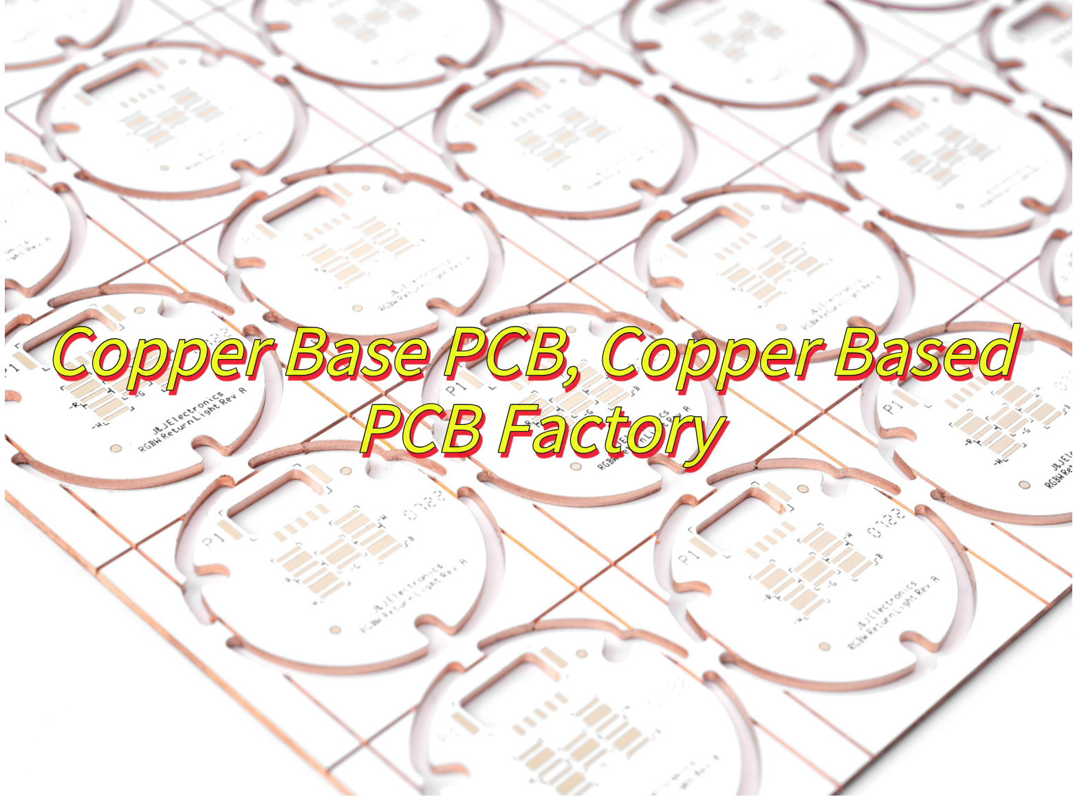
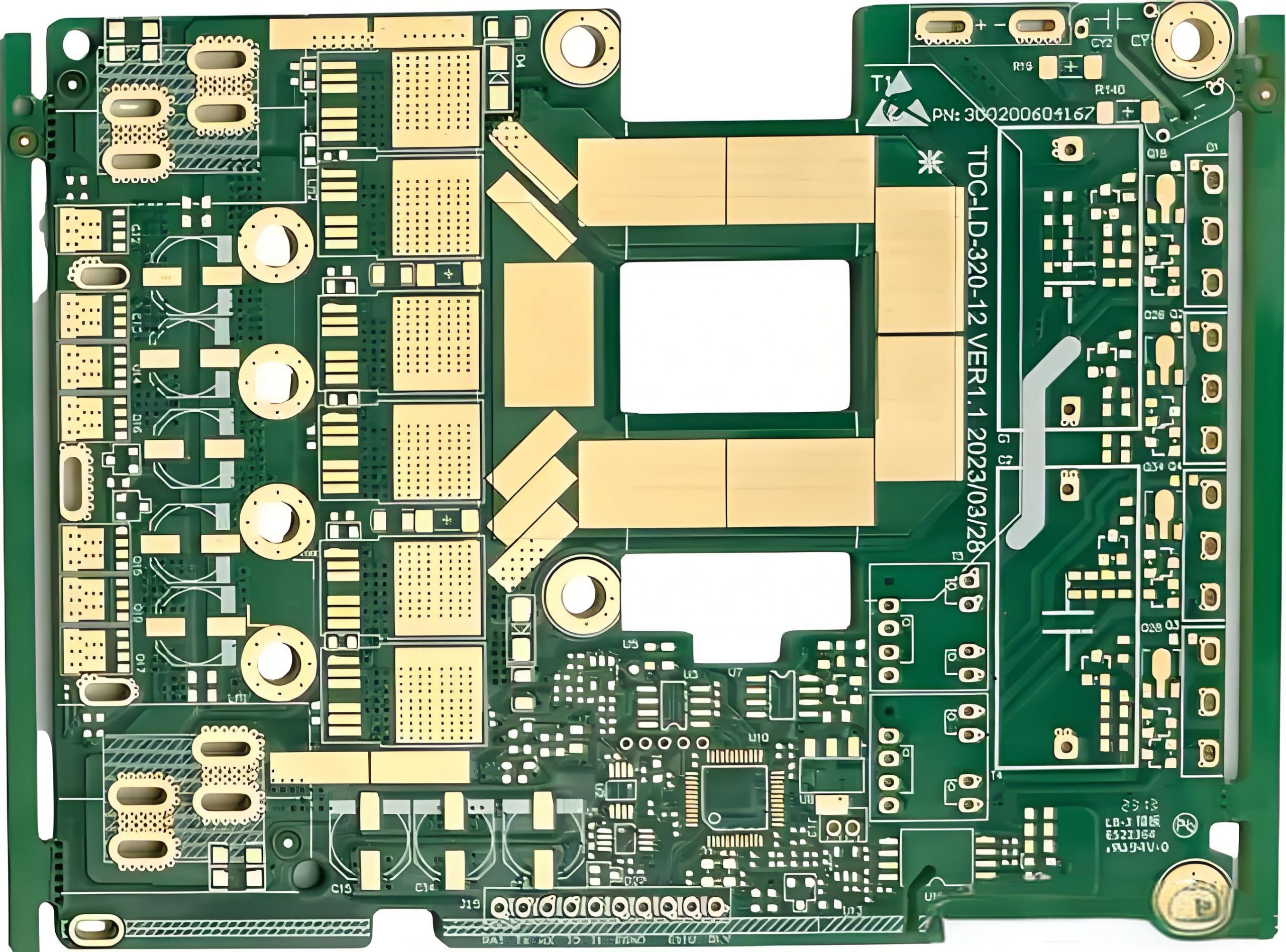
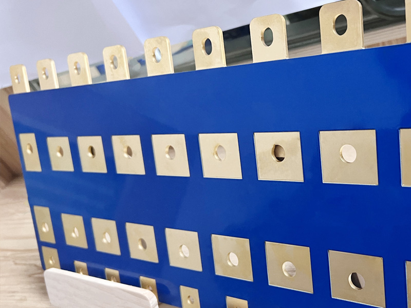
Choose EBest As Your First Copper Base PCB Manufacturer
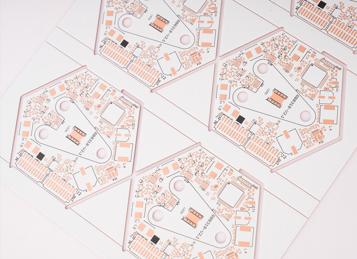
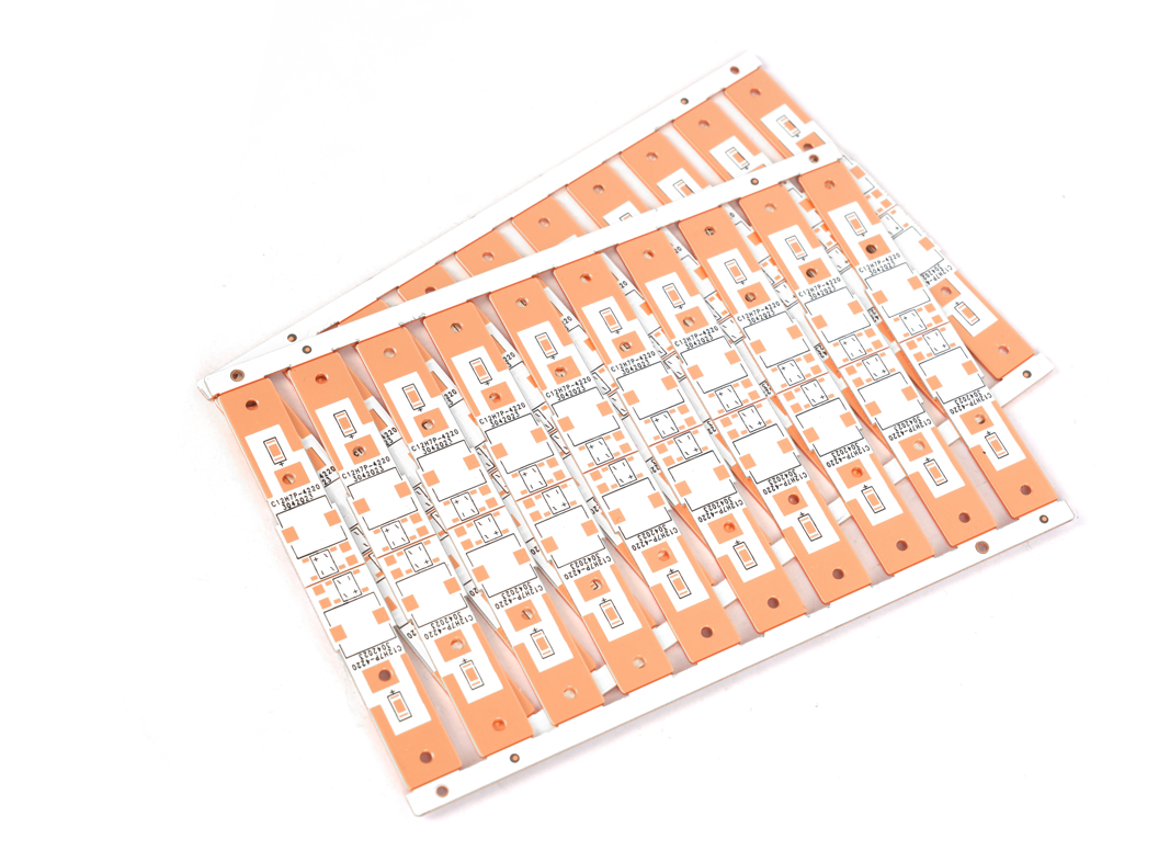
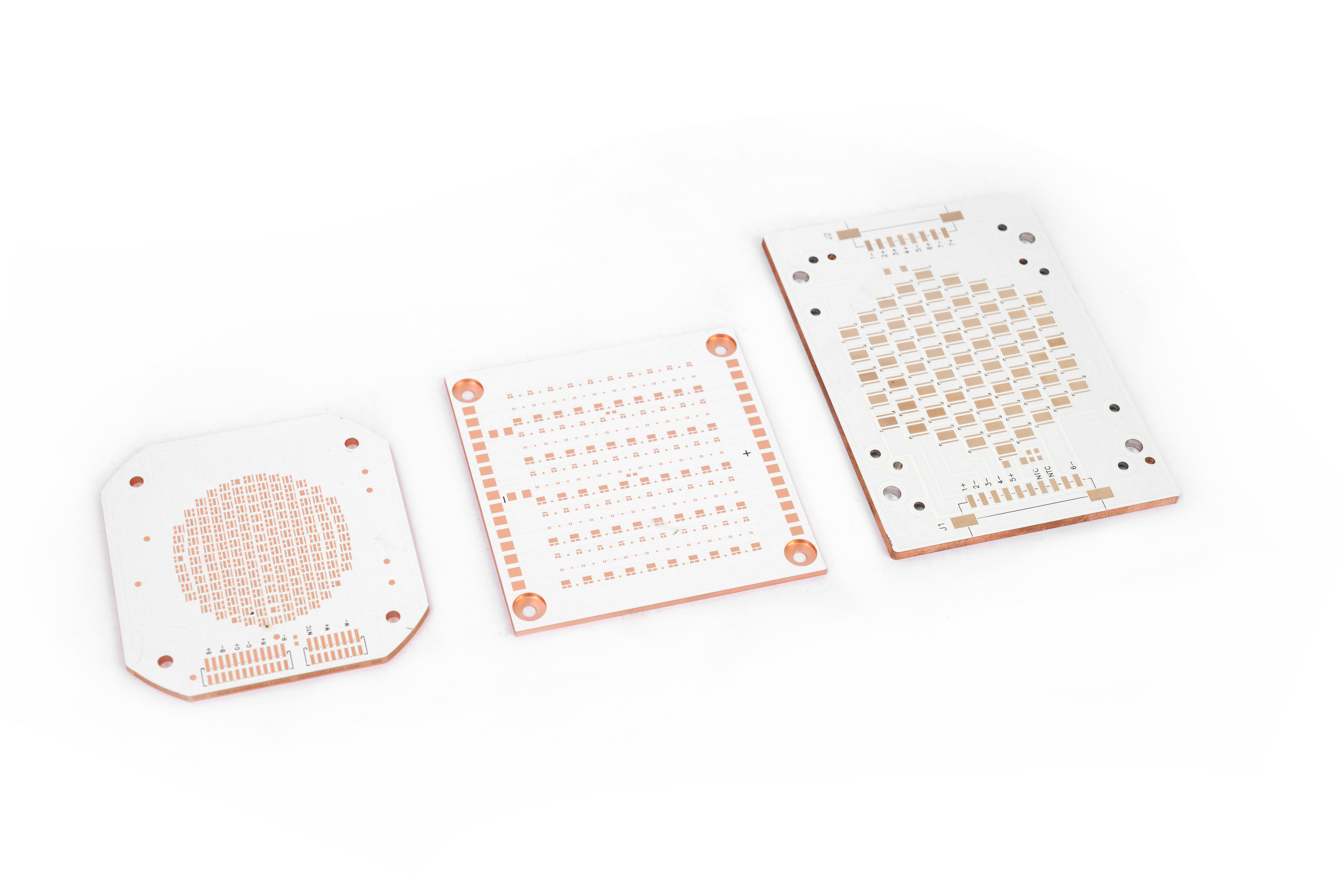
When searching for a reliable Copper Base PCB manufacturer, EBest stands out as the top choice for global electronics businesses and engineers. Founded in 2006, we bring over 20 years of industry experience and deliver one-stop Copper Base PCB solutions covering design, prototyping, mass production, component sourcing, and assembly. Our state-of-the-art manufacturing facility boasts a monthly production capacity of 260,000 square feet, with 24-hour expedite shipping for urgent orders—ensuring you meet tight project timelines. Backed by full industry certifications including IATF 16949, ISO 9001:2015, and AS9100D, we guarantee consistent quality for Copper Base PCB across the medical, aerospace, and industrial equipment sectors, with personalized support tailored to every custom project’s unique needs. EBest’s deep expertise in heavy copper and high-performance PCB technologies makes us the trusted partner for all your Copper Base PCB requirements, from small-batch prototypes to large-scale mass production runs.
What Do Engineers Care About In Copper Base PCB Design? Solve Pain Points With EBest
Key Design Challenges Engineers Face For Copper Base PCB
Engineers designing Copper Base PCB consistently grapple with three core pain points: optimizing thermal conductivity for high-power applications, achieving precise impedance control to avoid signal interference, and ensuring structural compatibility with rigid or flexible PCB integration. Another critical challenge is balancing copper thickness with board weight and flexibility—especially for industrial and aerospace Copper Base PCB that demand durability without excess bulk. Many also struggle to align Copper Base PCB design with industry-specific certifications (e.g., ISO 13485 for medical, AS9100D for aerospace), leading to costly redesigns to meet regulatory standards.
EBest’s Copper Base PCB Design Solutions For Every Challenge
EBest’s engineering team solves these design pain points with tailored, industry-specific strategies. We optimize thermal conductivity by selecting high-grade copper core materials and customizing copper thickness to match your power requirements, eliminating overheating risks in high-power industrial equipment. Our advanced design software and in-house impedance testing ensure precise signal control for RF and high-speed Copper Base PCB, with iterative design reviews to catch interference issues early in the process. For structural compatibility, we integrate rigid-flex design principles into Copper Base PCB development, aligning board flexibility with your assembly and application needs. Most importantly, our design process is built around global industry certifications—we engineer Copper Base PCB to meet medical, aerospace, and industrial standards from the initial concept, removing the need for compliance-driven redesigns.
Partner With EBest For Your Copper Base PCB Design Needs
Whether you’re designing a Copper Base PCB for medical imaging devices, aerospace avionics, or heavy-duty industrial machinery, EBest’s design team combines technical precision with application-focused expertise to deliver designs aligned with your performance, compliance, and production goals. Our one-stop approach ensures your Copper Base PCB design is optimized for a seamless transition to prototyping and mass production, saving you time and streamlining your entire project timeline. Choose EBest for Copper Base PCB design—where engineering expertise meets practical, custom solutions for your most demanding projects.
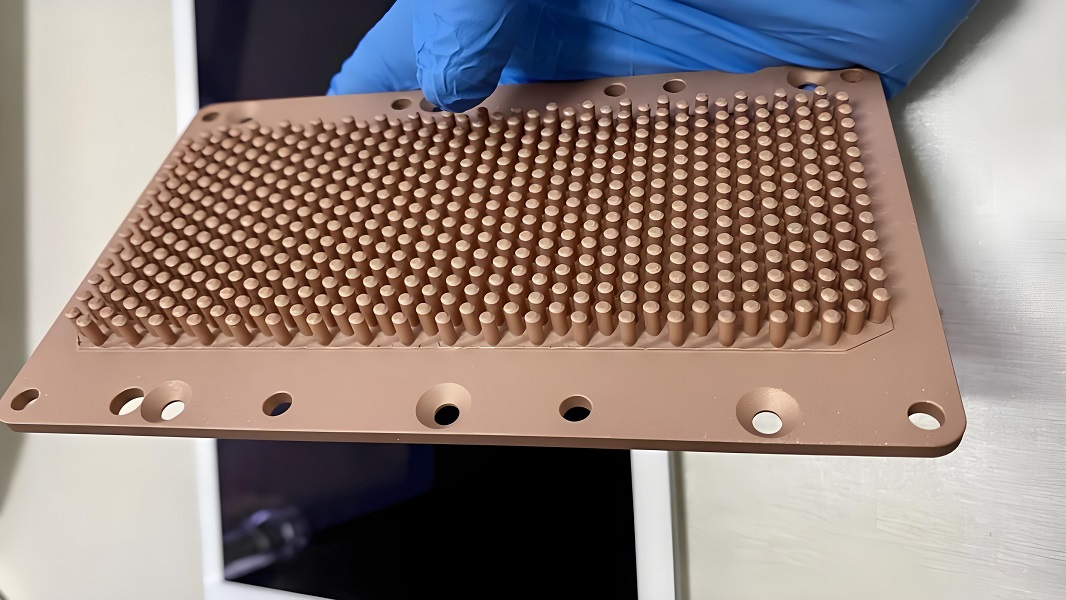
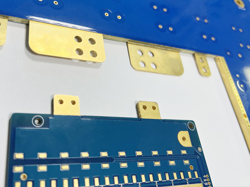
Copper Base PCB Prototype: Overcome Prototyping Pain Points With EBest
Top Prototyping Pain Points For Copper Base PCB
Engineers and product developers face distinct hurdles when creating Copper Base PCB prototypes: lengthy lead times that delay product testing, inconsistent prototype quality that fails to reflect mass production performance, and limited customization options for small-batch runs. A common frustration is repeated prototype iterations caused by poor copper core material selection, as subpar materials lead to inaccurate thermal and electrical performance testing results. Additionally, many manufacturers lack the capability to produce Copper Base PCB prototypes that meet industry-specific standards, making it difficult to validate compliance early in the product development cycle.
EBest’s Copper Base PCB Prototype Solutions To Accelerate Your Project
EBest addresses every Copper Base PCB prototyping pain point with speed, quality, and full customization at the core. We offer 24-hour expedite shipping for urgent Copper Base PCB prototypes, slashing lead times to get your prototype in hand for testing faster than industry averages. Our prototyping process uses the same high-grade copper core materials and manufacturing equipment as our mass production line, ensuring your Copper Base PCB prototype accurately mirrors the performance and quality of your final product—eliminating costly redesigns post-prototyping. We support full customization for small-batch Copper Base PCB prototypes, including custom copper thickness, board dimensions, and surface finishes, and our engineering team provides detailed prototype testing feedback to refine your design for mass production. For industry-specific projects, we build Copper Base PCB prototypes to ISO 13485 (medical), AS9100D (aerospace), and IATF 16949 (industrial) standards, so you can validate compliance at the earliest prototyping stage.
Choose EBest For Your Copper Base PCB Prototype Development
EBest’s Copper Base PCB prototyping service is engineered for engineers who need fast, reliable, and industry-compliant prototypes to advance product development. Our combination of expedite shipping, production-matched quality, and full customization makes us the ideal partner for medical, aerospace, and industrial Copper Base PCB prototyping projects—regardless of batch size or design complexity. Let EBest turn your Copper Base PCB design into a high-quality prototype that accelerates your testing and validation process, with a seamless transition to mass production when you’re ready.
Copper Base PCB Assembly: Resolve Assembly Challenges With EBest’s Expertise
Critical Assembly Pain Points For Copper Base PCB
Copper Base PCB assembly comes with unique challenges that can derail production timelines and reduce product reliability: poor thermal management during soldering that damages copper core materials, component misalignment on thick copper PCBs, and difficulty sourcing compatible components for high-power Copper Base PCB applications. Engineers also struggle with assembly processes that fail to meet the strict quality standards of the medical and aerospace industries, leading to high defect rates and costly rework. Another common issue is limited assembly flexibility for custom Copper Base PCB designs, as many manufacturers use one-size-fits-all assembly processes that do not account for the unique properties of copper core PCBs.
EBest’s Copper Base PCB Assembly Solutions For Flawless Production
EBest’s Copper Base PCB assembly service leverages specialized equipment and industry expertise to solve these challenges for medical, aerospace, and industrial projects. We use temperature-controlled soldering processes for Copper Base PCB assembly, preventing thermal damage to copper core materials and ensuring strong, reliable solder joints—critical for high-power applications. Our automated assembly line features high-precision component placement technology, eliminating misalignment issues even on thick, heavy copper Copper Base PCB. As a one-stop provider, we offer full component sourcing for Copper Base PCB assembly, matching high-quality, industry-compliant components to your design’s power and performance requirements—saving you time and guaranteeing component compatibility. Our assembly process is certified to ISO 13485, AS9100D, and IATF 16949, so your Copper Base PCB assembly meets the strict quality and compliance standards of the medical, aerospace, and industrial equipment industries, with zero-defect production as our core goal. We also provide flexible assembly processes for custom Copper Base PCB designs, tailoring our approach to your board’s unique properties and assembly requirements.
Trust EBest For Your Copper Base PCB Assembly Needs
Whether you need small-batch or large-scale Copper Base PCB assembly for medical devices, aerospace systems, or industrial machinery, EBest’s one-stop assembly service delivers uncompromising quality, full compliance, and on-time delivery. Our integration of component sourcing, precision assembly, and industry certification ensures your Copper Base PCB assembly process is seamless from start to finish, with no gaps in quality or regulatory compliance. Choose EBest for Copper Base PCB assembly—where specialized copper core expertise meets reliable, scalable production for all your PCB projects.
Why Choose EBest For Your Copper Base PCB Projects?
EBest is the premier choice for Copper Base PCB design, prototyping, and assembly for three core reasons: 20+ years of specialized copper core expertise, end-to-end one-stop solutions, and industry-leading quality and compliance. Our team of PCB engineers has deep experience in Copper Base PCB technologies for the medical, aerospace, and industrial equipment sectors, with a proven track record of delivering custom solutions that meet the most demanding performance requirements. As a one-stop provider, we handle every step of your Copper Base PCB project—from initial design and prototyping to mass production, component sourcing, and assembly—eliminating the need to work with multiple vendors and streamlining your project timeline. Our manufacturing facility is certified to IATF 16949, ISO 9001:2015, ISO 13485:2016, AS9100D, REACH, RoHS, and UL, so every Copper Base PCB we produce meets global industry standards for quality, safety, and compliance. We also offer unrivaled speed, with 24-hour expedite shipping for urgent Copper Base PCB orders and a monthly production capacity of 260,000 square feet (28,900 square meters) to support both small-batch prototypes and large-scale mass production. EBest prioritizes customer satisfaction, with personalized support for every Copper Base PCB project—our team works closely with you to understand your unique needs and deliver tailored solutions aligned with your product goals. Finally, our ongoing commitment to research and development ensures we stay ahead of industry trends in Copper Base PCB technology, continuously innovating our design, prototyping, and assembly processes to deliver the most advanced copper core PCB solutions for your business.
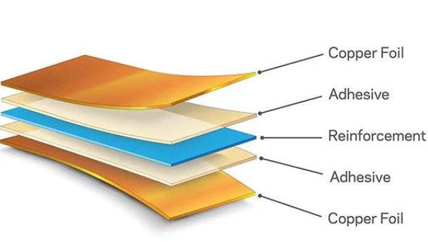
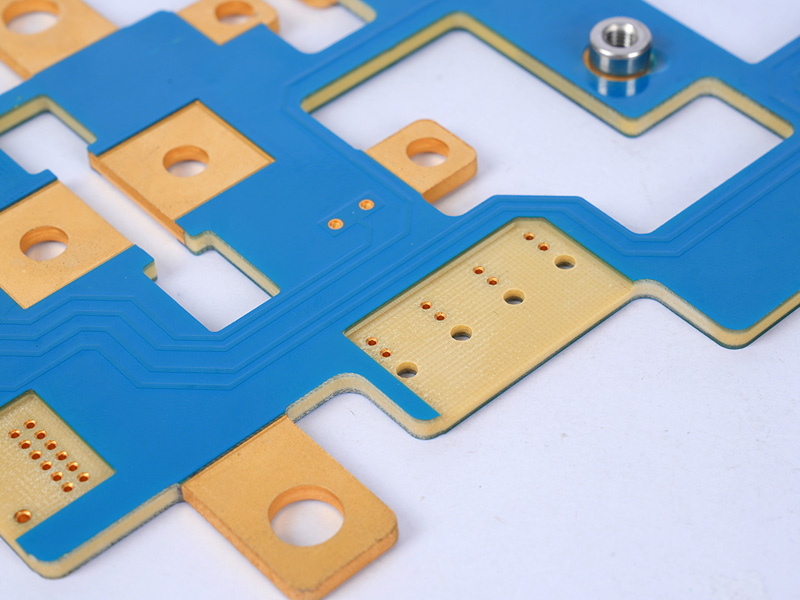
Copper Base PCB Vs Aluminum Base PCB: A Comparative Analysis
| Feature | Copper Base PCB | Aluminum Base PCB |
|---|---|---|
| Thermal Conductivity | Exceptionally high—ideal for high-power applications (100W+); copper core dissipates heat faster and more evenly | Moderate thermal conductivity; suitable for low-to-medium power applications (under 100W) |
| Electrical Conductivity | Superior electrical conductivity; minimal signal loss for high-speed and RF Copper Base PCB | Lower electrical conductivity; higher signal loss for high-speed applications |
| Durability & Strength | Higher mechanical strength; resistant to vibration and shock—perfect for aerospace and industrial equipment | Lightweight but lower mechanical strength; less suitable for heavy-duty industrial or aerospace use |
| Copper Thickness Flexibility | Customizable heavy copper thickness (including ultra-thick copper); tailored to exact power requirements | Limited metal thickness options; not ideal for heavy copper applications |
| Application Suitability | Medical imaging devices, aerospace avionics, high-power industrial machinery, RF equipment | Consumer electronics, low-power industrial devices, LED lighting, small-scale power electronics |
| Compliance Compatibility | Easy to manufacture to ISO 13485 (medical), AS9100D (aerospace), IATF 16949 (industrial) | Compliant for consumer and low-power industrial standards; less commonly used for medical/aerospace applications |
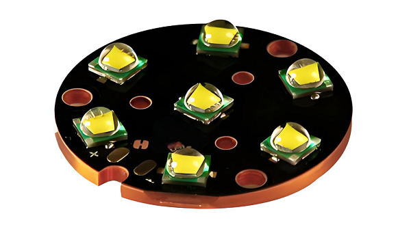
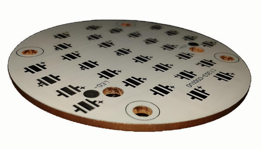
Copper Base PCB Applications In Medical, Aerospace & Industrial Sectors
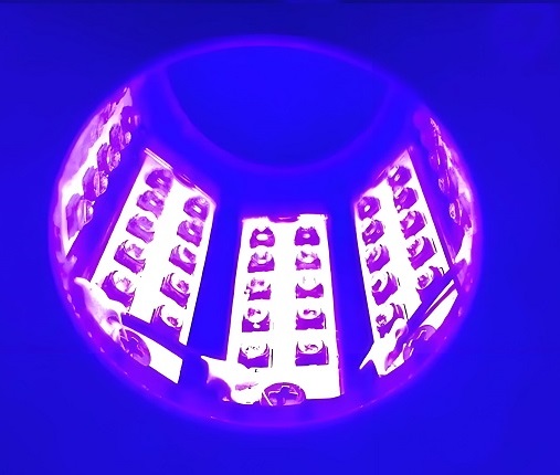
Copper Base PCB For Medical Equipment
Copper Base PCB is a critical component in high-power medical equipment, where thermal management and regulatory compliance are non-negotiable. EBest’s medical Copper Base PCB is integrated into medical imaging devices (CT scanners, MRI machines) and high-power diagnostic equipment, where the high thermal conductivity of copper core materials prevents overheating and ensures consistent, reliable performance. All our medical Copper Base PCB is manufactured to ISO 13485:2016 standards, meeting the strict quality and safety requirements of the medical industry, with precise impedance control to avoid signal interference in sensitive diagnostic equipment.
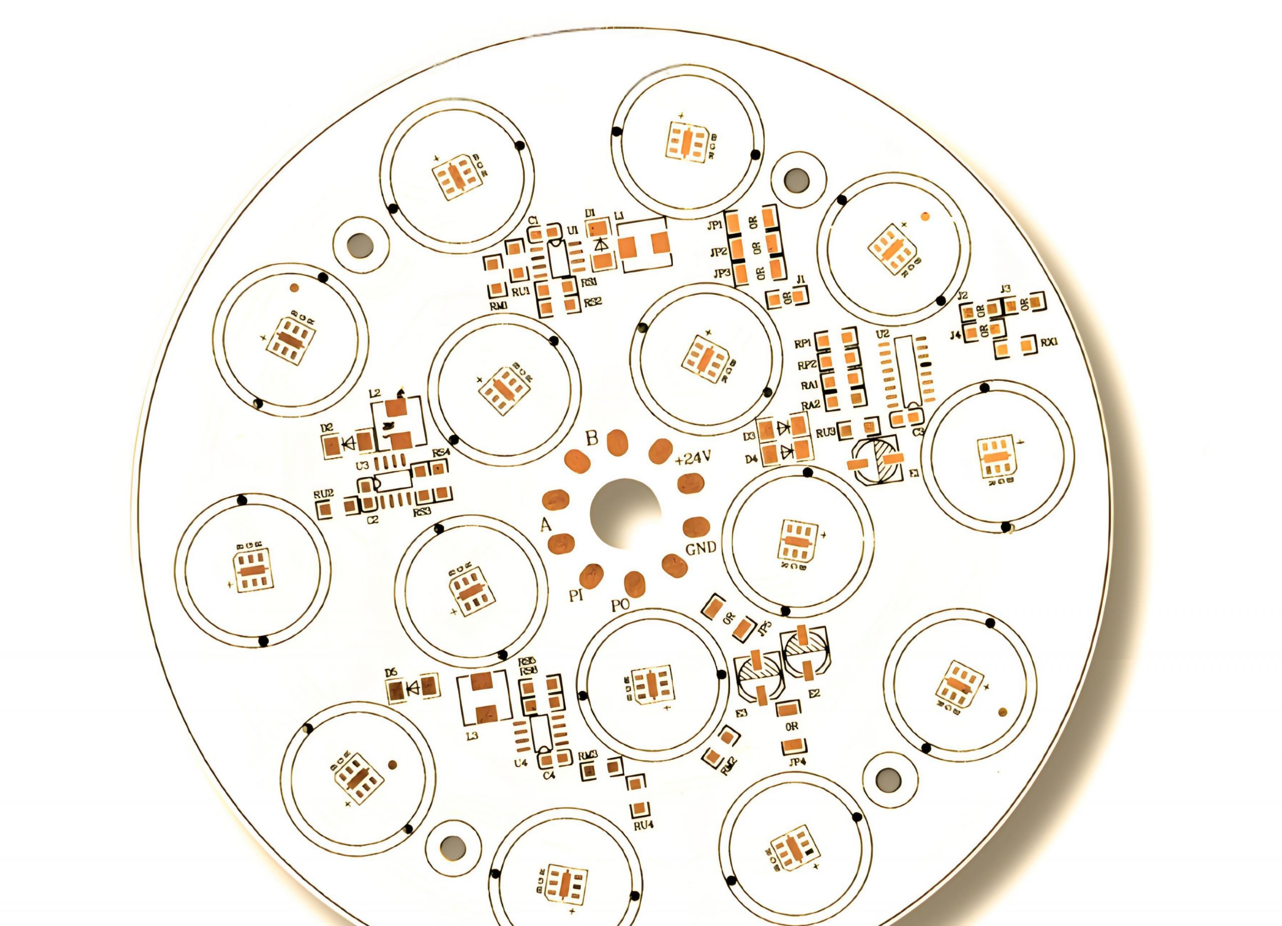
Copper Base PCB For Aerospace Systems
Aerospace avionics and flight systems demand Copper Base PCB that delivers high thermal conductivity, superior mechanical strength, and full compliance with AS9100D standards. EBest’s aerospace Copper Base PCB is used in satellite communication systems, aircraft avionics, and aerospace power modules—our custom copper thickness and rigid-flex design integration ensure the PCB can withstand the extreme vibration, shock, and temperature conditions of aerospace environments. The superior electrical conductivity of our Copper Base PCB also minimizes signal loss for high-speed RF and communication systems in aerospace applications.
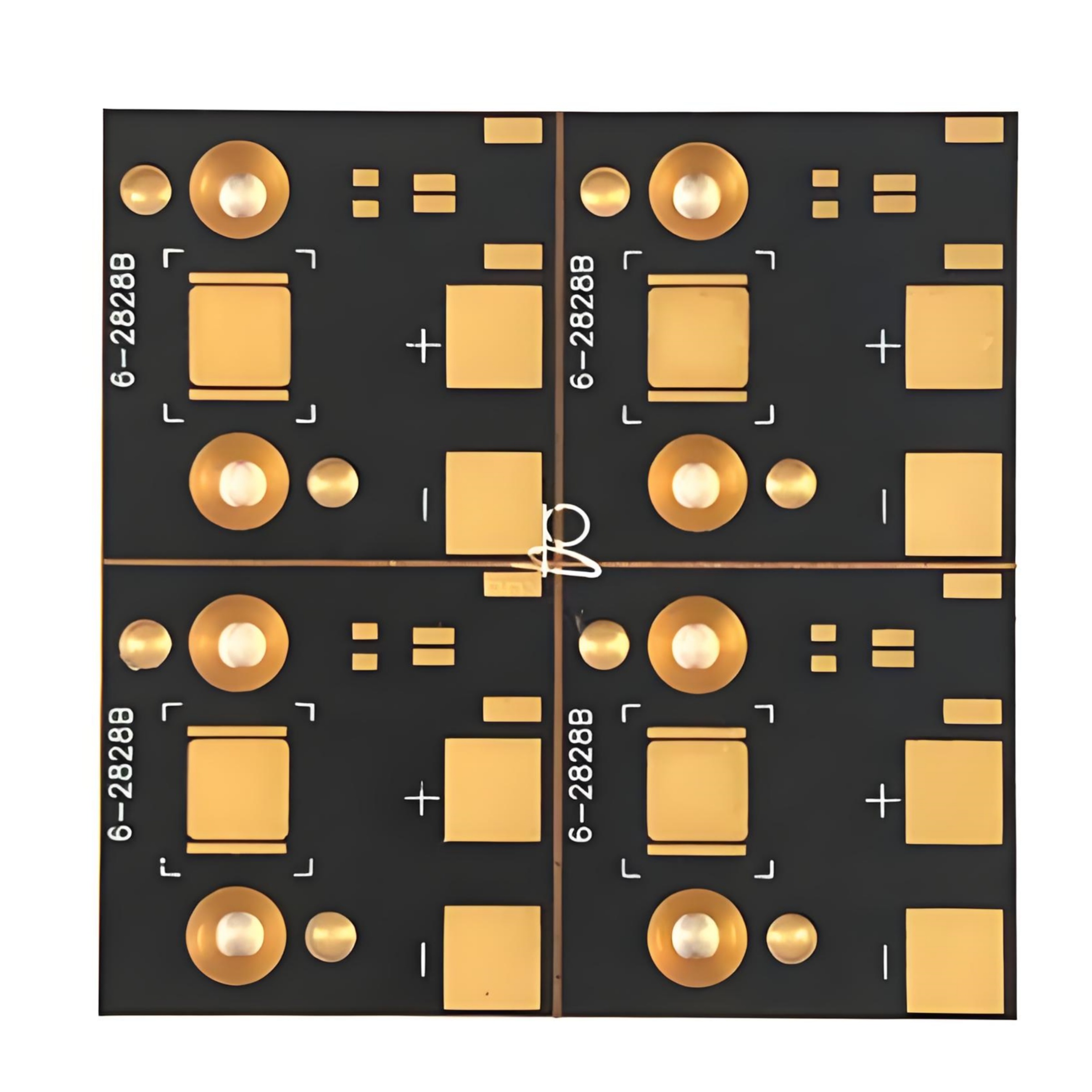
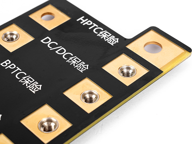
Copper Base PCB For Industrial Equipment
Heavy-duty industrial machinery (factory automation, power distribution, heavy manufacturing) relies on Copper Base PCB for high-power performance and long-term durability. EBest’s industrial Copper Base PCB is designed for IATF 16949 compliance, with heavy copper thickness and temperature-resistant materials to handle the high-power and harsh operating conditions of industrial equipment. Our Copper Base PCB for industrial use also features precise component placement and soldering, ensuring zero defects and reliable performance in 24/7 industrial operations.
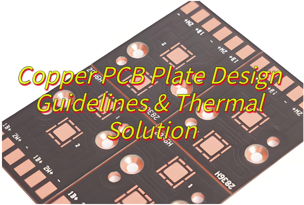
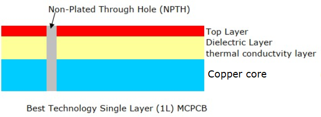
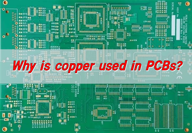
How To Optimize Thermal Conductivity For Copper Base PCB?
Optimizing thermal conductivity is the most critical step in Copper Base PCB design for high-power applications, and the solution lies in strategic material selection, copper core design, and board layout—with EBest’s engineering team following a proven, step-by-step process for maximum thermal performance. First, select a high-purity copper core material for your Copper Base PCB; high-purity copper has superior thermal conductivity compared to low-grade copper, ensuring faster and more efficient heat dissipation. Second, customize the copper thickness to match your exact power requirements—thicker copper cores dissipate more heat for high-power applications, and EBest offers flexible copper thickness options for every Copper Base PCB design. Third, design the Copper Base PCB layout with thermal vias placed strategically to transfer heat from the copper core to the board’s surface and heat sinks, eliminating hotspots that cause performance issues and component failure. Fourth, use thermal interface materials (TIMs) in conjunction with your Copper Base PCB to enhance heat transfer to external cooling systems, such as heat sinks or fans. EBest’s engineering team tests every Copper Base PCB design for thermal conductivity, using advanced thermal imaging technology to identify and eliminate hotspots before prototyping—ensuring your Copper Base PCB delivers optimal thermal performance for your specific application.
What Industry Certifications Do Copper Base PCB Require?
Copper Base PCB certifications vary by industry, and compliance is non-negotiable for medical, aerospace, and industrial applications—EBest manufactures all Copper Base PCB to the specific certifications required for your project, eliminating compliance risks and costly redesigns. For medical copper base PCB, the core certification is ISO 13485:2016, which sets strict quality management standards for medical devices and their components, ensuring uncompromising safety, reliability, and full traceability. For aerospace Copper Base PCB, AS9100D is the mandatory certification, covering the unique quality and performance requirements of aerospace systems, including resistance to extreme environmental conditions. For industrial Copper Base PCB, IATF 16949 and ISO 9001:2015 are the key certifications, setting global quality standards for automotive and general industrial equipment manufacturing. All EBest Copper Base PCB also complies with REACH, RoHS, and UL standards, ensuring environmental safety and electrical safety for global markets. Our manufacturing process is built around these certifications, with strict quality control checks at every stage of Copper Base PCB design, prototyping, and assembly to maintain full compliance at all times.
FAQ: Common Questions About Copper Base PCB Answered
Q1: What is the maximum copper thickness EBest offers for Copper Base PCB?
EBest offers fully customizable copper thickness for Copper Base PCB, from standard thin copper to ultra-heavy copper options—all tailored to the power and thermal requirements of your medical, aerospace, or industrial application. Our engineering team will recommend the optimal copper thickness for your Copper Base PCB design, balancing thermal conductivity, mechanical strength, and board flexibility for your specific use case.
Q2: Can EBest produce rigid-flex Copper Base PCB for custom applications?
Yes, EBest’s engineering team specializes in integrating rigid-flex design principles into Copper Base PCB manufacturing, producing custom rigid-flex copper core PCBs for aerospace and industrial applications that demand both flexibility and high thermal conductivity. Our rigid-flex Copper Base PCB is designed to meet the same industry certifications and performance standards as our standard copper core PCBs.
Q3: What lead times does EBest offer for Copper Base PCB mass production?
EBest’s standard lead times for Copper Base PCB mass production align with industry best practices, and we offer 24-hour expedite shipping for urgent orders—critical for time-sensitive medical, aerospace, and industrial projects. Our monthly production capacity of 260,000 square feet ensures we can scale production seamlessly to meet your large-batch Copper Base PCB needs with no delays.
Q4: Does EBest provide component sourcing for Copper Base PCB assembly?
Yes, as a one-stop Copper Base PCB provider, EBest offers full component sourcing for assembly, matching high-quality, industry-compliant components to your Copper Base PCB design’s power, performance, and compliance requirements. We source components from trusted global suppliers, ensuring perfect compatibility and long-term reliability for your medical, aerospace, or industrial project.
Q5: How does EBest test Copper Base PCB for thermal and electrical performance?
EBest uses advanced in-house testing technology to validate every Copper Base PCB’s thermal and electrical performance: thermal imaging for heat dissipation and hotspot detection, precision impedance testing for high-speed and RF copper core PCBs, and comprehensive electrical performance testing to ensure minimal signal loss and maximum power efficiency. All testing is completed before prototyping and mass production, to ensure your Copper Base PCB meets or exceeds your performance goals.
Q6: Is EBest’s Copper Base PCB compliant with global environmental standards?
Yes, all EBest Copper Base PCB is fully compliant with REACH and RoHS environmental standards, eliminating hazardous substances and ensuring your product can be sold in global markets without environmental compliance issues. Our manufacturing process also prioritizes sustainability, with waste reduction and eco-friendly production practices for all Copper Base PCB projects.
Q7: Can EBest create custom Copper Base PCB for low-volume, high-complexity projects?
Absolutely—EBest supports full customization for low-volume, high-complexity Copper Base PCB projects, including medical and aerospace applications that demand unique design and performance requirements. Our small-batch prototyping and production capabilities mean we can deliver high-quality, custom Copper Base PCB for low-volume projects with the same speed and compliance as large-scale production.
Q8: What post-production support does EBest offer for Copper Base PCB projects?
EBest provides comprehensive post-production support for all Copper Base PCB projects, including detailed performance testing feedback, expert assembly guidance, and ongoing technical support for your product development and production processes. Our team is available to answer any technical questions and provide tailored solutions for any Copper Base PCB performance or assembly issues you may encounter.
Order Your Custom Copper Base PCB From EBest Today
EBest is your trusted partner for Copper Base PCB design, prototyping, assembly, and mass production—offering one-stop custom solutions for the medical, aerospace, and industrial equipment industries. Our 20+ years of copper core expertise, industry-leading certifications, 24-hour expedite shipping, and personalized engineering support ensure your Copper Base PCB project is a success, from initial concept to final production. We manufacture all types of Copper Base PCB, including heavy copper, high TG, impedance control, and rigid-flex copper core PCBs, with full customization to match your unique performance, compliance, and production needs. Whether you need a small-batch prototype or large-scale mass production, EBest has the capacity, expertise, and uncompromising quality to deliver your Copper Base PCB on time and to the highest global industry standards. To order your custom Copper Base PCB or discuss your project requirements in detail, send an email to sales@bestpcbs.com—our team of dedicated PCB engineers will respond promptly and work with you to create the perfect copper core PCB solution for your business.