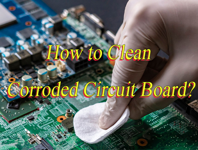
How to choose IT170GRA2 material? Let’s discover definition, datasheet, benefits, applicable frequency range, cost and alternative solution for IT-170GRA2.
Are you troubled with these questions?
How to prevent signal attenuation from material loss in high-frequency transmission?
How to manage heat in multi-layer PCBs while maintaining high-density routing efficiency?
How to shorten prototyping cycles for rapid design validation and market entry?
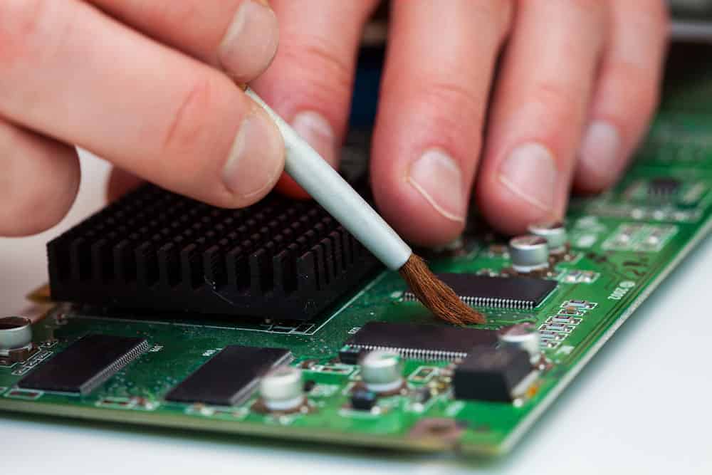
As a high speed PCB manufacturer, EBest Circuit (Best Technology) can provide you service and solution:
IT170GRA2 material delivers ultra-low loss with dissipation factor ≤0.002 at 10GHz, ensuring cleaner signal integrity and 30% higher first-pass design success.
Thermal conductivity ≥3.0W/m·K combined with optimized heat dissipation paths reduces board temperature rise by 15% in high-density designs, eliminating thermal stress risks.
48-hour rapid prototyping and direct material database access cut design iteration time in half, doubling speed-to-market for competitive edge.
Welcome to contact us if you have any request for high speed PCB: sales@bestpcbs.com.
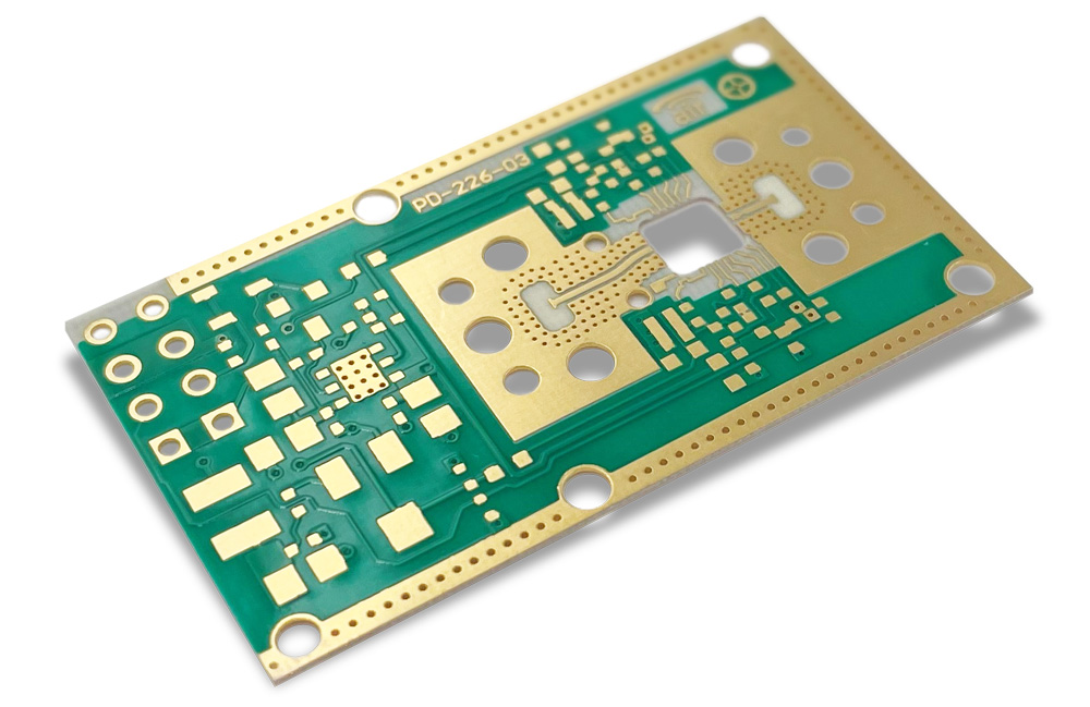
What Is IT170GRA2?
IT170GRA2is a high-performance copper-clad laminate (CCL) manufactured by ITEQ, specifically designed for high-speed and high-frequency printed circuit board (PCB) applications. The model name encodes its core features: “IT” stands for the brand ITEQ, “170” indicates a glass transition temperature (Tg) exceeding 170°C (verified at 175°C via DSC testing), “GR” denotes glass fiber reinforced substrate, “A” signifies a halogen-free environmental formulation (RoHS compliant), and “2” represents the second-generation optimized version.
Compared to its predecessor (e.g., IT-170GRA1), it achieves reduced dielectric loss (Df≈0.012) and enhanced anti-CAF (anti-ionic migration) performance. Defined as an epoxy resin/glass fiber cloth-based high Tg halogen-free CCL, it combines low signal loss, high thermal resistance (Tg=175°C), and high reliability, making it ideal for high-speed scenarios including 5G communication systems, server backplanes, and automotive electronic control units.
High-Frequency Signal Low-Loss Transmission: Df value 0.009–0.012 (@10GHz) reduces signal loss by approximately 40% compared to FR-4, ensuring signal integrity for 25Gbps+ high-speed links (e.g., PCIe 5.0) and minimizing data transmission errors.
Stable Performance in High-Temperature Environments: Tg=175°C supports lead-free soldering processes, Z-axis CTE of 45ppm/℃ minimizes interlayer separation, and passing 85°C/85%RH 1000h CAF test extends service life in high-temperature scenarios like 5G base stations and automotive electronics.
Environmentally Compliant and Safe: Halogen-free formulation meets RoHS/IEC 61249-2-21 standards, UL 94 V-0 flame retardancy enhances terminal product safety, complying with global environmental regulations.
High Process Compatibility and Cost Efficiency: Supports advanced processes like laser drilling and HDI stacking, copper foil peel strength ≥0.7N/mm prevents detachment during processing. Cost is 30%+ lower than ultra-low loss materials (e.g., Megtron 6), achieving 80% of FR-4 performance at 10–25GHz scenarios, balancing performance and cost.
Precise Impedance Control: Dk value 3.85±0.05 (@10GHz) maintains stable frequency variation, supports ±3% tolerance impedance design, avoids signal reflection issues, suitable for precision requirements like 100G optical modules in data centers.
Multi-Scenario Verified Reliability: 10GHz insertion loss ≤-0.8dB/inch in 5G base station RF front-end boards, 77GHz automotive radar withstands thermal cycling (-40°C~150°C) without delamination, 56G PAM4 eye diagram jitter <0.15UI in data centers, validated by real-world test data.
What Frequency Range Is IT-170GRA2 Suitable for?
The applicable frequency range of IT-170GRA2 is 10–25GHz, primarily covering mid-to-high frequency scenarios. Its optimal operating range is 10–25GHz, where dielectric loss Df is ≤0.012, ensuring controlled signal loss, for instance, insertion loss at 25GHz is approximately -1.75dB per inch. Beyond 25GHz, Df rises to 0.015–0.020, dielectric constant Dk fluctuates by more than ±0.1, leading to insertion loss exceeding -3dB per inch and impedance mismatch risks. For ultra-high frequency applications (such as 77GHz automotive radar or terahertz scenarios above 30GHz), it is unsuitable due to excessive loss and requires ultra-low loss materials like Megtron 7.
IT170GRA2 Material Selection Guide for High Speed PCB
1. Signal Rate Requirement Assessment
Determine if the signal rate is ≤56Gbps PAM4 (equivalent frequency ≤28GHz). For rates exceeding this standard, ultra-low loss materials like Panasonic Megtron 6 are required. For lower rates, proceed to temperature adaptability verification.
2. Operating Temperature Adaptability Verification
Confirm if long-term operating temperature is ≤130°C. For extreme environments exceeding 150°C (e.g., engine ECU), polyimide substrates must be used to ensure thermal stability. If temperature is ≤130°C, proceed to cost budget analysis.
3. Cost Budget Matching Analysis
Evaluate if the project budget can accommodate ≥1.5 times the cost of FR-4. For ultra-low-cost solutions, standard FR-4 remains viable. For mid-to-high costs, IT-170GRA2 is optimal due to its cost-effectiveness in the 10–25GHz frequency range.
4. Scenario-Based Parameter Configuration
Select recommended configurations based on application scenarios:
5G Base Station RF Board: Use 0.25–0.5mm thickness, HVLP low-roughness copper foil, and 2–6 layer symmetric stackup for 50Ω single-ended impedance ±3% control and fiber weave effect compensation.
PCIe 5.0 Interface Card: Adopt 0.8–1.2mm thickness, RTF reverse copper foil, and 8–12 layer hybrid stackup for 85Ω differential impedance ±2% accuracy and back-drilled stub ≤8mil.
100G Optical Module Substrate: Apply 0.15–0.3mm thin board, HVLP copper foil, and 4-layer thin design for 100Ω differential impedance ±3% and golden finger length optimization.
Automotive ADAS Controller: Utilize 1.5–2.0mm thickness, STD standard copper foil, and 6–8 layer high-Tg core for 90Ω differential impedance ±4% and enhanced thermal stress simulation.
5. Strict Avoidance of Prohibited Scenarios
Strictly prohibit the following four categories:
Continuous signal frequencies >25GHz (e.g., 77GHz automotive radar) due to excessive loss causing signal failure.
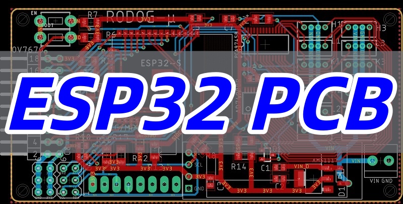
ESP32 PCB is the foundation of countless smart devices. This guide explores its design, features, and how a custom board can power your next IoT project.
Do you ever feel stalled bringing your brilliant IoT idea to life?
Complex Design Rules: The high-speed and wireless nature of the ESP32 makes circuit board layout tricky. A small error can ruin Wi-Fi or Bluetooth performance.
Component Sourcing Headaches: Finding genuine, high-quality components for your PCB can be difficult and time-consuming.
Signal Integrity Issues: Without careful planning, noise can disrupt the ESP32’s sensitive analog and radio functions.
Manufacturing Misunderstandings: Not knowing a manufacturer’s capabilities can lead to designs that are expensive or impossible to build.
Thermal Management Problems: Overheating can cause your device to crash or fail prematurely, especially in compact designs.
Fortunately, these challenges have complete solutions. Partnering with an experienced PCB manufacturer transforms these obstacles into a smooth path to a finished product.
Expert Layout Guidance: We assign engineers who understand RF (Radio Frequency) principles. They ensure your ESP32 PCB layout meets all critical design rules for optimal performance.
Reliable Supply Chain: We have established relationships with component suppliers. This guarantees we source authentic parts for your custom ESP32 PCB.
Advanced Design Analysis: Our team uses sophisticated tools to check for signal integrity problems before production. This proactive approach saves time and cost.
Design for Manufacturing (DFM) Check: We provide a free DFM review. We ensure your ESP32 PCB design is optimized for a smooth and cost-effective manufacturing process.
Thermal Solution Integration: We help design the board stack-up and copper layers to effectively dissipate heat, ensuring long-term reliability.
EBest Circuit (Best Technology) is a professional PCB manufacturer with deep expertise in IoT projects. Our team provides end-to-end support, from reviewing your ESP32 PCB schematic to delivering high-quality boards. Pls feel free to contact us at sales@bestpcbs.com to discuss your project.
What is ESP32 PCB?
If you’re moving beyond the prototyping stage, you need to understand what an ESP32 PCB truly is. It’s the critical transition from a generic development board to a specialized, functional product.
An ESP32 PCB is a custom-designed printed circuit board that transforms the raw ESP32 chip from a component into a complete, embedded system. Think of it this way:
The ESP32 Chip is the Brain. It’s a powerful microprocessor with Wi-Fi/Bluetooth.
The Custom PCB is the Body. It provides the skeleton, nervous system, and interfaces this brain needs to function in the real world.
While a dev board like the ESP32-DevKitC is a fantastic all-in-one toolbox for testing and learning, a custom PCB is a precision-engineered instrument designed for one specific task.
The Key Difference: Dev Board vs. Custom ESP32 PCB
Feature
Development Board (e.g., ESP32-DevKitC)
Custom ESP32 PCB
Purpose
Learning, Prototyping, General Use
Final Product, Mass Production
Size & Form
Large, fixed size with unused features
Compact, minimal, shaped for your product’s enclosure
Cost (at volume)
High per unit
Drastically lower per unit
Components
Includes everything, even what you don’t need
Only the essentials for your application
Optimization
Generic performance
Highly optimized for power, signal integrity, and thermal management
When we design a custom board, we’re building a complete ecosystem around the ESP32. Here’s what that actually includes:
Power Management Circuitry: This is not just a simple USB port. We design robust power regulation (like LDOs or DC-DC converters) to provide clean, stable voltage to the ESP32 and all peripherals, even from a noisy battery source.
Memory & Storage: We add the necessary Flash memory and PSRAM based on your firmware’s requirements, ensuring reliable operation without bloat.
The Antenna Ecosystem: This is a major differentiator. We integrate the antenna—either a PCB trace antenna, a ceramic chip antenna, or an u.FL connector for an external antenna—and design the matching network for optimal Wi-Fi/BT range.
Peripheral Interfaces: We break out the necessary GPIOs to dedicated headers or connectors for your specific sensors (I2C, SPI, ADC), actuators, displays, and other components.
Programming & Debugging: We include a compact, cost-effective programming interface (like a simple serial header) for factory flashing and future updates, unlike the bulky USB-to-Serial chip on dev boards.
In essence, a custom ESP32 PCB is the process of distilling a general-purpose prototype into a sleek, reliable, and cost-effective final product. It’s what allows your smart device to be manufactured efficiently and perform reliably in the field.
For a client, the decision to create a custom ESP32 PCB is the decision to professionalize your invention. It’s the key to reducing size, slashing costs, and ensuring the robust performance that customers expect. At EBest Circuit (Best Technology), we specialize in guiding you through this exact process, turning your proven concept into a manufacturable reality.
What are the Features of PCB ESP32?
The features of a PCB built for the ESP32 are what make it so powerful for IoT. They go far beyond just holding the chip.
Robust Power Design: A good board includes a stable voltage regulator. It ensures the ESP32 gets clean power even when the battery is low or input voltage fluctuates.
Optimized RF Layout: This is perhaps the most critical feature. The ESP32 PCB antenna design is carefully planned. Proper grounding and trace routing prevent interference. This gives you the best possible Wi-Fi and Bluetooth range.
Rich Connectivity Options: The PCB breaks out the ESP32’s many pins. This allows for easy connection to sensors, displays, and motors. You can find headers for I2C, SPI, UART, and GPIOs.
Efficient Thermal Management: The board itself helps cool the chip. Thermal vias and large copper pours pull heat away from the ESP32. This prevents overheating during intense tasks.
Compact Form Factor: A custom ESP32 PCB can be made very small. This is perfect for fitting into wearable devices or other space-constrained applications.
These features work together to create a reliable foundation for any connected device.
What’s Function of ESP32 on PCB?
The ESP32 chip on the PCB is the command center. Its job is to process information and make decisions.
First, it connects to the internet or other devices via its built-in Wi-Fi and Bluetooth.
Then, it reads data from sensors connected to the PCB, like a temperature sensor. After that, it processes this data.
Finally, it acts on it—for example, by sending a command to an actuator or transmitting the data to the cloud.
The ESP32 on PCB orchestrates all the electronic components around it. It turns a simple board into a smart, connected device.
What is an ESP32 Board Used for?
Understanding the applications of the ESP32 is the first step. The core strength of the ESP32—its low cost and wireless connectivity—is fully unlocked only when it’s packaged efficiently for its specific task. Let’s explore the common use cases, with a focus on what moving to a custom PCB makes possible.
The Dev Board Limitation: A generic dev board is too large and expensive to fit inside a standard light switch wall plate. It also includes unnecessary components, wasting space and money.
The Custom PCB Advantage: We design a compact, shape-optimized board that fits perfectly into the product’s enclosure. The design is optimized for low power consumption, allowing battery-powered sensors to last for years. This is where a robust ESP32 PCB layout for power efficiency is critical.
2. Industrial Monitoring & Control
Example Devices: Machine health monitors, environmental sensors (temperature, humidity, VOC), and asset trackers.
The Dev Board Limitation: Dev boards are not designed for harsh industrial environments. They are vulnerable to electrical noise, vibration, and temperature fluctuations, leading to crashes and data loss.
The Custom PCB Advantage: We can build ruggedized boards with conformal coating, robust power conditioning to handle noise, and secure mounting points. For an ESP32 drone PCB used in agricultural surveying, the board must be lightweight yet resilient to vibration. This level of reliability is impossible with a standard dev board.
3. Consumer Gadgets and Wearables
Example Devices: Fitness trackers, smart watches, and connected toys.
The Dev Board Limitation: A dev board is bulky, power-hungry, and aesthetically unworkable for a wearable device.
The Custom PCB Advantage: We can create tiny, flexible, or rigid-flex boards that contour to the wearable’s form factor. Power management is meticulously designed for maximum battery life. The ESP32 PCB antenna design is optimized to perform well even when close to the human body. This is a hallmark of professional ESP32 custom PCB design.
The Dev Board Limitation: These devices are often deployed in remote, outdoor locations. Dev boards lack the necessary weatherproofing and long-range connectivity options.
The Custom PCB Advantage: We can design boards with enclosures that are sealed against moisture and dust. The RF layout can be optimized for a specific antenna (e.g., a high-gain external antenna) to maximize the wireless range in open fields, a key consideration in any ESP32 PCB design guide.
5. High-Performance Hobbyist Projects
Example Devices: The WLED ESP32 PCB for complex LED arrays, the ESP32 marauder PCB for wireless security testing, or the ESP32 cam PCB for high-quality video streaming.
The Dev Board Limitation: While hobbyists start with dev boards, advanced projects demand custom PCBs to integrate specialized components, improve signal integrity for video streams, or create a professional-looking final product.
The Custom PCB Advantage: We help hobbyists and prosumers bridge the gap to a polished product. A custom PCB with ESP32 allows for the perfect integration of all components, resulting in better performance and a more marketable end-unit.
The shift from a standard ESP32 board to a custom ESP32 PCB is the shift from “it works” to “it works perfectly in its intended environment.” It’s about optimizing for:
Cost at volume
Size and Form Factor
Power Consumption
Reliability and Ruggedness
Performance (RF range, signal integrity)
At EBest Circuit (Best Technology), we don’t just manufacture your PCB; we help you identify these optimization points. We use our expertise to ensure your ESP32 PCB schematic and layout are tailored for your application’s unique challenges, turning a great idea into a viable, manufacturable product.
ESP32 PCB Footprint Best Practices
The footprint is the pattern of copper pads on the PCB where the ESP32 chip is soldered. Getting this right is non-negotiable. A bad footprint can lead to poor soldering and device failure.
Follow the Datasheet: Always use the official ESP32 PCB footprint from Espressif’s datasheet. Do not try to create it from scratch. This ensures the pad sizes and spacing are perfect.
Use Correct Solder Mask: The solder mask should have a tight opening around the pads. This prevents solder from bleeding and creating short circuits during assembly.
Include a Courtyard: Add a keep-out area around the footprint. This ensures no other components are placed too close, which helps with soldering and inspection.
Thermal Pad Design: Many ESP32 modules have a large thermal pad underneath. The footprint must have a corresponding pad with multiple vias. This helps transfer heat into the ground plane of the PCB.
Reference Designator: Clearly label the footprint on the silkscreen. This helps during assembly and any future debugging.
Using a library like ESP32 PCB KiCad or ESP32 PCB design EasyEDA can help. These often include pre-verified footprints. This saves time and prevents errors.
Where to Get PCB for ESP32?
Navigating the path from an ESP32-based idea to a functional printed circuit board (PCB) can be complex. The right sourcing strategy depends heavily on your project’s stage, volume, and performance requirements. This guide breaks down the options, highlighting why a partnership with a specialist manufacturer like EBest Circuit (Best Technology) is crucial for moving beyond the prototyping phase into successful mass production.
1. For Prototyping: Pre-made Development Boards
The fastest way to start developing with the ESP32 is to use a pre-assembled development board (e.g., from SparkFun or Adafruit). These are excellent for software development, proof-of-concept testing, and small-scale projects. However, they are often larger, more expensive per unit, and may include features unnecessary for your final product, making them unsuitable for commercial volume production.
2. For Custom Products & Commercialization: Custom PCB Manufacturing with EBest Circuit (Best Technology)
When you’re ready to productize your design, you need a custom PCB. This involves two critical steps:
Design: You create the schematic and layout using ECAD software. Open-source platforms like ESP32 PCB GitHub repositories can offer valuable reference designs.
Fabrication: You send your design files (Gerbers) to a PCB manufacturer. This is where the choice of partner becomes paramount.
While online “board houses” offer low-cost prototyping, they often lack the specialized expertise for a successful, high-performance ESP32 product. For a reliable, wireless-enabled device, you need a manufacturer with specific capabilities in impedance control, RF layout, and signal integrity—this is where EBest Circuit (Best Technology) excels.
EBest Circuit (Best Technology) bridges the gap between a basic design and a high-performance product. We don’t just manufacture your board; we provide expert Design for Manufacturability (DFM) analysis, ensuring your ESP32 PCB schematic and layout are optimized for reliability and performance from the start. Our support throughout the process de-risks your journey from concept to a finished, market-ready ESP32 PCB board.
Our specific capabilities for ESP32 PCBs include:
Advanced RF and Manufacturing Expertise: ESP32 designs demand precise control over impedance and RF characteristics. Our manufacturing processes are equipped to handle these requirements, ensuring stable wireless performance. We support complex multi-layer boards (up to 32 layers) which are often necessary for sophisticated ESP32-based products that integrate numerous functionalities.
Precision Engineering for High Density: We achieve fine line widths and spacing, with capabilities for outer layer lines down to 3.5/4 mil and inner layers down to 3/3 mil. This precision is essential for routing the dense BGA packages of modern ESP32 modules and maintaining signal integrity for high-speed interfaces like USB OTG on the ESP32-S3.
Comprehensive Surface Treatment Options: To ensure the best solderability and long-term reliability for your ESP32 board, we offer a variety of surface finishes suitable for RF applications, including ENIG (Immersion Gold), OSP, and Immersion Silver. We advise against HASL (Hot Air Solder Leveling) for fine-pitch ESP32 designs due to potential flatness issues.
Rigorous Quality Control: We adhere to strict quality standards, performing electrical testing to verify 100% connectivity (using either flying probe for prototypes or test fixtures for mass production) and inspecting against IPC-A-600 class 2/3 acceptance criteria to guarantee a reliable final product.
By leveraging our extensive manufacturing experience and technical capabilities, EBest Circuit (Best Technology) is the ideal partner to transform your ESP32 design into a robust, high-performance reality.
Designing a PCB for a high-speed, wireless module like the ESP32 demands precision engineering. EBest Circuit (Best Technology) possesses the advanced technical infrastructure and expertise to meet these stringent requirements.
1. Support for Complex Designs and Tools: We are agnostic to your design environment, seamlessly handling files from all major ECAD software, including designs made with ESP32 PCB layout Proteus. Our engineers are adept at working with your design files to ensure a smooth transition to production.
2. Critical High-Frequency and RF Expertise: The core of a successful ESP32 design lies in its radio frequency (RF) performance. Our capabilities are tailored for this challenge:
Advanced Layer Counts: We can manufacture boards with up to 12 layers, essential for complex products requiring dense component placement and multiple power domains while maintaining signal integrity.
Impedance Control: We strictly control impedance for high-speed data lines (like those for ESP32-S3’s USB OTG) to prevent signal reflection and data corruption. Our process controls impedance tolerance within ±10%, which is critical for stability.
ESP32 PCB Antenna Design: This is a critical differentiator. We expertly manage the antenna layout, ensuring optimal placement away from noise sources and proper grounding to maximize wireless range and connectivity reliability. Our ESP32 PCB design guide incorporates best practices for antenna matching circuits and keep-out areas.
3. Precision Manufacturing and Quality Assurance: Our manufacturing prowess, as detailed in our capability charts, ensures the highest quality:
Fine Line Technology: We achieve inner layer line widths/spacing down to 2.5/2.5 mil and outer layer down to 3/3 mil, allowing for dense and efficient layouts.
Diverse Materials: We work with standard FR-4 as well as high-speed/low-loss materials (e.g., TU-872SLK, IT-968) suitable for demanding RF applications, ensuring minimal signal loss (Df).
Rigorous Testing: Every board undergoes electrical testing for shorts and opens (E-test). We offer both flying probe for prototypes and test fixture testing for volume production, guaranteeing 100% functionality before shipment.
By leveraging these capabilities, we transform your custom ESP32 PCB design into a robust, high-performance reality, fully compliant with IPC standards.
Case of ESP32 Drone PCB Manufacturing at EBest Circuit (Best Technology)
This project showcases EBest Circuit (Best Technology)’s expertise in manufacturing a high-complexity, 8-layer rigid-flex PCB for a cutting-edge industrial inspection drone.
Application Scenario
The board serves as the core flight controller. Based on the ESP32-S3, it required robust wireless communication for real-time telemetry and HD video transmission. The rigid-flex design was critical: the rigid sections house the main processor and sensitive sensors, while the flexible portions allow the board to conform to the drone’s compact, irregular airframe, ensuring reliability under extreme vibration and EMI conditions.
PCB Specifications & Key Parameters
The board was built to the following precise specifications, demonstrating our manufacturing capabilities:
This project leveraged several of our advanced technical competencies:
Rigid-Flex Lamination Expertise: Precise control during the lamination process was essential to bond the rigid and flexible materials seamlessly without delamination.
Impedance Control & Signal Integrity: Our engineers meticulously controlled the impedance for the high-speed signals from the ESP32-S3, including the Wi-Fi RF lines and USB OTG differential pairs, ensuring stable data transmission.
Advanced Drilling & Plating: Achieving reliable PTH vias in the rigid-flex interface requires specialized drilling and plating techniques to ensure connectivity and mechanical strength.
Via-in-Pad and Resin Filling: This process was critical for the fine-pitch BGA components, creating a flat surface for soldering and enhancing reliability.
In conclusion, the ESP32 PCB is the unsung hero of the IoT revolution, providing the solid foundation upon which smart devices are built. This article has explored its design, function, and the immense potential of creating a custom board.
EBest Circuit (Best Technology) has the technical expertise and manufacturing precision to deliver high-quality ESP32 PCBs that perform. We help you navigate the complexities of RF design and thermal management. Pls feel free to send us your design files or questions anytime. Contact our team at sales@bestpcbs.com. We are here to help.
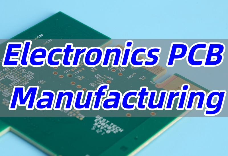
Electronics PCB manufacturing is the lifeblood of modern technology. This guide explores its types, quality control, and how to choose a top partner like EBest Circuit (Best Technology) for reliable, high-performance circuit boards.
What are the typical pain points companies face when sourcing PCBs?
Unreliable Quality: Boards failing after a short period of use.
Inconsistent Delivery Times: Unpredictable production schedules.
Poor Communication: Slow responses and lack of technical support.
Hidden Costs: Surprising charges that appear after ordering.
Limited Technical Capability: Manufacturers unable to handle complex designs.
Fortunately, these problems are entirely avoidable. The solutions provided by EBest Circuit (Best Technology) directly address these concerns:
Rigorous Quality Control: We implement a multi-stage inspection system. Every electronic PCB board manufacturer process is monitored to ensure zero defects.
Structured Production Planning: Our advanced planning ensures on-time delivery. We keep your projects moving smoothly.
Dedicated Engineering Support: You get a single point of contact. Our team provides proactive updates and expert advice.
Transparent Quoting: We provide clear, upfront pricing. There are no surprises, helping you manage your electronics PCB manufacturing cost effectively.
Advanced Technical Expertise: Our factory is equipped for sophisticated projects. We specialize in complex multilayer PCB manufacturing process.
For over 19 years, EBest Circuit (Best Technology) has been a trusted PCB and flexible circuit solutions provider, turning complex requirements into high quality electronic boards. Our expertise is proven by advanced capabilities in manufacturing high-layer counts up to 32 layers, handling extreme copper weights from 1oz to 20oz, and achieving precise features like 3/3 mil line spacing and 0.1mm micro-vias. For a expert consultation, reach us at sales@bestpcbs.com.
Why Electronics PCB Manufacturing Is Critical for Modern Devices?
At the heart of every modern electronic device lies its printed circuit board (PCB). More than just a platform for components, the PCB is the central nervous system of your product, determining its performance, reliability, and longevity. The choice of your PCB manufacturer is therefore not a simple procurement step; it is a strategic engineering decision.
From Design to Better Quality Electronic PCBs:
A design file is a perfect, theoretical model. Transforming it into a high-functioning physical board is where professional manufacturing makes the critical difference. This process hinges on several key capabilities:
Signal Integrity & Material Science: High-speed digital and high-frequency RF designs (like those in 5G and IoT devices) demand precise control over electrical signals. Professional manufacturers achieve this through expertise in selecting specialized materials (like Rogers or Isola laminates) and controlling impedance with tolerances as tight as ±10%. Amateur fabrication can lead to signal loss, crosstalk, and data corruption.
Power Integrity & Thermal Management: Modern processors and ASICs require stable, clean power. This is ensured through sophisticated multilayer stack-ups with dedicated power and ground planes. Furthermore, effective thermal management via thermal vias and appropriate copper weights (e.g., 2oz for power circuits) prevents overheating, ensuring device stability and a longer lifespan.
Miniaturization and Reliability (HDI): As devices shrink and become more powerful, High-Density Interconnect (HDI) technology is essential. This involves advanced processes like laser-drilled micro-vias (as small as 0.1mm), stacked vias, and fine-line etching (3/3 mil line/space). These techniques allow for more functionality in a smaller footprint, which is critical for wearables, medical implants, and advanced consumer electronics.
In non-critical applications, a PCB failure might mean an inconvenience. However, in several advanced industries, the stakes are significantly higher:
Automotive: PCBs must withstand extreme temperatures, constant vibration, and humidity. They are the backbone of safety systems like ABS and airbag control units. Failure is not an option.
Medical: Devices for diagnostics and patient monitoring require absolute reliability. They often need to be biocompatible and manufactured in certified cleanrooms to ISO 13485 standards.
Aerospace & Defense: Boards must perform flawlessly under intense stress and in harsh environments, adhering to stringent standards like IPC-A-610 Class 3.
Choosing EBest Circuit (Best Technology) means partnering with experts who translate your complex designs into reliable, high-performance hardware. We bring over 19 years of focused expertise in advanced PCB and flexible circuit manufacturing. Ready to discuss how our manufacturing capabilities can bring robustness and reliability to your next project? Contact our engineering team at sales@bestpcbs.com for a consultation.
What are the Types of Electronics PCB Manufacturing?
Selecting the appropriate PCB type is a foundational engineering decision that directly impacts the performance, reliability, and cost of an electronic device. Moving beyond basic definitions, a deeper understanding of the classifications and their manufacturing implications is crucial. Here is a detailed breakdown based on industry standards and advanced fabrication capabilities.
1. Classification by Layer Count and Structure
This is the primary way to categorize PCBs, reflecting their complexity.
Single-Sided PCBs: Featuring a single conductive copper layer on one side of a substrate, these are the most straightforward to manufacture. They are cost-effective and ideal for simple, low-density circuits but offer limited functionality for modern devices.
Double-Sided PCBs: These boards have conductive layers on both the top and bottom surfaces, connected by Plated Through-Holes (PTH). This doubles the available area for components and routing, making them a versatile and common choice for a wide range of applications, from industrial controls to consumer electronics.
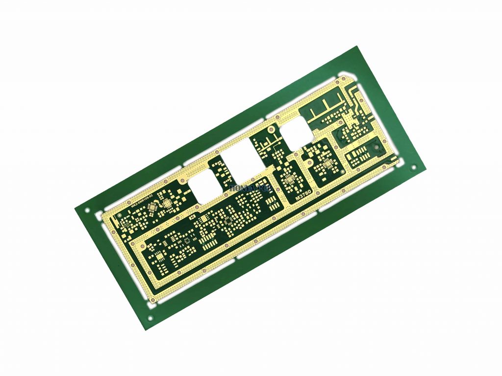
Multilayer PCBs: Defined as having three or more conductive layers, these boards are essential for complex, high-speed electronics. Layers are laminated together with insulating prepreg (PP) under high temperature and pressure.
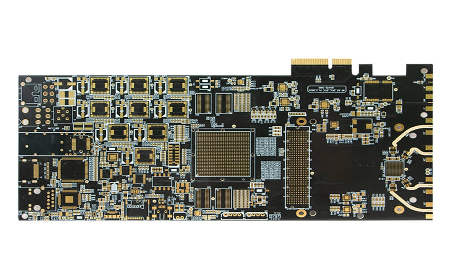
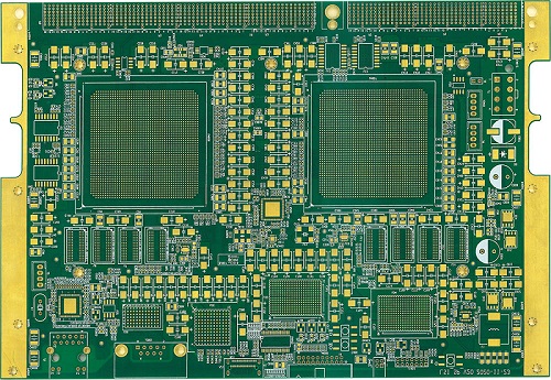
Capability Spotlight: Modern manufacturing, as detailed in your materials, can produce boards with up to 32 layers. High-TG (Glass Transition Temperature) materials, such as KB6167 or IT180, are often mandatory for boards exceeding 8 layers to ensure stability during the lamination process and under operational heat. The picture below is an 8-layer board for your reference.
2. Classification by Physical Properties: Rigidity and Flexibility
The base material defines the physical form of the board, enabling innovative product designs.
Rigid PCBs: The most common type, built on inflexible substrates like FR-4. They provide excellent mechanical support and are used in the vast majority of electronic equipment where the board does not need to move or bend.
Flexible PCBs (FPC): Manufactured on flexible plastic substrates like polyimide. Their key advantages include high flexibility, light weight, and excellent resistance to heat and vibration. They are perfect for dynamic applications or tight spaces, such as in cameras, wearable devices, and within automotive assemblies.
Rigid-Flex PCBs: This advanced hybrid integrates rigid boards for component support with flexible interconnects into a single structure. This combination simplifies the overall assembly, enhances reliability by eliminating the need for connectors between rigid boards, and allows for more compact, three-dimensional packaging.
3. Classification by Surface Finish
The surface finish is a critical quality factor, protecting the copper from oxidation and ensuring solderability. Your document lists an extensive portfolio, including:
HASL (Hot Air Solder Leveling): A common, cost-effective finish for general purposes.
ENIG (Electroless Nickel Immersion Gold): Provides a flat surface, excellent for fine-pitch components and offering good oxidation resistance.
Immersion Silver/Tin: Offers good performance for a range of applications.
ENEPIG (Electroless Nickel Electroless Palladium Immersion Gold): A premium finish with superior wire-bonding capability and resistance to corrosion.
Gold Finger Plating: Used for edge connectors, requiring a hard, durable gold plating. Combinations like HASL + Gold Finger or ENIG + OSP are also standard offerings to meet specific zone-specific requirements on a single board.
4. Classification by Specialized Material Properties
For high-performance applications, the base laminate material is specially engineered.
High-Frequency/High-Speed PCBs: These use specialized laminates (e.g., Rogers, Taconic) with controlled dielectric constants (Dk) and dissipation factors (Df) to maintain signal integrity at high frequencies, which is critical for 5G, radar, and satellite communications.
Metal-Clad PCBs (MCPCB): Designed for superior thermal management. They feature a metal base (typically aluminum or copper) that draws heat away from critical components, making them ideal for high-power LED lighting, power supplies, and automotive systems.
Ceramic PCBs: Offer exceptional thermal conductivity, electrical insulation, and stability in high-temperature environments, used in high-power modules and aerospace applications.
5. Classification by Via Technology
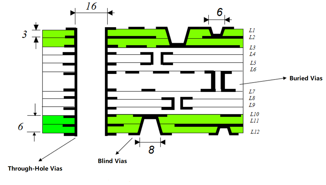
The method of creating connections between layers is a key differentiator in advanced PCB manufacturing.
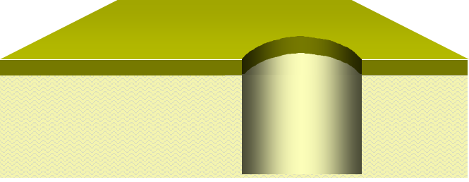
Through-Hole Vias: Standard vias drilled through the entire board.
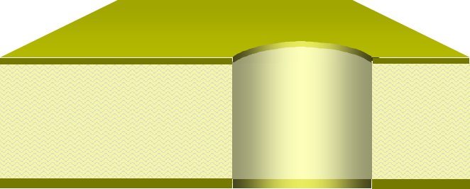
Blind Vias: Connect an outer layer to one or more inner layers, but do not go through the entire board.
Buried Vias: Connect internal layers without reaching the outer surfaces.
Microvias: These are small vias (typically with a diameter of 0.1mm or less) created by laser drilling. They are a cornerstone of HDI (High-Density Interconnect) technology, allowing for much higher wiring density and are essential for compact devices like smartphones.
In conclusion, the choice of PCB type is a strategic decision intertwined with your product’s electrical, thermal, and mechanical requirements. Partnering with a manufacturer like BEST Technology, which possesses the expertise across this full spectrum—from standard FR-4 to complex HDI and rigid-flex boards—ensures that your design is built on a foundation of reliability and performance.
How EBest Circuit (Best Technology) Excels in Electronics PCB Manufacturing for Global Clients?
In a competitive global market, excellence is not an accident. It is the result of a systematic commitment to quality, service, and innovation. EBest Circuit (Best Technology) stands out by focusing on what truly matters to our clients.
First, our quality control is uncompromising. We employ Statistical Process Control (SPC) at key stages. Our MES (Manufacturing Execution System) provides full traceability. You can trace every board back to its production batch. This is critical for quality assurance and continuous improvement.
Second, we provide unparalleled engineering support. Our team doesn’t just build your design; we partner with you to optimize it. We offer Design for Manufacturability (DFM) feedback. This helps prevent potential issues before production begins. It saves you time and reduces the cost of PCB manufacturing.
Third, we understand the importance of cost-efficiency. By optimizing our processes and maintaining strong supplier relationships, we offer highly competitive pricing without sacrificing quality. We give you clear insights into your electronics PCB manufacturing cost.
Finally, our customer service is proactive and responsive. We assign a dedicated project manager to your account. You will receive regular updates, ensuring you are always informed. This level of service builds trust and long-term partnerships.
Technical Capability for Electronic PCB Manufacturer
As a leading specialist in PCB fabrication, EBest Circuit (Best Technology) possesses extensive manufacturing capabilities to meet the demanding requirements of various industries, from consumer electronics to high-reliability automotive and telecommunications applications. Our technical prowess is detailed below, demonstrating our commitment to precision, quality, and innovation.
1. Materials We support a comprehensive range of substrate materials to cater to diverse electrical and thermal performance needs:
FR-4 Series: Standard TG (130-140°C), Mid TG (150°C), and High TG (170-180°C). We utilize premium brands like KB, Shengyi, and ITEQ, including halogen-free options.
High CTI Materials: Such as Shengyi S1600L for enhanced comparative tracking index.
High-Speed/Low-Loss Materials: Capable of processing mid-loss (e.g., IT-968, TU-883), low-loss (e.g., IT-958, TU-872SLK), and ultra-low-loss (e.g., IT-933, TU-993) laminates, including Isola products.
High-Frequency Materials: Expertise in ceramic-filled (e.g., Rogers 4350B, 4003) and PTFE-based (e.g., Rogers, Taconic, Arlon) materials for RF and microwave applications.
2. Layer Count We manufacture printed circuit boards with a wide range of complexity:
Standard Capability: 1 to 50 layers.
Advanced Capability: Up to 100 layers (subject to technical review for boards exceeding 50 layers).
3. Board Thickness We offer flexibility in board thickness with tight control over tolerances:
Standard Range: 0.4mm to 6.0mm.
Advanced Range: 0.15mm to 10.0mm.
Thickness Tolerance: ±0.1mm for boards ≤1.0mm; ±10% for boards >1.0mm. Tighter special tolerances are available upon request.
4. Surface Finish A variety of surface finishes are available to ensure solderability and end-use performance:
15. Metal Core PCBs (MCPCB) We specialize in manufacturing Aluminum and Copper-based PCBs for superior thermal management:
Layer Count: 1 to 6 layers (>6 layers subject to review).
Board Thickness: 0.5mm to 5.0mm.
Copper Thickness: 0.5 oz to 3 oz (>3 oz subject to review).
Thermal Conductivity: Supports materials with conductivity from 0.3 W/m·K to 6.0 W/m·K (Standard), and up to 12 W/m·K (Advanced).
Metal Base Thickness: 0.5mm to 5.0mm.
This overview underscores EBest Circuit (Best Technology)’s capacity to deliver high-quality, reliable PCBs tailored to your specific design requirements. Our engineering team is available for consultation to ensure your project’s success.
Multilayer PCB Manufacturing Process – EBest Circuit (Best Technology)
Transforming a complex circuit design into a reliable, high-performance multilayer Printed Circuit Board (PCB) is a feat of precision engineering. At EBest Circuit (Best Technology), our process for manufacturing boards from 4 to over 24 layers is built upon rigorous control and advanced capabilities at every stage. The following outline details the critical steps that ensure the integrity of your product’s foundation.
Phase 1: Inner Layer Fabrication – Creating the Internal Circuitry
This phase focuses on manufacturing the individual conductive layers that will be laminated inside the board.
Step 1: Panel Preparation (Board Cut)
Large sheets of copper-clad laminate (CCL) are precision-cut into smaller, standardized production panels. The primary goal is to maximize material utilization while meeting the design’s dimensional requirements.
Step 2: Inner Layer Imaging (Pattern Transfer)
Cleaning and Dry Film Lamination: The panel surface is thoroughly cleaned and then coated with a light-sensitive dry film.
Exposure: Ultraviolet light is projected through a photographic film (phototool) containing the circuit pattern onto the dry film, hardening the exposed areas.
Development: The unhardened dry film is chemically dissolved, revealing the copper that is not part of the desired circuit.
Etching and Stripping: The exposed copper is etched away. The remaining hardened dry film is then stripped off, leaving behind the precise copper circuitry.
Each inner layer is automatically scanned to detect any defects, such as shorts or opens. The layer then undergoes an oxide treatment (browning) to improve adhesion during the lamination process.
Phase 2: Layer Stack-Up and Lamination – Building the Multilayer Structure
The individual layers are assembled and bonded into a single, solid board.
Step 4: Lay-Up
The inner layers, sheets of insulating prepreg (B-stage epoxy resin), and outer layer copper foil are meticulously aligned and stacked in a specific sequence.
Step 5: Lamination Press
The stack is subjected to high temperature (approximately 200°C) and pressure in a hydraulic press. This causes the prepreg resin to melt, flow, and permanently cure, bonding the layers together. A controlled cooling cycle under pressure is critical to prevent warping.
Phase 3: Drilling and Plating – Establishing Interlayer Connections
Holes are drilled and metallized to create electrical pathways between the different layers of the board.
Step 6: Precision Drilling
Using Computer-Numerical Control (CNC) machines, holes for vias and component leads are drilled. We support a wide range of drill bit sizes, from 0.15mm for microvias to 6.5mm for larger tooling holes. For high-density designs, we utilize advanced laser drilling.
This is a critical chemical process. It begins with desmear to remove epoxy residue from the drilled hole walls. The panel then undergoes a series of baths that deposit a thin, conductive layer of copper (typically 1-3µm) onto the entire panel surface, including the hole walls, making them electrically conductive.
Phase 4: Outer Layer Formation – Completing the Circuit
The outer layers are patterned and plated to finalize the board’s circuitry.
Step 8: Panel Electrolytic Plating
The panel is plated with copper to increase the thickness of the conductive layer on the surface and within the holes, ensuring robust electrical connections.
Step 9: Outer Layer Imaging & Pattern Plating
A dry film is applied, exposed (often using high-precision Laser Direct Imaging – LDI), and developed to define the outer layer circuit pattern.
The panel is plated again with copper to build up the traces and pads, followed by a layer of tin, which acts as an etch resist.
Step 10: Etching (Strip-Etch-Strip)
The dry film is stripped away. The underlying copper is then etched, but the tin-plated circuits are protected. Finally, the tin is stripped, revealing the final, precise outer layer circuits.
Phase 5: Solder Mask and Surface Finish – Application and Protection
The board is prepared for component assembly.
Step 11: Solder Mask Application
A liquid photoimageable solder mask ink (typically green, but other colors are available) is applied to the panel. It is then exposed and developed to open windows over the solderable pads, protecting the copper circuitry from oxidation and preventing solder bridges.
Step 12: Surface Finish Application
A final coating is applied to the exposed copper pads to ensure reliable solderability. We offer a wide range of finishes, including HASL (Lead-free), ENIG (Electroless Nickel Immersion Gold), Immersion Silver, Immersion Tin, and ENEPIG (Electroless Nickel Electroless Palladium Immersion Gold).
Step 13: Legend Printing (Silkscreen)
Component designators, logos, and other markings are printed onto the board surface using epoxy ink, typically in white.
Phase 6: Final Fabrication, Testing, and Inspection
The individual boards are separated and subjected to final quality assurance.
Step 14: Profiling (Routing)
The individual PCBs are routed out of the production panel using CNC milling machines, V-scoring, or laser cutting.
Step 15: Electrical Testing
Every board undergoes 100% electrical testing. Flying Probe testers are used for prototypes and small batches, while custom test fixtures are employed for high-volume production to verify electrical continuity and isolation.
Step 16: Final Quality Control (FQC) & Packaging
A comprehensive visual and dimensional inspection is performed. Approved boards are then cleaned, vacuum-sealed, and packaged to prevent moisture absorption and damage during shipping.
By meticulously controlling each of these stages, EBest Circuit (Best Technology) ensures that every multilayer PCB delivers the performance, reliability, and durability required for advanced electronic applications.
How to Ensure Quality When Proceeding Electronic Circuit Board Manufacturing?
Quality is not just a final inspection; it is built into every step. At EBest Circuit (Best Technology), our quality assurance system is multi-layered.
Automated Optical Inspection (AOI): This machine scans the boards after solder paste printing and component placement. It catches any missing or misaligned parts instantly.
In-Circuit Test (ICT): This is a powerful test that checks the electrical performance of the board. It verifies that every component is the correct value and is properly connected.
Flying Probe Test: For smaller batches, flying probe testers provide a flexible and efficient electrical test solution.
X-Ray Inspection: This is vital for inspecting hidden connections. It is especially important for Ball Grid Array (BGA) components and the internal layers of multilayer boards.
Final Functional Test: The assembled board is powered up and tested in a simulated real-world environment. This ensures it performs exactly as intended.
This comprehensive approach minimizes the risk of defects reaching our customers. It is a core reason why we are considered a top rated electronics PCB manufacturing partner.
How to Choose a Top Rated Electronics PCB Manufacturing Partner in China?
Selecting the right manufacturer is one of your most critical decisions. Here is a workable guide to help you make an informed choice.
Check Industry Certifications: Always choose a factory with relevant certifications. Look for ISO 9001 for quality management, IATF 16949 for automotive, ISO 13485 for medical devices, and AS9100D for aerospace. EBest Circuit (Best Technology) holds all these certifications.
Evaluate Technical Capability: Review their equipment list and experience with your type of project. Can they handle your specific technology, like HDI or heavy copper?
Assess Their Communication: responsiveness and clarity during the quoting stage are strong indicators of future service. A good partner will ask detailed questions about your project.
Request References and Samples: A confident manufacturer will provide samples of their work. They can connect you with existing clients for testimonials.
Analyze Their Quality Processes: Ask about their quality control procedures. Understand their approach to testing and inspection. A transparent manufacturer will be happy to explain their systems.
By following these steps, you can find a partner who will be an extension of your own team. This ensures a smooth and successful electronics PCB assembly process from start to finish.
Case of Electronic PCB Manufacturing at EBest Circuit (Best Technology)
Client: A leading European industrial automation company. Challenge: Develop a critical sub-assembly for a new, high-power motor drive controller. The solution required two specialized PCBs: a high-thermal-performance substrate for the power stage and an ultra-reliable control board, both exceeding the capabilities of their previous supplier.
Application Scenario 1: The Power Module Substrate
This component is the heart of the motor controller, directly managing high power loads. Its primary function is to serve as a platform for mounting and interconnecting high-power semiconductor dies (e.g., IGBTs, SiC MOSFETs). The key challenges are efficient heat dissipation to prevent overheating and providing robust electrical paths for high currents.
Technical Specifications of the Aluminum Nitride (AlN) Substrate:
Base Material: Aluminum Nitride, 0.50mm thickness. Selected for its superior thermal conductivity, crucial for moving heat away from power-sensitive components.
Back-side Total Copper Thickness: 200 ±50 µm. This heavy copper build ensures high current-carrying capacity and acts as an effective thermal spreader.
Front-side Structure: A dam with a 500µm solder resist thickness and a 200µm copper step, creating a precise cavity for semiconductor die attachment and wire bonding.
Solder Mask: Green on the back side.
Surface Finish: Electroless Nickel Electroless Palladium Immersion Gold (ENEPIG) with Ni>3µm, Pd>0.05µm, Au>0.05µm. This provides an ideal, reliable surface for wire bonding.
Panelization: 1 Sheet = 10×5 array (50 pieces), shipped as a scored panel for depanelization.
Flatness: Bow and twist < 0.8mm to guarantee proper assembly and heat sink interface.
Application Scenario 2: The Control Logic Board
This board hosts the system’s control circuitry, communication interfaces, and sensors. It requires extreme mechanical robustness and long-term reliability to withstand the constant vibration and harsh environmental conditions of an industrial factory floor.
Technical Specifications of the 2-Layer FR4 Control Board:
Surface Finish: Lead-Free Hot Air Solder Leveling (HASL-LF).
Finish: No solder mask, no silkscreen.
Plated Through-Hole (PTH) Quality: Copper thickness requirement of 1.5 mil, with a minimum acceptance of 1 mil, ensuring connection durability under stress.
Quality Standard: Fabrication and inspection adhered to IPC-6012, Type 3, Class 2 standards for high-reliability electronics.
Conformance: Finished line width/space tolerance controlled within +/-10%.
Comprehensive Reporting: All shipments included a Certificate of Conformance (COC), Cross-Section Report, Electrical Test Report, Solderability Test Report, and Copper Thickness Report.
Electrical Testing: 100% continuity testing performed with a flying probe test voltage of 250V.
Additional Requirements: Allowance for adding balancing copper features (minimum 0.050 inch) and strict deburring to remove sharp edges.
Our engineering team conducted a thorough Design for Manufacturability (DFM) analysis for both boards. For the AlN substrate, we optimized the thermal and electrical performance through precise control over the copper distribution and surface finish. For the FR4 control board, we focused on mechanical robustness and adherence to the stringent IPC Class 2 standards.
The result was a perfect batch of both board types, delivered ahead of schedule. The client successfully integrated them into their motor controllers, reporting a significant increase in product reliability and service life. This success established EBest Circuit (Best Technology) as their trusted partner for all high-end PCB manufacturing needs.
To sum up, electronics PCB manufacturing is a sophisticated discipline that underpins technological progress. Choosing the right partner ensures your products are reliable, competitive, and successful.
This article has outlined the key considerations. We explored the types of PCBs, quality measures, and selection criteria. EBest Circuit (Best Technology) combines advanced technical capabilities with a firm commitment to customer success. Pls feel free to contact our team at sales@bestpcbs.com for a prompt and professional response.
Measurement Precision & Reliability Double Guarantee: Employing high-rigidity mechanical design and precision sensing technology (e.g., ICP® piezoelectric sensors) ensures high data repeatability and minimal error, meeting stringent industrial testing requirements. Over 55% of aerospace testing systems adopt it as the preferred solution for critical parameter capture.
Real-Time Guardian for Equipment Health Management: Permanent installation enables continuous vibration monitoring, instantly triggering fault alerts or emergency responses to significantly reduce unplanned downtime. For example, in bridge structural monitoring, it precisely assesses material fatigue states, providing scientific maintenance decisions and extending equipment life.
Efficient Solution for Integrated Installation: Supports magnetic, adhesive, and stud mounting methods, adapting to metal/non-metal surfaces with compact sensor size. Wireless transmission reduces wiring complexity, enhancing field deployment efficiency, ideal for space-constrained precision equipment.
Universal Sensor for Full-Scenario Coverage: From automotive crash testing (55% industry demand) to industrial predictive maintenance, its wide dynamic range and high-temperature resistance (e.g., high-temperature adhesive solutions) meet multi-industry harsh environment needs, serving as a cross-domain universal solution.
Cost-Optimized Long-Term Economic Choice: With the piezoelectric accelerometer market expanding (CAGR 3.5%), technology maturity drives down procurement and maintenance costs. By reducing downtime losses and extending equipment life, clients achieve significant ROI improvements, forming a long-term economic benefit loop.
When Do You Need to Mount PCB Accelerometers?
Applications of PCB Accelerometer:
High-Frequency Vibration Measurement: For measuring vibrations above 2-3 kHz, rigid mounting methods like stud mounting are mandatory to ensure accurate high-frequency signal transmission. Soft mounting (e.g., adhesive bonding) causes signal attenuation in high-frequency ranges.
Permanent Monitoring Requirements: In long-term applications like Structural Health Monitoring (SHM), stud mounting is recommended to create a durable sensor-structure connection, preventing data distortion from loosening.
Space & High-Reliability Applications: In aerospace/high-reliability sectors, accelerometers must be mounted on PCB areas with maximum deformation (per ECSS standards) to accurately measure vibration-induced acceleration and ensure product reliability.
Harsh Environmental Conditions: Avoid wax-based adhesives in extreme temperatures/high-acceleration environments, use epoxy resins or stud mounting to prevent sensor detachment.
Ultra-High Precision Needs: For extreme accuracy, mounting surfaces must be ultra-flat/smooth, with holes perpendicular to the surface. Surface irregularities or improper thread depth induce base strain, causing measurement errors.
Rapid Installation/Removal: For multi-channel testing or system debugging, use specialized clips (e.g., Easy-mount Clips) or magnetic bases for quick sensor changes while balancing efficiency and accuracy.
Temporary Testing/Surface Constraints: When surfaces can’t accommodate threaded holes (e.g., thin-walled structures), adhesive bonding or through-screwing provides a practical alternative installation method.
Operation Standard: Drill matching screw holes on the test structure and secure the accelerometer using M3-M6 stainless steel studs. Installation torque must strictly follow manufacturer specifications (e.g., PCB 352B01 model recommends 1.7N·m ±10%), controlled by a torque wrench.
Data Support: Apply a 0.05mm-thick silicone grease layer (e.g., Dow Corning 111) between coupling surfaces to enhance frequency response above 2kHz by 30%, elevating resonant frequency from 4kHz to 8kHz (referencing U.S. PCB Company test data).
Case: Volkswagen Germany employs this method for engine vibration monitoring, successfully capturing vibration signals within 20kHz with an error rate below 2%.
Selection Criteria: For low-frequency tests (<1kHz), use cyanoacrylate (e.g., 502 adhesive); for high-temperature environments (-200°C~260°C), adopt high-temperature epoxy (e.g., 3M Scotch-Weld 2216); for permanent room-temperature installation, recommend dual-component epoxy.
Points: Maintain adhesive layer thickness at 0.02-0.05mm, utilizing positioning fixtures for 24-hour curing. Seiko Epson Japan tests show a 0.03mm layer preserves 1.2kHz resonant frequency, a 40% improvement over a 0.1mm layer.
Risk Control: Avoid adhesive contamination of mounting threads. U.S. PCB Company statistics indicate glue residue can cause high-frequency calibration errors up to 15dB.
3. Magnetic Mounting Method (Rapid Testing Solutions)
Application Scenarios: Low-frequency measurements (<500Hz) on ferromagnetic surfaces, such as GE Renewable Energy wind turbine blade monitoring.
Operation Norms: Use NdFeB magnetic bases (suction force >50N) with installation surfaces sandblasted to Ra0.8μm. B&K Canada tests reveal magnetic mounting reduces resonant frequency from 8kHz (stud mounting) to 2kHz.
Safety Notes: Prohibited for >200g impact environments to prevent sensor damage from magnetic base slippage.
4. Specialized Scenario Solutions
Triaxial Sensor Calibration: For X-axis measurements, employ inverted mounting by applying epoxy (e.g., Araldite 2012) at sensor corners to avoid center-cap vibrations. U.S. PCB 3713E1110G calibration data shows this reduces X-axis frequency response error from ±5% to ±1%.
PCB Design Optimization: No metal vias within 2mm of LGA-package sensors. ADI U.S. tests indicate violation increases 1kHz noise by 3dB.
Cable Management: Use silicone-sheathed cables (e.g., Belden 8723) with fixation spacing ≤100mm to prevent vibration coupling errors.
5. Quality Verification & Debugging
Installation Validation: Utilize laser vibrometer comparison to verify mounting resonant frequency within 50-5000Hz, ensuring deviation <3% from factory calibration.
Environmental Compensation: Recalibrate zero offset for every 10°C temperature change. National Instruments U.S. recommends automatic temperature compensation algorithms for -40°C~125°C environments.
Removal Protocol: Soak in specialized solvent (e.g., 3M Novec 7100) for 30 minutes before removal to avoid mechanical damage ≥0.2mm from forceful extraction.
Common PCB Accelerometer Types
Piezoelectric Accelerometer
Advantages: High sensitivity, wide frequency response, self-powering capability, robust temperature stability, low power consumption, excellent linearity.
Applications: Aerospace vibration monitoring, weapon impact testing, industrial predictive maintenance, seismic detection, camera stabilization, automotive collision detection, structural health monitoring.
Capacitive Accelerometer
Advantages: High precision, low power consumption, wide dynamic range, strong noise immunity, low temperature drift, simple structure, minimal drift.
1. Define Measurement Requirements and Environment
Parameter Identification: Precisely define the physical quantities to be measured (e.g., low-level vibration, high-g shock, constant acceleration). Quantify the expected amplitude range (from ±5g for subtle motions to ±50,000g for extreme impacts) and the frequency spectrum of interest (DC for slow movements up to 50 kHz for very high-frequency phenomena).
Environmental Conditioning: Document all operational environmental factors, including temperature extremes (standard: -18°C to +65°C; industrial: -55°C to +125°C), relative humidity levels, and the presence of corrosive chemicals, fuels, or intense electromagnetic fields.
Spatial Constraints: Accurately measure the available mounting area and clearance. PCB accelerometers are available in various weights and sizes, from miniature 3g models for compact spaces to larger, more robust 100g+ units.
2. Select Core Performance Parameters
Sensitivity Matching: Align sensitivity with signal strength. Low-level vibration applications require high sensitivity (>100 mV/g), while high-shock environments need lower sensitivity (<5 mV/g) to prevent signal clipping and ensure resolution across the full range.
Frequency Response Verification: The sensor’s resonant frequency should be 3 to 5 times higher than the highest frequency component you need to measure. This prevents signal distortion and ensures accuracy by staying within the linear range of the accelerometer.
Noise Floor Evaluation: Match the noise performance to your required resolution. Ultraprecision measurements demand micro-g (μg) resolution, whereas general industrial applications can use milli-g (mg) level sensors effectively.
Transverse Sensitivity Specification: Select models with a low transverse sensitivity ratio, ideally less than 3%, to minimize measurement error from vibrations occurring perpendicular to the primary sensing axis.
3. Determine Electrical Characteristics and Output Type
Output Signal Interface: Choose the appropriate output type. Voltage output is the simplest; 4-20 mA current loop is ideal for long-distance transmission with inherent noise immunity; and digital outputs (with IEPE being the most common integrated electronics type) simplify integration with data acquisition systems.
Power Supply Requirements: Confirm the necessary excitation voltage. IEPE sensors typically require a constant current DC power supply (18-30 VDC) coupled with signal conditioning, whereas charge output types need an external charge amplifier.
Output Impedance Considerations: Ensure electrical compatibility with your data acquisition system. Voltage output accelerometers must be connected to a high-impedance input (>1 MΩ) to avoid signal loading and degradation.
4. Evaluate Physical Construction and Mounting
Housing Material Selection: Choose the material based on the environment: stainless steel for corrosive settings, titanium for the best strength-to-weight ratio in demanding applications, and aluminum for standard laboratory or industrial use.
Mounting Methodology: Select a method that ensures a rigid mechanical connection. Stud mounting offers the highest fidelity, adhesive mounting provides convenience, and magnetic mounting is suitable for temporary diagnostic measurements.
Connector Type: Use hermetic or military-specification connectors for harsh environments, coaxial connectors for laboratory benches, and ruggedized industrial connectors for production line testing.
Integral Cable Choice: Specify low-noise cable for capturing very weak signals, fully shielded cable for areas with high electromagnetic interference (EMI), and flexible, durable cable for applications involving continuous movement.
5. Assess Environmental Ruggedness and Reliability
Integrated Temperature Compensation: For applications with wide operating temperature swings, select units with built-in temperature compensation to maintain accuracy across the entire range.
Environmental Sealing: Verify the Ingress Protection (IP) rating. IP67 is sufficient for most industrial environments, while IP68 is required for washdown, outdoor, or submerged applications.
Base Strain Sensitivity: Optimize for models with low base strain sensitivity (e.g., <0.005 g/μɛ) to prevent false readings caused by strain on the mounting surface from distorting the sensor body.
Electromagnetic Compatibility: Check for specifications regarding Radio Frequency Interference (RFI) and Electromagnetic Interference (EMI) rejection, which is critical when operating near motors, drives, or wireless equipment.
6. Match the Sensor to the Application Scenario
Condition Monitoring: Prioritize long-term stability, low temperature drift, and a predicted operational lifespan exceeding 5 years for predictive maintenance systems.
Shock and Impact Measurement: Select models with a high g-range (±500g to ±50,000g) and a very wide bandwidth to accurately capture short-duration, high-amplitude events without ringing.
Laboratory Precision Testing: Focus on specifications like high resolution, very low noise floor, and triaxial synchronisation. Units supplied with individual calibration certificates are essential.
Mobile/High-Reliability Applications: For automotive, aerospace, or defense uses, choose accelerometers rated for high shock survival, intense vibration, and extended temperature ranges, often to military standards.
7. Consider Economic Factors and Vendor Support
Cost-to-Performance Balance: Avoid over-specifying. Systematically select the most cost-effective model that fully meets all technical and operational requirements.
Calibration Services: Inquire about the calibration cycle (1 or 2 years is standard), associated costs, and the traceability of the calibration standards used.
Technical and Application Support: Prefer vendors that provide comprehensive technical documentation, detailed application notes, and responsive expert support.
Lead Time and Availability: Factor in project timelines by selecting models that are in stock or have short manufacturing lead times to prevent delays.
8. Execute a Practical Validation Process
Prototype Testing: Never skip testing the shortlisted sensor models under real-world or simulated operating conditions to validate performance.
Comparative Analysis: Create a decision matrix to objectively compare at least 2-3 candidate models based on their measured performance against your key criteria.
Long-Term Stability Check: Conduct a continuous monitoring test for a minimum of 72 hours to identify any significant parameter drift or instability over time.
Full System Integration Test: Verify that the accelerometer works seamlessly with the entire data acquisition chain, including cables, signal conditioners, and software.
How Much Does a PCB Accelerometer Cost?
The cost of PCB accelerometers varies greatly, depending on the specifications (range, accuracy, bandwidth, noise, output type) and the level of integration (bare chip, simple PCB module, module with conditioning circuitry). Roughly speaking: Basic MEMS chip (customer-installed PCB integration required): $1–$20+ (high-volume options can be as low as <$1, high-precision/specialized models >$20). Simple PCB module (chip soldered to a small board with basic connectors): $10–$50+.Standard IEPE/PCB module with signal conditioning: $30–$150+ (common for mainstream industrial applications, with mid-range performance). High-performance/low-noise/specialized environment PCB module: $100–$500+.
Why Choose EBest Circuit (Best Technology) as PCB Accelerometer Supplier?
Quality Reliability, Precise Data: We employ high-precision laser cutting and micro-etching processes to ensure PCB trace tolerances ≤0.02mm. Combined with AOI automatic optical inspection and manual secondary verification, our dual-layer quality control achieves a first-pass yield of 98.6%. This guarantees zero drift and distortion in accelerometer signal acquisition, directly protecting your measurement accuracy.
Stable Lead Times, Rapid Response: Powered by ERP intelligent production scheduling and a localized supply chain network, standard orders are delivered within 7-10 days. For urgent needs, we activate dedicated production lines within 48 hours, achieving over 95% on-time delivery accuracy. This mitigates project delays and ensures your production continuity.
Transparent Pricing, Cost Control: Our tiered pricing model offers 5%-15% volume-based discounts. With Vendor-Managed Inventory (VMI) support, you gain real-time visibility into material costs, eliminating hidden fees. Long-term partners enjoy annual rebate policies, making budgeting predictable and cost-effective.
Design Compatibility, Flexible Adaptation: Our PCBAs support multi-dimensional design compatibility with standard footprint libraries and custom pad design services. We accommodate 0201-0805 package devices and high-frequency substrates like Rogers and FR4, meeting diverse circuit design needs across applications.
Mature Processes, High Yield Rates: With 12 years of PCB production expertise, we master core technologies including microvia blind/buried vias, HDI high-density interconnects, and impedance control. Statistical Process Control (SPC) ensures stable yields above 96%, reducing rework costs and accelerating your time-to-market.
Environmental Compliance, Regulatory Safety: All products meet RoHS and REACH standards, utilizing lead-free soldering and water-soluble solder masks. This ensures compliance with EU and North American environmental regulations, avoiding import barriers or legal risks tied to non-conformance.
Proactive Technical Support: We provide complimentary DFM (Design for Manufacturing) analysis during prototyping. This identifies design flaws, such as trace width/spacing violations or pad dimension errors early, preventing mass production risks and shortening your product launch timeline by over 30%.
Welcome to contact us if you have any inquiry for PCB Accelerometer:sales@bestpcbs.com.
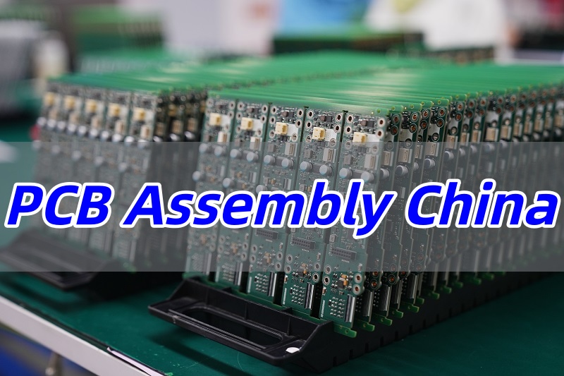
PCB Assembly China is the top choice for global electronics brands. This guide explains why China dominates the market and how EBest Circuit (Best Technology) delivers quality, speed, and cost efficiency for your projects.
Do you face these challenges in your electronics production?
High costs eating into your profit margins.
Long lead times delaying product launches.
Inconsistent quality causing rework and returns.
Poor communication with overseas suppliers.
Limited technical support for complex designs.
These pain points are challenging. But they can be solved by reliable China PCB assembly service suppliers.
Competitive pricing without sacrificing quality.
Reliable lead times with on-time delivery.
Strict quality control for consistent output.
English-speaking teams for smooth communication.
Expert engineering feedback to optimize your design.
At EBest Circuit (Best Technology), we specialize in high-end PCB assembly for global clients. Our advanced facility, certified processes, and customer-first approach make us a trusted partner. Contact us at sales@bestpcbs.com to start your project.
Why Choose PCB Assembly China for Your Electronic Projects?
In the global electronics landscape, choosing where to manufacture your printed circuit board assemblies (PCBA) is a critical decision. While many options exist, China has consistently remained the dominant hub. Why choose PCB assembly China for your electronic projects? The reasons extend far beyond low cost, encompassing a powerful trifecta of advanced technology, unparalleled supply chain efficiency, and proven manufacturing excellence.
Here’s a breakdown of the key advantages:
Unmatched Cost-Efficiency Without Compromise It’s no secret that competitive pricing is a major draw. However, the real advantage lies in the structure of the cost savings. China’s deeply rooted electronics ecosystem means:
Localized Supply Chain: Key components, raw materials like FR4 substrates, and machinery are often produced domestically. This drastically reduces logistics and import costs that other regions face.
Economies of Scale: High-volume production capabilities allow manufacturers to optimize operational costs, passing the savings on to you. This makes China ideal for both low-volume PCB assembly runs and mass production.
Advanced Technical Capabilities and Expertise China’s PCB industry has evolved from basic assembly to handling highly complex projects. Leading manufacturers like EBest Circuit (Best Technology) invest heavily in state-of-the-art equipment and skilled engineers. We specialize in:
Advanced techniques for flexible PCB assembly and aluminum PCB assembly for LEDs.
Sophisticated processes like surface mount technology (SMT) and through-hole assembly, supported by automated optical inspection (AOI) and X-Ray testing.
Robust and Resilient Supply Chain Speed to market is crucial. China’s integrated supply chain is a significant accelerator. From PCB fabrication and assembly to component sourcing and box-build, a true one-stop PCB assembly service under one roof minimizes delays. This turnkey approach simplifies your logistics, reduces management overhead, and ensures better control over the entire production timeline.
High Quality Standards and Stringent Certifications The outdated notion of variable quality is just that—outdated. Reputable PCB assembly companies in China adhere to international quality standards. At EBest Circuit (Best Technology), our operations are certified under ISO 9001, IATF 16949 (for automotive), ISO 13485 (for medical devices), and AS9100D (for aerospace). This rigorous framework guarantees that every board, from a PCB prototype assembly to a full production run, meets the highest levels of reliability and performance.
Proven Experience as a Global EMS Partner China has been the world’s workshop for decades. This means its top manufacturers have vast experience serving diverse international clients. This experience translates into:
Better understanding of global market requirements (CE, UL, RoHS compliance).
Skilled project management teams accustomed to bridging time zones and cultural differences.
Established logistics networks for reliable worldwide shipping.
EBest Circuit (Best Technology) differentiates ourselves through exceptional engineering support, transparent communication, and a commitment to building long-term partnerships. We transform the inherent strengths of PCB Assembly China into a tailored, low-risk, and high-value solution for your specific electronic projects. Pls feel free to contact our team today at sales@bestpcbs.com for a transparent PCB assembly China online quote.
Turnkey PCB Assembly China – EBest Circuit (Best Technology)
A turnkey solution simplifies everything. EBest Circuit (Best Technology) provides a full-service experience. We manage the entire process for you. This includes PCB fabrication, component sourcing, assembly, and testing. You get a finished product ready for use.
Design Review: Our engineers check your files for manufacturability. They suggest improvements to boost reliability and cut cost.
Material Procurement: We source components from trusted suppliers worldwide. Our buying power gets you the best prices.
PCB Fabrication: We make the boards in-house. This controls quality and speeds up the process.
Assembly (SMT & Through-Hole): We use automated lines for precise placement and soldering.
Testing and Inspection: Every board undergoes strict checks. We use AOI, X-Ray, and functional testing.
This approach saves you time and reduces risk. You have one point of contact. You get full traceability. Projects move faster and with fewer errors. For PCB prototype China projects, the same care applies. We build prototypes with production-level quality. This ensures a smooth transition to volume orders.
What Makes EBest Circuit (Best Technology) Stand Out Among Top 10 PCB Manufacturers in China?
The list of top 10 PCB manufacturers in China includes many big names. EBest Circuit (Best Technology) earns its place through technical excellence and customer service. We invest in the latest equipment. We maintain strict quality certifications. Our team solves complex manufacturing challenges daily.
Here’s what sets us apart:
Advanced Engineering Support: We help optimize designs for cost and performance.
High-Level Automation: Our SMT lines ensure accuracy and repeatability.
Rigorous Quality Systems: We follow ISO 9001, IATF 16949, ISO 13485, and AS9100D standards.
We serve many industries. These include medical, automotive, and aerospace. Each sector has unique requirements. Our team understands these needs. We deliver PCBs that meet strict reliability standards.
Technical Capability for PCB Assembly Manufacturer China
EBest Circuit (Best Technology) handles a broad range of projects. Our capabilities include:
We work with prototypes and high-volume orders. Our equipment includes high-speed SMT lines, automated optical inspection (AOI), and X-Ray systems. These tools ensure every board is built correctly.
For specialized needs like China LED PCB assembly or China medical PCB assembly, we have specific experience. We understand the thermal management needs of LED boards. We follow strict traceability for medical devices. For our clients, this means one less thing to worry about in a complex development cycle.
High-Quality Standards in PCB Manufacturing and Assembly China
Quality is non-negotiable in electronics. EBest Circuit (Best Technology) has built a robust quality system. It covers every step from incoming materials to final shipment.
Our quality process includes:
Incoming Component Verification: We check all parts for authenticity and condition.
In-Process Checks: Operators and machines inspect boards at each stage.
Final Functional Test: We validate that the assembled PCB works as intended.
We use advanced equipment like SPI (Solder Paste Inspection) and ICT (In-Circuit Test). This data-driven approach minimizes defects. It ensures that every product we ship meets your specifications.
What Certifications Should a Reliable China PCB Board Assembly Factory Have?
Certifications prove a factory’s commitment to quality. When choosing a partner, look for these key certifications:
ISO 9001: Quality Management System standard.
IATF 16949: Required for automotive manufacturing.
ISO 13485: Essential for medical device production.
AS9100D: The benchmark for aerospace quality.
EBest Circuit (Best Technology) holds all these certifications. They are not just certificates on the wall. They are part of our daily culture. Our team follows documented procedures. We undergo regular audits to maintain compliance.
How to Select Reliable PCB Assembly Companies in China?
Choosing the right partner is critical. Here is a simple checklist to guide your selection:
Technical Match: Can they build your specific type of board? Ask about similar projects.
Quality Certifications: Do they have relevant, up-to-date certifications?
Communication Skills: Is their team responsive and easy to understand?
Transparent Pricing: Do they provide clear, detailed quotes?
Supply Chain Stability: Do they have strong supplier relationships to avoid part shortages?
EBest Circuit (Best Technology) meets all these criteria. We encourage clients to audit our facility. We provide detailed quotes and design feedback. Our project managers speak fluent English. We make overseas collaboration simple and effective.
Case of China EMS PCB Assembly at EBest Circuit (Best Technology)
We serve a diverse client base. Here are two simplified examples:
Consumer Device Example: A client needed a compact, high-density board for a smart home device. We used micro-vias and fine-pitch BGAs. Our design team suggested changes to improve solderability. The result was a high-yield, reliable product launched on time.
Industrial Control Example: Another customer required a robust board for a factory controller. It needed wide temperature tolerance and high-voltage isolation. We selected appropriate materials and a conformal coating. The boards have performed perfectly in the field.
In conclusion, PCB Assembly China offers a powerful value proposition for global businesses. This article has outlined the key benefits and selection criteria. EBest Circuit (Best Technology) combines cost efficiency with high quality. We make the process simple and reliable. Our team is ready to support your next project. For a quick PCB assembly China online quote, please contact us at sales@bestpcbs.com.
FAQs
1. Which materials and boards require baking before assembly? To prevent moisture-related defects, the following items must be baked prior to assembly:
All Flexible Printed Circuit (FPC) boards.
Moisture-sensitive Integrated Circuits (ICs).
LED components.
2. What are the standard baking time and temperature parameters? Our standard baking profiles are as follows:
Conventional ICs: 120°C for 12 hours.
LEDs and Tape-and-Reel Components: 60°C for 12 hours.
FPCs and FR-4 Fiberglass Boards: 120°C for 1.5 hours.
3. What solder paste brands and alloys do you commonly use? We use high-quality solder pastes to ensure reliable connections:
For International Clients: Senju (Japan) – Alloy: Sn96.5%/Ag3.0%/Cu0.5% (SAC305).
Why docircuit board failure analysis? Let’s discover its benefits, common types, analysis process, troubleshooting and diagnosing techniques and case studies.
Identify the root cause and prevent recurrence: Using microscopic inspections (such as scanning electron microscopy and X-ray energy spectrum analysis) and electrical testing, we can accurately identify whether the fault point is a design defect, material degradation, or process error. For example, a car company recalled a batch of circuit boards due to poor soldering. After analysis, they improved soldering parameters and reduced the recurrence rate by 90%.
Improve product reliability and lifespan: Statistical analysis shows that the mean time between failures (MTBF) of industrial control boards that undergo failure analysis increases by approximately 30%. Accelerated life testing under environmental stresses such as high temperature and vibration can reveal potential failure modes in advance.
Reduce production costs and maintenance expenses: Early failure analysis can reduce after-sales repair costs. According to industry reports, in the consumer electronics sector, optimizing layouts by analyzing short circuits can reduce single-board repair costs by 45%, while also reducing spare parts inventory pressure.
Assist design iteration and technological innovation: Analyzing signal integrity issues in high-frequency circuits can provide data support for next-generation PCB routing rules. For example, by analyzing impedance mismatch cases in 5G base station circuit boards, the bit error rate has been optimized to below 10^-12.
Meeting Industry Compliance and Safety Standards: Sectors such as aerospace and medical devices require compliance with standards such as ISO-26262 and IEC-60601. Failure analysis reports are key evidence for certification, minimizing market access risks caused by compliance issues.
Shortening Product Development Cycles: Analyzing faults during the prototype testing phase can reduce design iterations. One drone manufacturer reduced its R&D cycle by 20% by analyzing power module overheating issues.
Strengthening Supply Chain Quality Control: Performing destructive physical analysis (DPA) on supplier components allows for traceability of material batches. For example, a chip package cracking case prompted a buyer to establish a supplier fault archive, resulting in a 60% reduction in incoming material defect rates.
Common Circuit Board Failures Types
Soldering Defects: Account for 1/3 of total failures. Common issues include cold solder, dry solder, solder joint fractures, and solder bridges. For instance, thermal stress on solder in high-temperature environments can cause joint cracking, while flux residue may trigger short circuits. Mitigation requires automated soldering equipment and stringent process control to minimize defects.
Component Damage: Represents 1/3 of total failures, primarily involving aluminum electrolytic capacitor degradation (1μF–330μF most prone to failure), resistor/optoisolator/ceramic capacitor damage, and high-voltage/high-current components like switching power supply rectifiers and VFD IGBT modules. Diagnose using multimeters, capacitance meters, or VI curve testers to identify parameter anomalies.
Circuit Faults: Comprise 1/3 of total failures, encompassing open/short circuits, copper trace fractures, and corrosion. Humid environments causing insulation damage account for 42% of short-circuit faults, while mechanical vibration may induce PCB cracking/bending. Fault localization combines visual inspection with electrical testing.
Design Flaws: Include improper layout causing thermal issues (e.g., chip overheating), power supply design defects leading to voltage instability, incorrect component selection (e.g., resistor tolerance mismatches), and signal crosstalk due to insufficient spacing. For example, a communication board experienced short-circuiting from incomplete etch traces, resolved via thermal design optimization and signal integrity analysis.
Environmental Factors: High temperature (>85°C accelerates component aging), high humidity (>70% causes condensation/short-circuits), corrosive dust (salt-laden particles degrade metal contacts), and ESD events dominate failure causes. Example: Southern China’s rainy season equipment failures due to humidity-induced shorts require dehumidifiers and dust covers.
Material Issues: Substandard PCB materials cause delamination/voids, improper copper foil weight induces heating, flux residue causes leakage, and chemical leaks (e.g., capacitor electrolyte corrosion). Rigorous raw material quality control and manufacturing parameter adherence are critical.
Software/Firmware Issues: Account for 1/3 of failures, including program loss, parameter errors, and software conflicts. PLC input signal anomalies often stem from loose sensor connections or EMI, resolved via program backups and robust EMI shielding design.
How to Perform Circuit Board Failure Analysis?
1. In-depth Failure Background Investigation and Standardized Data Acquisition
Establish diagnostic framework per IEEE 1445 standards, documenting failure phenomena (e.g., equipment non-startup, signal interruption), environmental parameters (temperature/humidity, voltage fluctuations), failure stages (design debugging/early failure), and historical data. IPC-9111 mandates cross-functional team collaboration (engineering, quality, operations) for deviation analysis and solution validation.
Case Example: Communication board short-circuit due to incomplete etching resolved by identifying moisture control failure during production, leading to etching process optimization.
2. System Electrical Performance and Structural Testing
Conduct system electrical tests using oscilloscopes, network analyzers, and multimeters. X-ray inspection (ASTM E1417-compliant) detects internal solder joint defects (e.g., BGA voids), while thermal imaging identifies abnormal hotspots (e.g., power transistor overheating). Electrical parameter tests cover static (resistance/capacitance) and dynamic (signal waveforms/noise) dimensions, with functional tests verifying signal stability (e.g., DisplayPort compliance).
Case Example: Audio board intermittent sound resolved by identifying abnormal solder joint resistance through electrical testing, followed by re-soldering.
3. Combined Non-Destructive and Destructive Analysis
Non-destructive methods: C-SAM ultrasonic microscopy for interlayer defect detection, SEM/EDS for material composition analysis (e.g., dendrite morphology), FTIR for flux residue verification.
Destructive methods: Microsectioning (IPC-TM-650 2.1.1) for internal structure observation, dye-and-pull (red ink) testing for BGA crack detection, solderability testing (J-STD-002) for coating quality assessment.
Case Example: Control board corrosion from capacitor leakage resolved via SEM/EDS identification of P/Ni-containing contaminants, leading to capacitor replacement and conformal coating optimization.
4. Root Cause Verification and Simulation Experiments
Develop fault tree models and replicate failure modes through accelerated aging (IEC 60068-2-14), salt spray corrosion (ASTM B117), and thermal simulation. Validate design flaws (e.g., impedance mismatch) or material issues (e.g., PCB delamination).
Case Example: Industrial board chip overheating resolved via thermal simulation optimizing heat dissipation channels, reducing chip temperature by 20%.
5. Repair and Reliability Enhancement Solutions
Soldering repair employs temperature-controlled soldering irons (320°C-380°C, ≤3 seconds heating) for rework or conductive silver paste filling. Component replacement adheres to IPC-A-610 standards, ensuring polarity (e.g., electrolyytic capacitors) and parameter matching.
Preventive measures: Hollow-core layer technology for signal integrity, MCP packaging for space savings and moisture resistance, solid-state circuit boards for vibration/EMI resistance.
Case Example: Motor drive board non-startup due to circuit break resolved by jumper wiring and reinforced insulation, followed by 24-hour full-load aging test.
6. International Standards
Adhere to IPC-9111, J-STD-001, and other international standards for standardized processes. For international clients, emphasize design reviews (DFM/DFA), process validation (solder paste printing optimization), and quality traceability (batch management).
Case Example: Cross-border team rapidly identified capacitor failure root cause through shared IPC/GJB standard comparison databases, optimizing supplier selection.
7. Preventive Maintenance
Implement regular cleaning (IPA + non-woven cloth), solder joint oxidation checks, and surge protection for power stability. Develop failure case libraries (root cause trees, solution repositories) with AI-assisted platforms reducing diagnostic cycles by 30%.
How to Choose Circuit Board Failure Analysis Tools?
1. Define Detection Requirements and Scenario Matching
Fault Type Localization: Select specialized tools based on common failure types (e.g., open/short circuits, component failure, soldering defects). Examples:
Basic Maintenance: Use digital multimeters (e.g., Fluke 87V, accuracy 0.05%+3) for voltage/current/resistance measurements; oscilloscopes (e.g., Rigol DS1054Z, 50MHz upgradable to 100MHz) to capture signal waveforms; bridge testers for capacitance/inductance analysis.
High-Speed Signal Analysis: Vector network analyzers (VNA, e.g., Keysight E5063A) for S-parameter measurement and impedance matching evaluation; Time-Domain Reflectometers (TDR) to locate transmission line breaks or impedance discontinuities.
Manufacturing Defect Detection: Automated Optical Inspection (AOI, e.g., Omron VT-S730) with high-resolution cameras for solder joint defects; flying probe testers supporting 0.1mm pitch test points without dedicated fixtures; X-ray inspection systems to analyze BGA solder ball voids or inner-layer trace defects.
2. Technical Parameters and Performance Adaptation
Accuracy and Resolution: Laboratory-grade scenarios require >0.1% accuracy (e.g., power quality analyzers), while general maintenance accepts 1%-3% accuracy. Digital instruments must consider resolution (e.g., 6.5-digit) and range coverage (e.g., >1000V for high-voltage applications).
Frequency and Bandwidth: High-frequency circuits (e.g., USB 3.0/PCIe) demand oscilloscopes with ≥100MHz bandwidth; signal integrity analysis requires VNAs supporting GHz-range frequencies.
Anti-Interference and Environmental Adaptability: Industrial environments require CAT III/IV safety certifications (IEC 61010) and IP54/IP67 protection for humid/dusty conditions; battery life focuses on durable lithium-ion solutions.
3. Tool Types and Functional Extensibility
Hardware Tools:
Specialized Detection Devices: Logic analyzers (e.g., Saleae Logic Pro 16) for multi-channel digital signal analysis; thermal imagers (e.g., FLIR T540, thermal sensitivity ≤0.03°C) for heat distribution visualization; BGA rework stations for precision soldering/desoldering.
Maintenance Auxiliary Tools: Hot air guns/constant-temperature soldering stations for SMD component handling; short-circuit trackers for rapid fault localization; signal generators to simulate input signals.
Software Tools:
PCB Design Software: Altium Designer (supports 3D real-time display and multi-layer board design), KiCad (open-source, ideal for beginners), EAGLE (compatible with Mac/Linux, rich community resources).
Simulation and Analysis Software: Integration with SPICE environments (e.g., Multisim) for circuit performance validation; data management tools supporting Gerber file generation and BOM integration.
Maintenance and Services: Prioritize brands offering local technical support, ≥1-year warranty, and periodic calibration services. Modular designs enable quick upgrades (e.g., oscilloscope bandwidth expansion), avoiding redundant investments.
Compatibility and Scalability: Tools must support standardized data interfaces (USB/LAN/GPIB) for seamless integration with existing production systems. Software tools should comply with mainstream operating systems and design standards (e.g., IPC, ISO).
5. Operational Convenience and Training Support
User-Friendly Interface: Tools should feature intuitive interfaces supporting automated testing, data analysis (e.g., machine learning for fault trend prediction), and report generation. For example, AOI systems use image algorithms to auto-compare against “perfect board” references.
Training and Documentation: Suppliers must provide operation manuals, video tutorials, and on-site training. Altium Designer, for instance, offers online courses and community support to accelerate designer onboarding.
Safety Compliance: Strict adherence to international safety standards (e.g., CE, UL certifications) ensures safe operation in high-voltage/industrial environments; ESD-safe tools (e.g., anti-static brushes, tweezers) minimize component damage.
Utilize 200× electron microscopy to scan solder joint surfaces, revealing nanoscale oxidation layers between solder and copper foil that cause “cold soldering” defects with elevated contact resistance. For instance, a power module with BGA cold soldering experienced intermittent power loss. After precise localization and repair via microscopy, failure rates dropped by 90%.
Power Rail Ripple Noise Quantification & Tolerance Standards
Oscilloscope measurements of +5V power rails must meet ≤50mV ripple noise limits per IPC-610 standards. Excessive ripple can trigger digital circuit errors. A communication base station motherboard saw a 85% reduction in signal transmission errors after replacing degraded 0.1μF/X7R filtering capacitors.
Thermal Simulation vs. Real-World Thermal Validation
ANSYS thermal simulation establishes 3D thermal models for PCBs, validated against thermal imaging data to verify heat dissipation paths. An industrial control board with aged thermal paste between heatsink and chip exhibited 3× higher thermal resistance, reaching 125°C (exceeding 105°C spec). After reapplying ≥5W/m·K thermal paste, temperatures dropped to 85°C.
High-Speed Signal Integrity 3D Analysis System
For ≥10Gbps signal lines, TDR detects impedance discontinuities (±10% tolerance), while eye diagram analysis measures rise time, jitter, and noise margins. A server motherboard with DDR4 bus impedance mismatch saw eye closure; adjusting PCB stack-up to 85-95Ω reduced bit error rates to 10⁻¹².
Build databases documenting typical failures like capacitor leakage, resistor burnout, and gate oxide breakdown. A power module with rising ESR (50mΩ→200mΩ) in aluminum electrolytic capacitors was quickly identified and replaced with low-ESR solid-state capacitors, extending lifespan 5×.
ICT Automation & Boundary Scan Synergy
ICT bed-of-nails testing achieves 30-second per-board inspection for opens/shorts and component value deviations. Combined with JTAG boundary scan, BGA chip logic can be in-system programmed (ISP) and diagnosed. A consumer electronics production line achieved 99.2% fault detection using ICT+boundary scan.
Spectrum analyzers scan PCB radiation noise to pinpoint 100MHz-1GHz sources from switching power supplies. Adding common-mode chokes, X/Y capacitors, and metal shields reduced noise 10dB below CISPR 22 Class B limits. A medical device motherboard passed FCC certification post-EMC retrofit.
Hardware-level logic analyzers capture bus signals (I?C/SPI), while software debuggers step through code to synchronize hardware signals with software expectations. An embedded system with incorrect SPI clock configuration was rapidly diagnosed and fixed via register adjustment.
Accelerated Aging Test & Reliability Growth Modeling
Post-repair boards undergo 168-hour 85°C/85%RH testing, with Arrhenius models predicting component lifetimes. An avionics board identified 10% latent failures via aging test, reducing failure rates to 0.1%/1000 hours per DO-160G standards.
Preventive FMEA Application for Failure Modes
FMEA identifies critical failure modes (e.g., solder fatigue, parameter drift) to implement targeted countermeasures. An automotive ECU added NTC thermistors to monitor overtemperature risks in power management chips, improving reliability 3×.
How to Diagnose a Faulty Circuit Board?
Step 1: Initial Visual Screening
Inspect the circuit board surface for obvious burn marks, component bulging/cracking (such as capacitor leakage, resistor carbonization), poor/broken solder joints, and corroded metal traces.
Pay special attention to corrosion on high-power components (such as power transistors and inductors), connector areas, and any signs of corrosion from use in humid environments. Surface-mount components should be inspected for any loosening or displacement.
Step 2: Environmental and Usage Condition Verification
Record the equipment’s operating environment (temperature, humidity, dust), power supply stability, and load conditions. High temperatures and high humidity can easily cause component oxidation and short circuits; frequent plugging and unplugging of connectors can cause poor connections; and overvoltage or undervoltage power supply can damage the power supply chip.
Step 3: Power System Test
Use a multimeter to measure input voltage at power terminals (e.g., DC 5V/12V/24V) against specifications. Investigate adapters, fuses, or power ICs if readings deviate. Test for shorts between power rails using resistance mode (near-zero ohms indicates shorts from capacitor failure or debris). Track voltage at critical nodes (e.g., chip power pins) during operation to detect opens or abnormal loads.
Step 4: Component Function Verification
Capacitors: Use a multimeter’s capacitance range/ESR meter to measure capacitance and equivalent series resistance. Bulging or leaking capacitors typically have decreased capacitance or increased ESR.
Resistors/Diodes: Measure resistors with power off to ensure they are within ±5% of their nominal values. Diodes must conduct forward (voltage drop 0.3-0.7V) and block reverse.
Semiconductors: Use the diode range to measure the conductivity between each electrode of transistors/field-effect transistors. Chips can be verified by replacing them or measuring the voltage at their power pins.
Special Components: Use an oscilloscope to measure crystal oscillator waveforms, relay contact contact, and optocoupler transmission to ensure positive signals.
Step 5: Signal Tracing and Waveform Analysis
For digital circuits, monitor clock signals (e.g., crystal outputs) and control lines (e.g., GPIOs) for stable waveforms using oscilloscopes. Use logic analyzers to capture bus signals (I²C/SPI/UART) and detect communication errors.
For analog circuits, inject reference signals (e.g., 1kHz sine wave) to trace signal loss points.
Step 6: Systematic Troubleshooting and Tool Application
Sectional Isolation Method: Divide the circuit board into power, control, and output modules, and power-off each section to narrow down the fault.
Comparison Method: Compare voltages, waveforms, or component parameters with a working board of the same model to quickly locate discrepancies.
Professional Tools: Use an infrared thermal imager to observe component temperature distribution (overheated areas may indicate a short circuit); an LCR meter to accurately measure inductance, capacitance, and resistance; and dedicated diagnostic software to simulate circuit behavior and identify design flaws or component aging.
Step 7: Repair Verification and Long-Term Maintenance
After replacing the damaged component, perform full functional testing (e.g., power-on test, load test, and long-term operation test) to confirm that the fault has been completely eliminated.
Repair procedures and test data should be recorded and compiled into a diagnostic report to facilitate subsequent maintenance or design optimization. For complex faults, analyze component failure modes (e.g., capacitor electrolyte drying, chip thermal aging) to prevent recurrence.
Circuit Board Failure Analysis Case Studies
Intermittent Power Loss Analysis and Resolution for Automotive ECU Circuit Boards
Problem Phenomena and Initial Diagnosis
Vehicles experienced sudden engine stalls during operation, with normal function briefly restored after restart. Diagnostic equipment detected no error codes, and external circuit checks revealed no anomalies.
Power voltage monitoring showed ECU supply voltage fluctuating between 9V-14V, significantly below the stable 12V requirement. Oscilloscope measurements revealed a 62mV ripple noise on the +5V power rail, exceeding the IPC-610 standard limit of ≤50mV, indicating power irregularities as the primary trigger.
Advanced Failure Localization and Technical Analysis
Microscopic Solder Joint Inspection: 200× electron microscopy identified nanoscale oxidation layers on BGA solder joints, causing “cold soldering” defects with elevated contact resistance. Such latent defects are invisible to the naked eye but lead to intermittent power interruptions.
Thermal Simulation and Validation: ANSYS thermal modeling confirmed 3D heat distribution, revealing aged thermal paste between heatsink and chip (thermal conductivity dropped to 1.2W/m·K), causing chip junction temperatures to reach 125°C (exceeding the 105°C specification). This accelerated solder joint oxidation due to thermal stress.
High-Speed Signal Integrity Analysis: TDR testing detected ±15% impedance deviations on DDR4 memory bus lines (standard tolerance ±10%). Eye diagram analysis confirmed signal rise time delays and insufficient noise margins, leading to system misinterpretation of data.
EMC Noise Source Identification: Spectrum analysis pinpointed 100MHz-1GHz radiation noise from the switching power module. Adding common-mode chokes and X/Y capacitors reduced noise by 10dB below CISPR 22 Class B limits.
Solution Implementation and Validation
Solder Joint Repair and Component Upgrade: Reflowed cold solder joints and replaced high-ESR electrolytic capacitors with low-ESR solid-state capacitors (ESR reduced from 200mΩ to 50mΩ), bringing power ripple down to 38mV and meeting IPC-610 standards.
Thermal Management Optimization: Applied high-thermal-conductivity paste (≥5W/m·K) and optimized heatsink contact area, stabilizing chip temperatures below 85°C. Passed 168-hour 85°C/85%RH aging tests with no recurrence.
Impedance Matching Adjustment: Optimized PCB stack-up to maintain 85-95Ω impedance on high-speed lines, improving eye diagram opening by 40% and reducing bit error rates to 10???.
FMEA-Based Preventive Measures: Integrated solder fatigue and component drift into a failure mode database. Implemented NTC thermistor-based temperature monitoring and dynamic frequency scaling, enhancing reliability by three orders of magnitude.
PCB manufacturers South Africa form a vital part of the nation’s expanding electronics sector. This article provides a clear comparison between local suppliers and international partners to help you make the best sourcing decision.
But what if your local supply chain can’t keep up? You’re likely to face these common frustrations:
Facing longer lead times than initially promised.
Encountering technical limits with complex designs.
Struggling with higher costs for materials and production.
Dealing with inconsistent quality control on orders.
Experiencing limited options for advanced PCB technologies.
The right global partner solves these issues by providing:
Faster and more reliable production turnarounds.
Expert support for even the most complex design requirements.
More competitive pricing due to scaled manufacturing.
Rigorous quality certifications and consistent output.
Access to advanced capabilities like HDI and specialized substrates.
We are EBest Circuit (Best Technology), a specialized PCB manufacturer from China with proven expertise in demanding applications. We reliably produce boards from 1 to 32 layers, with extreme copper weights up to 30oz for high power and ultra-thin boards down to 0.15mm. Our capabilities include advanced technologies like impedance control and blind/buried vias, backed by our own SMT factory for full turnkey solutions. We focus on delivering measurable quality and reliability for clients in South Africa and beyond. Pls feel free to contact us at sales@bestpcbs.com to discuss your project needs.
Why PCB Manufacturers South Africa Are in High Demand?
The growing consumer market for electronics and supportive industrial policies are fueling significant demand for Printed Circuit Boards (PCBs) in South Africa. While local PCB manufacturers South Africa are essential to the ecosystem, this surge is testing the limits of domestic capacity, revealing clear opportunities for international partnerships to ensure a resilient supply chain.
Expanding End-Market Consumption The rising adoption of smartphones, IoT devices, and renewable energy solutions (e.g., solar inverters) in South Africa directly increases the need for high-quality PCBs. Rapid product lifecycles require responsive prototyping and reliable volume production, placing pressure on the entire supply chain.
Support for Local Manufacturing and Assembly Government initiatives aimed at “re-industrialization” encourage local assembly and manufacturing. Companies in the automotive, industrial automation, and telecommunications sectors consequently require stable, dependable PCB suppliers to support their production schedules and growth ambitions.
The Dual Reality of Local Supply
Strength: Proximity allows for better communication, faster prototype turnaround, and closer collaboration during the initial product development stages.
Limitation: The local PCB industry is largely composed of small to medium-sized enterprises. When faced with orders for high-volume, high-layer-count (e.g., >20 layers), or advanced technology (e.g., heavy copper >6 oz, HDI) boards, they often encounter capacity and technical ceilings.
In summary, the demand for PCBs in South Africa is robust and driven by solid market forces. However, the existing local supply chain faces challenges in meeting the needs for advanced, high-volume production. This situation not only underscores the critical role of local PCB board manufacturers South Africa but also makes a compelling case for forming strategic partnerships with international PCB suppliers like EBest Circuit (Best Technology). Such collaboration is a pragmatic strategy for South African businesses to secure their supply chain, access advanced capabilities, and enhance their global competitiveness.
What Challenges Do PCB Manufacturing Companies in South Africa Face?
The local industry has unique strengths. But it also faces real-world hurdles. Understanding these challenges is key to finding the right solution.
First, delivery timelines can be a concern. Local factories may have limited production slots. This can extend lead times, especially for larger orders.
Second, technical complexity presents a barrier. Not all local PCB manufacturing companies are equipped for highly advanced boards. Think of boards with 16 layers or more. Or designs for high-frequency or high-power applications.
Finally, cost control remains difficult. Raw material imports affect final pricing. This can impact your project’s budget.
For specialized needs, South African companies often look abroad. Partners like EBest Circuit (Best Technology) fill this gap. We deliver complex solutions—from high-layer-count boards to robust metal-core designs. This ensures your most ambitious projects become reality.
Comparing PCB Manufacturing Johannesburg, Pretoria, and Cape Town
South Africa’s industrial landscape is diverse. The major hubs each have distinct characteristics. Let’s explore the scenes in three key cities.
PCB Manufacturing Johannesburg As the economic heartland, Johannesburg hosts several industrial players.
Trax PCB: A well-known name offering a range of PCB services, focusing on prototype and small-batch production.
ASM Industries: Provides assembly and manufacturing services, serving various industrial sectors in the Gauteng region.
Circuitec: Specializes in quick-turn PCB prototypes, catering to the fast-paced development needs of local engineers.
PCB Manufacturing Pretoria The administrative capital has a growing tech manufacturing base.
Polar PCB: Known for its reliability in double-sided and multilayer PCB production for the local market.
Proton Electronics: Offers both PCB fabrication and component assembly services.
Elvey Group: A major distributor and manufacturer serving the security and telecom industries with relevant PCB solutions.
PCB Manufacturing Cape Town The coastal hub is a center for innovation and green technology.
Skywire Technologies: Works closely with the renewable energy and IoT sectors, providing tailored PCB solutions.
Cape Electronics: A long-standing manufacturer serving the industrial and consumer electronics markets.
Tekmatron: Focuses on control systems and offers in-house PCB manufacturing for its products.
Despite these local options, many South African businesses choose to collaborate with Asian manufacturers. This strategy offers a compelling advantage. It combines higher cost-effectiveness with mature, high-volume production capabilities. This is a smart way to access world-class quality.
Why Many Printed Circuit Board Companies in South Africa Source from China?
South African electronics companies are increasingly looking to China for their PCB needs, a trend driven by a strategic need to overcome local supply chain limitations and enhance global competitiveness. This shift is not just about cost; it’s about accessing a level of capability, scale, and reliability that is difficult to find elsewhere.
The decision to partner with Chinese manufacturers is typically based on a few critical factors where local sourcing often faces challenges. Here is a breakdown of these key advantages, illustrated with concrete examples from a manufacturer like EBest Circuit (Best Technology) to show what is possible.
1. Access to Advanced and Specialized Manufacturing Capabilities
Many local PCB providers excel at standard designs but hit a technical ceiling with more complex requirements. Chinese manufacturers have built their expertise on serving a global market that demands cutting-edge technology.
It means your product designs are not limited by what your local supply chain can produce. You can innovate with confidence.
For instance, a manufacturer like EBest Circuit (Best Technology) can reliably produce boards with extreme specifications, such as 30-ounce copper for high-power applications (common in solar inverters or industrial drives) or ultra-thin 0.15mm boards for miniaturized devices. They also routinely handle high-layer counts (e.g., 20+ layers) and advanced HDI processes. This level of capability ensures that even your most technically demanding projects are feasible.
2. Unbeatable Combination of Scale, Speed, and Cost
China’s mature electronics ecosystem creates significant efficiencies that individual regional hubs struggle to match. This translates into direct benefits for your business’s bottom line and agility.
You can achieve lower per-unit costs on volume production without sacrificing quality, and get your products to market faster.
The integrated supply chain allows for competitive material pricing and rapid turnaround. For a full turnkey service (where the manufacturer also handles component sourcing and assembly), a proficient Chinese partner can often complete SMT assembly in 2-3 days post-material confirmation. This speed and cost-effectiveness are crucial for staying competitive.
3. Supply Chain Reliability and Proactive Partnership
Beyond just making boards, leading Chinese manufacturers act as strategic partners, offering transparency and support that mitigates risk.
You gain a predictable and reliable supply chain partner, reducing production delays and ensuring consistent quality across orders.
Reliable partners implement rigorous quality control following IPC-A-600 Class 2/3 standards, provide full production tracking (WIP), and offer engineering support like Design for Manufacturability (DFM) analysis. Furthermore, reputable manufacturers strictly respect their clients’ business, ensuring they never bypass you to contact your end-customers, which is a critical assurance for South African traders and designers.
In closing, South African companies source from China to solve specific business and technical challenges. The primary reasons are access to advanced technologies that enable product innovation, the economic advantages of scale and efficiency, and the operational security of a highly reliable supply chain.
Partnering with a qualified Chinese manufacturer is not about replacing local suppliers but about building a complementary, strategic relationship that elevates your capabilities and allows you to compete effectively on a global stage.
How to Find the Best PCB Manufacturers South Africa Can Rely On?
Selecting a PCB manufacturer is a strategic decision that impacts product quality, supply chain stability, and long-term success. For companies in South Africa, where logistics and technical support can be challenging, a rigorous evaluation based on concrete data is essential. Here is a structured framework for your selection process.
1. Scrutinize Certifications and Quality Control Systems
Certifications are not just paperwork; they are evidence of a systematic approach to quality. A reliable manufacturer must have internationally recognized certifications.
Key Certifications to Demand:
ISO 9001: The baseline for quality management systems.
IATF 16949: Non-negotiable for automotive electronics, ensuring process control and traceability.
ISO 13485: Essential for medical devices, focusing on risk management and documentation.
AS9100D: The aerospace standard, indicating the highest level of quality and reliability.
Beyond Certificates – Look for Process Evidence: A top manufacturer like EBest Circuit (Best Technology) employs a Manufacturing Execution System (MES) that tracks every board through production. Quality isn’t just inspected at the end; it’s built into every step. Their documentation shows adherence to IPC-A-600 Class 2/3 standards, with Class 3 (for high-reliability applications) typically costing 10-15% more but offering superior longevity and performance.
2. Evaluate Technical Capabilities Against Your Project Requirements
Technical specifications separate capable manufacturers from exceptional ones. Request a detailed Process Capability Matrix and verify it with data.
Parameter
Standard Capability
Advanced Capability
Significance for South Africa
Max Layers
32 layers
Up to 100 layers (with review)
Ensures support for complex designs in telecom or industrial tech.
Board Thickness
0.4 mm – 6.0 mm
0.15 mm – 10.0 mm
Flexibility for both lightweight consumer products and robust industrial equipment.
Inner Layer Copper
Up to 6 oz
Up to 20 oz
Critical for high-power applications common in power infrastructure and mining.
Outer Layer Copper
Up to 10 oz
Up to 28 oz
Allows for heavy-current carrying capacity.
Min. Laser Drill Via
0.10 mm
0.07 mm
Essential for HDI designs in advanced electronics.
Specialized Material Expertise
South Africa’s growing sectors, such as telecommunications and renewable energy, require specialized PCB materials. A reliable manufacturing partner should have proven experience with:
Thermal Management Solutions Example: Aluminum substrates with thermal conductivity up to 12 W/m·K – essential for LED lighting and power converters, capable of withstanding variable climates.
High-Frequency Materials Example: Rogers RO4350B (Dk = 3.48, Df = 0.0037) – ideal for 5G, radar, and high-speed telecom applications.
High-Speed Materials Example: Panasonic R-5775 (Df ≤ 0.004) – suitable for data centers and network hardware, ensuring signal integrity.
3. Assess Manufacturing Process Controls and Fault Prevention
The devil is in the details. A manufacturer’s ability to control intricate processes directly impacts yield and reliability.
Critical Process Controls
Contamination Control: Use of Ion Contamination Testers to ensure board cleanliness, which is crucial for long-term reliability in humid environments.
Impedance Control: Tolerances should be tight (±5Ω for <50Ω, ±10% for ≥50Ω). This is vital for signal integrity in high-speed designs.
Copper Plating: Hole wall copper thickness should be a minimum of 25 µm (1 mil), verified by cross-sectioning.
Solder mask Registration: Alignment tolerance of ±0.076 mm, preventing solder bridges.
Advanced Techniques: For complex designs, look for experience with embedded copper technology for thermal management or HDI (High-Density Interconnect) processes with stacked microvias. EBest Circuit (Best Technology)’s documentation outlines processes for 1+N+1 and 2+N+2 board structures, which are benchmarks for advanced manufacturing.
4. Analyze Communication, Transparency, and Logistics
A perfect board is useless if it doesn’t arrive on time or with opaque communication. This is especially critical for cross-continental partnerships.
Key Indicators of a Reliable Partner:
Detailed Work-in-Progress (WIP) Tracking: You should have visibility into every stage of production.
Responsive Engineering Support: They should proactively discuss Design for Manufacturability (DFM) issues, such as ensuring a 0.5mm minimum distance between a copper block edge and a drill hole to prevent delamination.
Packaging for Long-Distance Shipping: They must use vacuum sealing with desiccants to protect boards from moisture and salt air during sea freight to South African ports.
Clear Testing Options: Offering both flying probe testing for prototypes and dedicated test fixtures for mass production, with clear cost implications.
To find the best PCB manufacturer South Africa can rely on, move beyond marketing claims. Use this data-driven checklist:
Request Certifications: Confirm ISO 9001, IATF 16949, etc.
Review the Capability Matrix: Match their technical limits (layer count, copper weight, etc.) to your product roadmap.
Ask for a DFM Report: Submit a test Gerber file and have them generate a Design for Manufacturability report. This demonstrates their technical depth.
Inquire about Material Sourcing: Ensure they use reputable substrate suppliers (e.g., Shengyi, KB, ITEQ) to avoid quality fluctuations.
Clarify Logistics and Communication: Confirm WIP update frequency and packaging standards.
By following this structured approach, you can identify a partner like EBest Circuit (Best Technology)—one that provides not just boards, but a reliable, long-term extension of your engineering and supply chain capabilities.
Why EBest Circuit (Best Technology) Is the Trusted PCB Partner for South Africa?
For South African industries demanding reliability and performance, EBest Circuit (Best Technology) delivers unparalleled engineering expertise and quality assurance.
Proven Quality & Certifications
We meet the highest international standards, ensuring your products excel in any environment.
Global Certifications: ISO 9001, IATF 16949 (Automotive), ISO 13485 (Medical), AS9100D (Aerospace).
Rigorous Testing: 100% electrical testing, impedance control (±10%), and thermal shock resistance (288°C, 5 cycles).
Full Traceability: Our MES system tracks every board from material to shipment.
Advanced Technical Capabilities
We manufacture the complex, high-performance boards that power modern technology.
Heavy Copper & Power Electronics: Up to 30 oz copper for high-current applications in energy and mining.
HDI & Microvia Technology: Enabling smaller, faster, and more reliable devices for telecom and advanced electronics. We expertly manage complex blind and buried via structures to ensure signal integrity in sophisticated, space-constrained designs.
High-Frequency/Speed Expertise: Specialized materials (e.g., Rogers, Taconic) for critical 5G and communication infrastructure with superior signal integrity.
Engineering Partnership & Support
We act as an extension of your team, providing expert guidance to optimize your designs.
DFM Analysis: We proactively identify and resolve potential manufacturing issues before production.
Material Selection: We help you choose the ideal materials to balance performance, durability, and cost.
Value Engineering: Practical advice to enhance reliability, such as recommending ENIG surface finish over HASL for thick copper boards to prevent thermal stress.
Reliable Supply Chain & Transparency
We ensure a seamless, trustworthy partnership, regardless of distance.
Dedicated Project Management: Clear communication with regular Work In Progress (WIP) updates.
Logistics Optimized for Africa: Secure, vacuum-sealed packaging with desiccant to protect against humidity during transit.
Rapid Prototyping: Accelerate your time-to-market with our quick-turn prototyping services.
All things considered, EBest Circuit (Best Technology) combines certified quality, advanced engineering, and unwavering reliability to be the trusted PCB partner South African companies can depend on for long-term success.
Case of PCB Manufacturing South Africa Project at EBest Circuit (Best Technology)
EBest Circuit (Best Technology) has successfully partnered with multiple clients in South Africa across diverse industries, providing high-quality PCB solutions tailored to specific application requirements. Below are two detailed case studies showcasing our capabilities in handling complex projects with precise technical specifications.
Case 1: 8-Layer FR4 PCB for Surveillance & Security Equipment
Application Scenario: Surveillance & Security This PCB was designed for a high-performance security control system used in commercial and residential monitoring. The board supports high-speed data processing and stable signal transmission, ensuring reliability in 24/7 operation.
Technical Parameters:
Layer Count: 8 layers
Material: FR4, Tg 170
Surface Finish: ENIG 1U” (Immersion Gold)
Solder Mask: Blue with white silkscreen
Copper Thickness:
Inner Layers: 1 oz
Outer Layers: 1 oz
Final Thickness: 1.3 mm ±10%
Delivery Format: Panelized
Key Features:
High Tg material for thermal stability.
ENIG finish for excellent solderability and corrosion resistance.
Ideal for dense layouts and signal integrity in security hardware.
Case 2: 4-Layer Heavy Copper PCB for Automotive Control Systems
Application Scenario: Automotive Electronics This PCB was developed for an automotive engine control unit (ECU), requiring robust performance under high temperatures and vibrations. The heavy copper design ensures current-carrying capacity and durability.
Technical Parameters:
Layer Count: 4 layers
Material: High Tg 180
Surface Finish: ENIG 2U”
Solder Mask: Green with white silkscreen
Copper Thickness:
Inner Layers: 4 oz
Outer Layers: 4 oz
Dielectric Thickness: Uniform PP thickness per layer
Final Thickness: 1.40 mm ±10%
Testing: 100% Electrical Test (Flying Probe)
Key Features:
4 oz copper for high-power traction and thermal management.
High Tg material for resistance to automotive thermal cycles.
100% electrical testing guarantees zero defects.
In essence, south African clients trust EBest Circuit (Best Technology) for our industry-specific expertise, precision manufacturing, and fast turnaround. We deliver tailored solutions for automotive, security, and solar sectors, with tight tolerances (±10% thickness) and 100% electrical testing ensuring reliability. Our efficient production and panelized delivery meet tight deadlines. Pls contact us at sales@bestpcbs.com for your custom PCB needs.
In conclusion, PCB manufacturers South Africa are essential for local innovation. This guide has explored how global partnerships can complement local efforts to ensure a robust supply chain.
Navigating the landscape of PCB board manufacturers South Africa requires a strategic view. Balancing local support with international capability is often the wisest path. For those seeking a partner with proven expertise and a commitment to quality, EBest Circuit (Best Technology) stands ready. Our advanced manufacturing and dedicated service provide a reliable foundation for your products. Contact our team at sales@bestpcbs.com to start a conversation about your specific needs.
FAQs
1. What is the maximum temperature a PCB can withstand?
Standard PCB materials typically have an operating temperature range of 105-130°C. For higher temperature requirements of 150-170°C, specialized materials like Shengyi’s S7136 can be used, though these are generally limited to double-layer boards and may have minimum order quantity (MOQ) requirements.
2. Why are process margins required in PCB manufacturing?
Process margins (typically 5-8mm wide) are essential blank borders left on PCBs to accommodate SMT assembly equipment handling and to provide space for panelization markers used in automated manufacturing processes.
3. Why are BGA vias filled?
Vias in BGA areas (typically 0.2-0.35mm diameter) require filling to prevent solder paste or plating chemicals from accumulating in the holes during subsequent processing like HASL or ENIG. Unfilled or inadequately filled vias can trap contaminants or solder balls that may cause short circuits or component failure during high-temperature reflow soldering.
For specific technical requirements or any PCB specifications, please contact our engineering team at sales@bestpcbs.com for customized solutions.
How to cleancorroded circuit board? Let’s discover cleaning methods, repair methods and precautions, prevention methods for corroded circuit board.
Are you troubled with these problems?
Why does my circuit board easily corrode in humid environments, leading to frequent failures?
How can I enhance PCB durability and consistency without increasing costs?
During design iterations, how can I quickly obtain reliable samples to avoid project delays?
As a circuit board manufacturer, EBest Circuit (Best Technology) can provide you service and solution:
Advanced Anti-Corrosion Coating: We apply eco-friendly protective coatings specifically engineered for high-humidity environments, ensuring long-term circuit board stability and reducing failure risks.
Flexible Custom Production: Based on your design requirements, we provide rapid prototyping and volume production services, optimizing material selection to achieve high performance within budget constraints.
Efficient Supply Chain Support: Through streamlined logistics and real-time progress tracking, we guarantee fast response from design to delivery, allowing you to focus on innovation with peace of mind.
Welcome to contact us if you have any request for circuit board: sales@bestpcbs.com.
Moisture and Condensation: Atmospheric moisture condenses on circuit board surfaces, forming electrolyte films that accelerate electrochemical corrosion of metal traces. In high-humidity environments, capillary action in plating gaps and solder joint edges accumulates moisture even without direct submersion, amplifying corrosion risks.
Salt Spray Environment: Chloride ions in coastal or industrial zones degrade metal passivation layers, triggering pitting and intergranular corrosion. For example, silver plating in sulfide environments generates non-conductive silver sulfide, increasing contact resistance and impairing signal integrity.
Thermal Cycling Dew Formation: Frequent temperature fluctuations in equipment cause condensation on internal components, particularly pronounced in regions with significant diurnal temperature swings, accelerating corrosion through moisture accumulation.
Corrosion from Chemical Contamination
Flux Residues: Incompletely removed organic acid fluxes decompose into acidic compounds, with residues beneath components progressively corroding copper traces, leading to eventual circuit failure.
Industrial Gas Erosion: Acidic gases like sulfur dioxide and nitrogen oxides dissolve in water films to form acidic electrolytes, causing green patina (basic copper carbonate) on copper traces and tarnishing solder surfaces, reducing conductivity.
Biological Degradation: Organic acids from mold metabolism in humid environments erode epoxy substrates, while insect excreta introduce electrolytes that induce localized short circuits and corrosion.
Material and Process Defects
Dissimilar Metal Contact: Direct contact between metals with large electrochemical potential differences (e.g., copper and gold) in the presence of electrolytes forms galvanic cells, preferentially corroding the more active metal and shortening circuit lifespan.
Protective Coating Failure: Uneven, porous, or insufficiently thick conformal coatings allow corrosive agents to penetrate to metal surfaces, with microcracks exacerbated by vibration environments.
Electromigration: Prolonged electrical current drives directional movement of metal ions, forming whiskers or voids in conductors, accelerating conductor fracture and compromising circuit reliability.
Toolbox Configuration: Equip ESD gloves, safety goggles, and N95 masks. Use an ESD-safe work mat (surface resistance 10?–10? Ω) and a leakage-protected isolation transformer to maintain zero-potential workbench.
Component Tagging System: Apply a three-color labeling strategy during disassembly—red for high-risk components (e.g., crystals), yellow for components requiring retesting, and green for reusable parts.
Environmental Control: Maintain 40–60% humidity and use an ionizing blower to neutralize static. For lithium-battery-equipped boards, perform short-circuit tests (e.g., measure battery terminal impedance >1MΩ).
2. Advanced Mild Corrosion Treatment
Cleaning Agent Selection:
Alcohol-Based: 99.5% absolute ethanol (conductivity <1μs/cm) for flux residue; isopropanol (IPA) for precision solder joints due to faster evaporation.
Acidic Solutions: Citric acid solution (pH 3–4) for neutralizing alkaline corrosion on tarnished copper traces (avoid on aluminum components).
Three-Step Brushing Protocol:
Coarse brush for bulk corrosion removal.
Soft brush for fine cleaning.
Microfiber cloth with deionized water for residue-free final rinse.
3. Professional Stubborn Corrosion Removal
Chemical Soaking Parameters: Optimize 5–8% dilute phosphoric acid solution (volume ratio) with 5–15 minutes immersion. Pair with 40kHz ultrasonic cleaning at 0.3W/cm? for effective micro-pore debris removal.
Mechanical Polishing Standards: Use ≥2000-grit wet sandpaper, polishing parallel to circuit traces to avoid cross-hatching. Post-polish microscopic inspection ensures copper thickness retention >80% original.
4. Advanced Deep Corrosion Repair
Wire Bonding Protocol: Use 0.3mm silver-plated wire with 280°C hot air gun for conical, smooth solder joints. For high-frequency circuits, adopt coaxial wiring to minimize signal interference.
Substrate Upgrade Recommendations: In humid environments (RH>60%), use PTFE substrate with ENIG finish (5x corrosion resistance vs. HASL). For RF circuits, Rogers 4350B substrate (ε=3.48) ensures stable dielectric properties.
5. Systematic Drying & Protection
Vacuum Drying Process: Employ molecular sieve vacuum oven at -0.1MPa, 60°C for 4 hours to eliminate internal moisture. For plastic components, cap temperature at 85°C to prevent deformation.
Conformal Coating Application: Apply acrylic coating (e.g., Humiseal 1A33) at 50–70μm thickness. Use peelable coatings for repairable areas.
6. Standardized Testing & Maintenance
Enhanced Aging Test: Conduct 1000-hour accelerated aging at 85°C/85% RH, monitoring insulation resistance (>100MΩ) and conduction resistance drift (<5%). Use thermal imaging for hotspot detection.
Maintenance Cycle Optimization: Industrial equipment: 500-hour intervals; consumer electronics: quarterly. Halve intervals in harsh environments (e.g., high dust/humidity).
7. Ultimate Environmental & Safety Measures
Waste Treatment System: Recover heavy metals (e.g., Cu??) via ion-exchange resins (95% recovery). Dispose of non-recyclable waste per Hazardous Waste Regulations through certified agencies.
Emergency Response: For chemical exposure, flush skin with water for 15 minutes and apply neutralizers (e.g., boric acid). For inhalation, relocate to ventilated areas and administer oxygen; seek medical attention if severe.
Before cleaning, disconnect power and remove batteries to prevent short circuits or electric shock. Store sensitive components (e.g., ICs, capacitors) separately to avoid corrosion by cleaning agents. Control storage humidity below 30% RH and temperature at 20–25°C to slow corrosion rates, as per experimental data.
2. Mild Corrosion Treatment
Use a soft-bristled toothbrush dipped in anhydrous alcohol to gently scrub surface oxidation. Tests show that polishing copper foil edges with 2000-grit sandpaper and applying anti-oxidation agents restores over 90% of copper brightness. Ideal for mild corrosion like copper discoloration or peeling.
3. Stubborn Corrosion Removal
Soak in 5–10% phosphoric acid solution for 10 minutes, then use ultrasonic cleaner for 15 minutes to remove 95%+ of solder joint corrosion without damaging components. For green patina or stuck pins, heat solder to 350°C and use solder wick to remove old solder before re-tinning.
4. Drying & Functional Testing
Dry thoroughly with nitrogen gun or 80°C oven for 2 hours. Post-repair, verify continuity with a multimeter and monitor local potential differences via SKPFM electrochemical testing to ensure no hidden corrosion. Accelerated aging tests (85°C/85% RH for 1000 hours) predict remaining lifespan.
5. Protective Reinforcement
Spray acrylic conformal coating on repaired areas to block moisture/dust. Antioxidant paste on solder joints extends lifespan by 3x. PTFE substrates improve moisture resistance by 50% in humid environments. Electroless copper plating deposits 0.02mm copper layers to restore 98% conductivity to broken traces.
6. Tools & Materials Recommendations
Use pH 6.5–7.5 neutral detergents, anti-static brushes, lint-free cloths, and specialized electronic cleaners. Ultrasonic cleaners require deionized water to avoid strong acid/base damage. Clean industrial equipment monthly and consumer electronics quarterly; replace electrolyytic capacitors when capacitance drops below 80% of rated value.
7. Safety & Emergency Handling
Wear dust masks, chemical goggles, and rubber gloves. In case of acid leaks, rinse with water and neutralize waste. Flush skin with water for 15+ minutes and seek medical attention. For sudden corrosion (e.g., white salt deposits), rinse with deionized water and apply protective agents within 5 minutes.
8. Special Scenario Solutions
Copper edge oxidation: Polish with 2000-grit sandpaper + anti-oxidation coating.
Solder corrosion: Heat to 350°C + solder wick.
Large trace breaks: Electroless copper plating (0.02mm) + jumper wires.
Batch cleaning: Water-based spray systems compatible with water/chemical cleaning.
9. Maintenance & Lifespan Monitoring
Regularly monitor corrosion via 85°C/85% RH accelerated aging tests and SKPFM potential scans. Quarterly/monthly cleaning schedules improve lifespan prediction accuracy by 40%. Industrial/consumer devices benefit from structured maintenance cycles to maximize longevity.
How to Fix Corroded Circuit Board?
1. Power Disconnection and Safety Enhancement
Disconnect the circuit board from all power sources and confirm zero residual voltage using a multimeter.
Wear ESD-safe wrist straps and insulated gloves to prevent electrostatic discharge or accidental electric shock.
Use an anti-static mat for the workbench and opt for insulated tools (e.g., ceramic-tipped screwdrivers) to avoid short-circuiting components.
2. Deep Cleaning and Contaminant Removal
Use a soft-bristled brush with isopropyl alcohol (99% purity) or anhydrous ethanol for initial cleaning, focusing on removing flux residue and dust around solder joints and component leads.
For stubborn stains, gently wipe with a cotton swab lightly dipped in a specialized circuit board cleaner (such as Flux Remover), taking care to prevent liquid from seeping into the components. After cleaning, blow dry thoroughly with compressed air to ensure no liquid remains.
3. Precise Corrosion Identification
Inspect copper traces under a magnifier or microscope: healthy traces appear bright red, while corroded areas show green oxidation or black spots.
Check solder joints for cracks, voids, or lifted pads, and measure continuity with a multimeter’s diode test to locate breaks.
4. Graded Corrosion Treatment
Mild Corrosion: Dab 5% acetic acid (white vinegar) or lemon juice with a cotton swab to neutralize alkaline residues, then wipe clean with alcohol.
Moderate Corrosion: Gently polish oxidized layers with 600-800 grit sandpaper or a fiberglass pen until metallic shine returns to avoid scratching adjacent traces.
Severe Corrosion: For fully severed traces, clear endpoints with a micro-drill and re-solder with low-temperature solder (e.g., Kester 44 Rosin Core) or use conductive silver paint for repairs.
5. Refined Soldering and Component Care
Use a temperature-controlled soldering iron (250-300°C) with lead-free solder wire. Pre-tin pads and leads before soldering to ensure smooth, conical joints.
For SMD components, employ a hot air gun at low flow (30-40 L/min) to prevent thermal damage. Post-soldering, inspect joints for cold solder or voids under magnification.
6. Protective Coating Application
Apply conformal coating (e.g., MG Chemicals 838) using a spray system:
First Coat: Thin layer to penetrate crevices.
Second Coat: Moderate thickness for full coverage.
Third Coat: Thick layer for robust protection.
Maintain 20-30cm distance during spraying to avoid bubbles. Cure for 24 hours at room temperature.
7. Comprehensive Testing and Reliability Validation
Verify electrical parameters (voltage, resistance) with a multimeter and conduct functional testing under simulated operating conditions.
Perform accelerated life testing: 48 hours at 60°C/90% RH to detect latent failures. For critical applications, add vibration (10-55 Hz, 1.5mm amplitude) and shock testing (15g, 11ms) to ensure durability.
Corroded Circuit Board Repair Precautions
1. Ensure Power Is Completely Disconnected Before Operation
Unplug the power source and remove the battery. Use a multimeter to confirm no voltage remains. For repairs in humid environments, preheat the workbench with an electric blanket for 30 minutes to eliminate moisture and prevent secondary corrosion.
2. Equip Full Protective Gear
Always wear an anti-static wrist strap (grounded), rubber gloves, safety goggles, and an N95 mask. If corrosive liquids contact skin, rinse with running water for 15 minutes; for eye exposure, flush with saline solution continuously and seek medical attention.
3. Clean Corrosion in Phases
Mild corrosion: Gently brush with a soft toothbrush dipped in medical alcohol (10 strokes), then wipe solder joints with a cotton swab soaked in absolute ethanol. Stubborn corrosion: Soak in diluted phosphoric acid solution (1:10 ratio) for 10 minutes, brush lightly, and rinse with deionized water 3 times.
Adhere to Soldering Standards: Solder joints must be conical and smooth. Use a 30W constant-temperature soldering iron set to 350±30°C. For wire connections, wrap 0.3mm enameled wire around the joint 3 times, coat with UV glue, and cure with a heat gun at 60°C for 2 minutes.
4. Thorough Drying and Testing
Post-repair, blow-dry with a nitrogen gun for 5 minutes or bake at 60°C for 1.5 hours. Before powering on, measure resistance between adjacent solder points with a digital multimeter (must exceed 10MΩ to confirm no shorts). Conduct a 48-hour power-on test to check for overheating or unusual odors.
5. Strictly Control Storage Conditions
Store repaired boards in sealed bags with silica gel desiccant (humidity <40%) at 20–25°C. For transport, wrap in foam and add anti-static bubble wrap to prevent shocks and electrostatic damage.
6. Prevent Recurrence with Regular Maintenance
Clean industrial equipment every 3 months and consumer electronics every 6 months using pH 7.0 neutral detergent and a soft brush. Inspect solder joints for oxidation and conformal coating integrity. Immediately clean localized blackening with alcohol wipes and reapply conformal coating.
7. Respond Swiftly to Emergencies
For corrosive liquid leaks, absorb with paper towels, neutralize with sodium bicarbonate solution, and wipe clean. If equipment is water-damaged, disassemble within 48 hours, clean with absolute ethanol, and dry with low-temperature hot air. For detached components, power off immediately and contact a professional.
How to Prevent Corrosion on Circuit Boards?
Copper Foil Thickness Optimization:
3oz Copper Foil Salt Spray Resistance: In a 5% NaCl salt spray test, the corrosion rate of 3oz (105μm) copper foil was 0.5μm/day, similar to the 0.6μm/day of 1oz (35μm). However, the remaining thickness advantage extended its lifespan by 1.8 times. Tests on coastal equipment show that 3oz boards can operate stably for two years without maintenance, while 1oz boards require replacement every eight months.
Scenario Adaptation Recommendations: For mildly corrosive environments (such as urban indoor environments), use 1oz with OSP treatment; for coastal/industrial environments, use 2oz with immersion gold (800-hour salt spray resistance); for extreme environments (such as chemical plants/offshore platforms), use 3oz with nickel plating and sealing coating, reducing failure rates by 75%.
Surface Coating Protection:
Conformal Coating Applications: Polyurethane/silicone coatings block over 95% of moisture, salt spray, and chemical corrosion. Tests show that the coated circuit board exhibits a circuit resistance change rate of ≤8% in a hot and humid environment at 85°C/85% RH, significantly lower than the 25% change in uncoated circuit board.
Special Coating Performance: The hardness of the chlorinated rubber asphalt coating changes by only 3% at 55°C (compared to 8% for conventional asphalt coatings), while maintaining a tensile strength exceeding 30 MPa. After 12,000 hours of salt spray testing, the graphene ceramic composite coating exhibits only slight surface darkening, and its electrochemical impedance remains stable with no significant fluctuations, making it suitable for marine engineering equipment.
Environmental Control:
Precise Temperature and Humidity Control: The storage environment must be maintained at 15-30°C (optimally 20-25°C) and a relative humidity of ≤50% RH (≤30% RH in sensitive environments). High humidity can easily trigger hygroscopic oxidation, while low humidity can lead to static electricity accumulation. Tests show that the risk of PCB dielectric performance degradation increases threefold when humidity exceeds 70% RH.
Sealing and Dehumidification Strategies: Vacuum packaging with desiccant can extend the storage life to over 12 months; unused PCBs should be re-vacuum-sealed within three days after unpacking. Key equipment should be equipped with intelligent temperature and humidity monitoring systems to provide real-time warnings of environmental anomalies.
Plating Process Enhancement:
Advantages of Gold Plating: 3μm-thick gold pads can withstand 1000 hours of corrosion in 5% NaCl salt spray, and the contact resistance change is less than 10% after six months of storage in a hydrogen sulfide environment. Tests on medical implants show that thick gold connectors exhibit less than 5% resistance fluctuation in a simulated 10-year body fluid environment.
Tin/Nickel Supplemental Solutions: Tin plating uses additives to regulate the nucleation rate, reducing whisker defects. Nickel plating (5μm) can improve salt spray corrosion resistance for 1000 hours in critical areas such as power circuits, and the cost is 40% lower than full-board plating.
Design Optimization:
Layout and Material Selection: Design circuit layouts to avoid moisture accumulation, such as increasing pad spacing and optimizing thermal paths. High-frequency PCBs use low-dielectric-constant materials (such as PTFE) to reduce moisture sensitivity.
Mechanical protection measures: A combination of gold plating and partial nickel plating is used in vibration-resistant environments, improving fatigue corrosion resistance by 38%. Sealed packaging (such as full epoxy sealing) can extend salt spray resistance to 5,000 hours, making it suitable for extreme environments such as deep-sea equipment.
Can a Battery Corroded Circuit Board Be Fixed?
Yes, circuit boards corroded by battery leakage can be repaired. The key to core repair lies in the extent of the corrosion and the speed of the reaction. If detected promptly, and the corrosion is limited to the area surrounding the battery and has not penetrated deeper, the circuit board has a good chance of being revived by immediately scraping off the highly corrosive white/green crystals (wearing gloves), neutralizing them with a weak acid like lemon juice or white vinegar, and then thoroughly cleaning and drying them with high-purity isopropyl alcohol.
However, if corrosion has caused core chip pins to rust or internal wiring to blacken, the success rate of repair and long-term reliability will be significantly reduced. Therefore, in the case of a battery leak, decisively disconnecting the power supply and quickly addressing the problem are the best strategies for saving the circuit board.
A PCB layout maker is your gateway to turning circuit concepts into real, working boards. Every great electronic device starts with a well-planned PCB layout. It’s the foundation that determines performance, reliability, and manufacturability. This article walks you through selecting the right tools, avoiding common design pitfalls, and partnering with a manufacturer who ensures your design not only works but excels.
Are you facing these common struggles?
Software Overwhelm: Too many PCB layout maker options, from free to professional, leaving you unsure which fits your project.
Design-to-Production Gaps: Your file looks perfect on-screen but hits snags during manufacturing due to unclear specs or unsupported features.
Costly Revisions: Small errors in layout lead to multiple prototype rounds, eating into time and budget.
Tool Limitations: Free PCB layout maker software often lacks advanced features needed for complex or high-density designs.
Supplier Miscommunication: Manufacturers struggle to interpret your design intent, resulting in delays or compromised quality.
At EBest Circuit (Best Technology), we bridge the gap between design and delivery. Here’s how we tackle these issues head-on:
Tool-Agnostic Support: Whether you use KiCad, Altium, or an online PCB layout maker, we accept all major file formats and optimize them for production.
DFM Integration: Our engineers pre-check your design for manufacturability, catching errors before they become costly.
Rapid Prototyping: Streamlined processes turn your layout into a tangible PCB in days, not weeks.
Advanced Capacity Support: From HDI to ceramic boards, we handle designs that free software can’t prepare for.
Collaborative Engineering: We work with you to refine layouts for signal integrity, thermal management, and yield.
Think of a PCB layout as the blueprint of a building. It dictates where components sit, how they connect, and how signals flow. A clean layout means better performance; a messy one invites noise, heat, and failure. As a specialized PCB and assembly provider, EBest Circuit (Best Technology) offers end-to-end support—from initial design review to box-build assembly. Do you have a project that need us to support? Just feel free to reach our team at sales@bestpcbs.com.
What Is a PCB Layout Maker?
A PCB layout maker is any software—free, online, or professional—that lets you arrange components and route traces on a virtual board. Popular examples include:
KiCad: Open-source and powerful.
EasyEDA: Browser-based for quick edits.
Altium Designer: Industry favorite for complex projects.
These tools output Gerber or ODB++ files, which manufacturers use to produce physical boards. But a file alone isn’t enough. At EBest Circuit (Best Technology), we review your design for real-world constraints—like material choice and drill alignment—so your creation is not just viable but optimal.
Common Free and Professional PCB Layout Makers
Choosing the right PCB layout maker depends on your project’s needs. Here’s a quick comparison:
KiCad – Best free PCB design software for enthusiasts and pros alike. No cost, no hidden limits.
EasyEDA – Perfect for beginners. Its online PCB layout maker interface simplifies learning.
Altium Designer – Top-tier for high-speed or multi-layer boards. Steep learning curve but unmatched depth.
Fusion 360 – Integrates PCB layout with 3D modeling, great for mechanical fits.
We’ve seen files from all these platforms. Our job is to ensure your design—whether from a free PCB layout maker or a premium tool—translates flawlessly into production.
How to Select the Right PCB Layout Maker for Your Project?
Choosing a PCB layout maker can feel like standing in front of an open toolbox. They all look useful, but grabbing the wrong one can make your job much harder. The key isn’t to find the “best” tool overall, but the best one for you.
A great way to start is by asking three fundamental questions that will immediately narrow down your options.
1. What is the technical complexity of my board? This is the most important factor. The needs of a hobbyist and a professional engineer are worlds apart.
Simple & Low-Cost Projects: Are you creating a basic Arduino shield, a personal project, or a single-layer board for a simple circuit? For these, a free PCB layout maker like KiCad or an online tool like EasyEDA is a perfect starting point. They are more than capable of handling these tasks without the overhead of complex features.
Medium Complexity & Professional Work: Is your design a 4 to 8-layer board with moderate component density, like a custom IoT device or an industrial controller? This is where tools like Fusion 360 (which includes ECAD and MCAD) or subscription-based versions of professional software shine. They offer advanced routing options and better library management.
High Complexity & Advanced Applications: Are you designing a high-speed 16-layer motherboard, an RF communication module, or a board with HDI (High-Density Interconnect) technology? For these, industry-standard tools like Altium Designer or Cadence Allegro are necessary. Their powerful simulation engines for signal and power integrity are non-negotiable for getting the design right the first time.
2. What is my realistic budget, both now and later? Be honest about what you can spend, not just on the software license, but on the entire project.
Zero Budget (Free & Open Source): KiCad is the standout champion here. It’s completely free, with no restrictions on board size or layers. It’s a powerful statement that you can do professional work without a professional price tag.
Low-Cost / Subscription Models: EasyEDA (free with premium features) and Fusion 360 (with a free startup/hobbyist license) offer a great balance. They lower the barrier to entry while providing a path to more advanced features.
High Investment (Professional Licenses): Software like Altium Designer represents a significant investment (often thousands of dollars per year). However, for a company where design time is money, the efficiency, reliability, and advanced features can pay for themselves quickly by preventing costly respins.
3. How does my team need to collaborate? Are you working alone, with a remote team, or with mechanical engineers in the next office?
Individual Use: If you’re a solo inventor, any standalone software like KiCad or Altium will work. Your main concern is file compatibility with your manufacturer.
Team-Based & Cloud-Collaborative: For teams spread across different locations, cloud-based PCB layout maker online platforms are a game-changer. EasyEDA and Altium 365 allow multiple people to work on the same design simultaneously, with version control and real-time commenting, eliminating the nightmare of managing different file versions.
You’ve chosen your tool and perfected your layout. But here’s a pro tip: the final, and perhaps most crucial, step happens before you even generate your Gerber files. Talk to your manufacturer as soon as you have a draft.
Why? Because we see designs every day that look perfect on screen but contain hidden manufacturing challenges. At EBest Circuit (Best Technology), we offer a free Design for Manufacturability (DFM) check at the early design stage.
When you involve us early, our engineers can provide proactive feedback on:
Trace Widths and Clearances: Are they suitable for our advanced etching process, ensuring reliability?
Drill Sizes and Pad Sizes: Are your holes drillable without causing reliability issues, especially in vias?
Layer Stack-up: Is the material and thickness order optimal for signal integrity and cost-effectiveness?
Solder Mask and Silkscreen: Is the text legible? Are there any mask slivers that could cause short circuits?
This collaborative approach transforms the PCB layout maker from a solitary design tool into the first step of a seamless production pipeline. By letting us provide input on your PCB layout design, we can often catch minor issues that would otherwise lead to a failed prototype, saving you time, money, and frustration. It’s the smartest way to ensure your digital creation becomes a flawless physical product.
Turning Your PCB Layout into a Real Product
This is where vision meets reality. The journey has clear steps:
File Submission: Send us your Gerbers, ODB++, or native design files.
Engineering Review: We analyze DFM (Design for Manufacturability) and suggest refinements.
Fabrication: Using laser drills and automated optical inspection, we build your board layer by layer.
Assembly: Components are placed, soldered, and tested.
Testing & Shipping: Every board undergoes electrical and functional checks.
Our capabilities include HDI, ceramic substrates, and lead-free finishes. With EBest Circuit (Best Technology), your design transitions into a product backed by predictable performance and yield.
How to Make a Printed Circuit Board?
BEST Technology is a professional PCB manufacturer with extensive experience in producing high-quality printed circuit boards. We utilize advanced equipment and strict quality control processes to ensure every PCB meets our clients’ specifications.
1. Material Selection and Preparation
We begin with carefully selected materials based on your specific requirements:
ENEPIG: Advanced surface finish for demanding applications
9. Final Processing
Legend Printing: Screen printing or inkjet printing of component markings
Profile Routing: CNC machining for precise board outlines
V-scoring: For panel separation with various angle options
Electrical Testing: Flying probe or test fixture methods
BEST Technology’s Manufacturing Capabilities
Material Expertise
Standard FR-4: TG130-TG180 options
High-Frequency Materials: Rogers, Taconic, Arlon series
High-Speed Materials: Various loss grades for different frequency requirements
Metal Core PCBs: Aluminum and copper substrates for thermal management
Technical Specifications
Layer Count: 1-50 layers standard, up to 100 layers with review
Board Thickness: 0.4mm to 6mm standard, 0.15mm to 10mm extended range
Copper Thickness: 0.5OZ to 28OZ (outer), 0.5OZ to 20OZ (inner)
Minimum Line Width/Spacing: 3/3mil for standard applications
Quality Assurance
IPC Standards: Compliance with IPC Class 2 and Class 3 requirements
Testing Capabilities: Advanced equipment for comprehensive quality verification
Process Control: Strict monitoring at every manufacturing step
Competitive Advantages
Technical Excellence
Advanced Equipment: State-of-the-art manufacturing and inspection tools
Engineering Expertise: Experienced team capable of handling complex designs
Quality Focus: Commitment to delivering reliable, high-performance PCBs
Comprehensive Service
Design Support: Assistance with stack-up design and DFM optimization
Material Guidance: Expert recommendations based on application requirements
Rapid Prototyping: Quick turnaround for design verification
Quality Commitment
Stringent Inspection: Multiple checkpoints throughout manufacturing
Performance Verification: Electrical testing and impedance control
Reliability Assurance: Materials and processes selected for long-term performance
At BEST Technology, we combine advanced manufacturing capabilities with rigorous quality control to deliver PCBs that meet the most demanding specifications. Our comprehensive approach ensures that every board we produce meets the highest standards of quality and reliability.
Best Practices and PCB Layout Tips from PCB Experts at BEST Technology
After finalizing your schematic, the PCB layout stage is where theoretical design transforms into a physically viable product. A well-executed layout is paramount to the functionality, reliability, and manufacturability of your board. At BEST Technology, our engineers have identified key areas where strategic layout decisions prevent common pitfalls and significantly enhance performance.
1. Mastering Component Placement Think of component placement as arranging the rooms in a house for optimal flow. Proper placement sets the stage for efficient routing and optimal performance.
Group by Function: Place related components (e.g., a microcontroller and its decoupling capacitors and crystal) close together. This minimizes trace lengths and reduces noise.
Consider Signal Flow: Arrange components to facilitate a logical, direct signal path from input to output, avoiding unnecessary backtracking or crossing of sensitive signals.
Plan for Heat Dissipation: Identify high-power components early and position them to allow for adequate cooling. Avoid clustering heat-generating parts.
Keep Connectors Accessible: Place connectors, especially those for user interfaces or external cables, along the board edges for easy access.
2. Power Distribution Network (PDN) Design A robust PDN is the backbone of your board, preventing erratic behavior and ensuring all components receive clean, stable power.
Use Power Planes Where Possible: Solid power planes offer low-impedance power distribution, which is superior to routing power with traces.
Implement a Strategic Decoupling Scheme: Place small-value decoupling capacitors (e.g., 100nF) as close as possible to the power pins of each IC. Use larger bulk capacitors (e.g., 10uF) near the board’s power entry point to handle slower current demands.
Mind Your Return Paths: Current must have a clear, low-impedance path back to its source. Avoid splitting ground planes underneath high-speed signal traces, as this can create large loop areas and act as an antenna.
3. Signal Integrity Fundamentals How you route your traces directly impacts signal quality, especially in high-speed designs.
Control Impedance: For high-speed signals (like USB, HDMI, DDR), the trace must have a consistent characteristic impedance (e.g., 50Ω single-ended, 100Ω differential). This is controlled by trace width, copper thickness, and the distance to the reference plane. Our team can provide you with the correct stack-up and trace width calculations.
Route Differential Pairs Correctly: The two traces in a differential pair must be of equal length and closely spaced to maintain noise immunity. Route them together from start to finish.
Minimize Via Use in High-Speed Paths: Each via introduces a small discontinuity in impedance. For critical signals, minimize the number of vias used.
4. The Critical Role of Grounding A poor grounding strategy is a common source of noise and interference.
Use a Continuous Ground Plane: A solid ground plane on an adjacent layer provides a stable reference for signals and a low-impedance return path.
Separate Analog and Digital Grounds: If your board has both analog and digital sections, partition the ground plane to prevent noisy digital return currents from corrupting sensitive analog signals. Connect these grounds at a single point, typically under the ADC or at the power supply.
5. Design for Manufacturing (DFM) A perfect design in software is useless if it can’t be reliably manufactured. Adhering to DFM rules saves time and cost.
Respect Clearance Rules: Maintain adequate spacing between traces, pads, and copper pours. Our standard capability is 3/3mil (line/space), but designing with larger clearances where possible improves yield.
Thermal Relief for Pads: Use thermal relief connections (spoked connections) for pads connected to large copper pours or power planes. This prevents heat from sinking away during soldering, which can lead to cold solder joints.
Solder Mask and Silkscreen: Ensure solder mask dams between fine-pitch component pins are sufficient to prevent bridging. Keep silkscreen legible and away from solderable areas.
Even with the best practices, simulation is key to predicting real-world behavior. Before you commit to a prototype, our engineering team can provide an added layer of confidence through advanced analysis:
Signal Integrity Simulation: We analyze your high-speed paths for reflections, crosstalk, and timing issues.
Power Integrity Simulation: We verify that your PDN will deliver stable voltage to all components, even under peak current demands.
Thermal Analysis: We can identify potential hot spots and suggest layout improvements for better heat dissipation.
By partnering with BEST Technology from the layout stage, you leverage years of manufacturing expertise. We help you create a design that not only works on paper but is also optimized for performance, reliability, and efficient production.
It is clear that a PCB layout maker gives you the power to create. But the right partner simplifies the path from prototype to production. From design to delivery, EBest Circuit (Best Technology) ensures your ideas become robust, market-ready products.
We offer PCB layout design support, prototyping in as little as 24 hours, fabrication and full turnkey assembly. Pls feel free to send your files to sales@bestpcbs.com for a fast, free quote.
FAQs
Q1: What is the difference between IPC Class 2 and IPC Class 3 standards for PCBs?
A: IPC Class 2 is designed for standard consumer electronics, where high reliability is not critical and a longer product life is expected. IPC Class 3 is for high-reliability or harsh-environment applications, such as industrial, automotive, aerospace, and medical equipment, where continuous performance and extended life are essential. The difference lies in stricter acceptance criteria for Class 3, requiring more precise manufacturing control over parameters like drilling accuracy, copper plating thickness in holes, and solder mask thickness.
Q2: Are you capable of manufacturing PCBs to the IPC Class 3 standard, and is the price difference significant?
A: Yes, we are fully capable of producing PCBs that meet the stringent IPC Class 3 standard. The price premium for Class 3 is typically 10%-15% higher than for Class 2, reflecting the enhanced process controls, materials, and inspection required.
Q3: Can you assist with the stack-up design for our PCB?
A: Absolutely. We can design the PCB stack-up according to your requirements. Please provide us with the necessary details, such as the number of layers, copper weight (oz), and the desired final board thickness.
Q4: What payment methods do you accept, and are credit terms (e.g., monthly credit) available?
A: We accept payments via PayPal, T/T (Bank Wire Transfer), and Western Union. For new customers, we require 100% payment in advance. Upon establishing a stable cooperation history and reaching a certain order volume, we can discuss other payment arrangements, such as net monthly terms.
Why choose Rogers 4003C for high frequency PCB? Let’s discover Rogers 4300C’s benefits, application, datasheet and cost, difference between 4350B.
Are you troubled with these problems?
Struggling with high-frequency signal loss control?
Worried about inconsistent dielectric constants affecting performance?
Concerned about delamination or warping during processing lowering yield rates?
EBest Circuit (Best Technology) can provide you solutions:
30% loss reduction with specialized low-loss substrates, cleaner signals, faster designs.
±2% dielectric constant stability through proprietary stabilization tech, consistent performance, every time.
Process-friendly custom materials that align with mainstream lamination processes, 50% lower delamination risk, smoother mass production.
Welcome to contact us if you have any request for Rogers 4003C materials: sales@bestpcbs.com.
What Is Rogers 4003C Material?
Rogers 4003Cis a high-performance high-frequency circuit board substrate (laminate) produced by Rogers Corporation, belonging to its RO4000® series. It is composed of ceramic-filled hydrocarbon resin and glass fiber reinforced materials. Main Features include a stable dielectric constant of approximately 3.38 at 10 GHz, an extremely low loss factor of about 0.0027 at 10 GHz, and a thermal expansion coefficient matched to copper foil (X/Y axis approximately 11 ppm/°C).
It is specifically designed for RF/microwave/millimeter-wave applications requiring low signal loss and high reliability, such as base station antennas, automotive radar, and satellite communications. Additionally, it offers processing advantages similar to standard FR-4 materials.
Rogers 4003C Datasheet
Parameter Name
Value + Unit
Dielectric Constant (Dk)
3.38 ± 0.05
Loss Factor (Df)
0.0027
Z-axis Coefficient of Thermal Expansion (CTE)
46 ppm/°C
Glass Transition Temperature (Tg)
>280 °C
Thickness Range
0.203-1.524 mm
Processing Technology
Compatible with FR-4
Flame Retardancy Rating
Not Compliant with UL 94 V-0
Application Fields
Base Station Antennas / Automotive Radar / Satellite Communications
What Is the Difference between Rogers 4003C and 4350B?
Material Composition:
Rogers 4003C: Ceramic-filled hydrocarbon laminate with silica (SiO₂) ceramic particles composite polyolefin matrix. Halogen-free formula compliant with RoHS/REACH environmental standards. Surface treatment typically uses sodium etching to enhance copper adhesion.
Rogers 4350B: Glass fiber reinforced hydrocarbon matrix using E-glass or low-dielectric constant glass cloth. Contains trace halogen components (e.g., brominated flame retardants). Compatible with FR4 processes, supporting conventional chemical copper plating and pattern plating.
Dielectric Constant (Dk):
Rogers 4003C: Nominal Dk=3.38±0.05 (tested at 1GHz), recommended design value 3.55 (accounting for frequency drift compensation). Stability within ±1% at 10GHz, suitable for millimeter-wave bands (e.g., 28GHz/39GHz) for precise impedance control.
Rogers 4350B: Nominal Dk=3.48±0.05 (tested at 1GHz), recommended design value 3.66 (including process tolerance). Low Dk variation with temperature, ideal for wide-temperature operation (-55℃~125℃).
Loss Factor (Df):
Rogers 4003C: Typical Df=0.0021@1GHz, 0.0027@10GHz. Dielectric loss tangent (Tanδ) as low as 0.0004 at high frequencies. Signal attenuation coefficient (α) 15%-20% lower than 4350B, suitable for ultra-low loss requirements like satellite communication payloads.
Rogers 4350B: Typical Df=0.0031@1GHz, 0.0037@10GHz. Tanδ=0.0006 at high frequencies. Slightly higher loss but cost-effective, suitable for medium-power scenarios like automotive radar (77GHz) mass production.
Rogers 4350B: X/Y-axis CTE≈10-12ppm/℃, Z-axis CTE≈50-60ppm/℃. Thermal conductivity≈0.8W/(m·K). Superior thermal performance in high-power scenarios, but Z-axis expansion requires attention to via reliability.
Mechanical Strength and Processability:
Rogers 4003C: Flexural strength ≥270MPa, outstanding fatigue resistance for vibration environments (e.g., aerospace). Drilling parameters require control (e.g., spindle speed ≤20krpm, feed rate ≤0.8m/min) to avoid substrate cracking.
Rogers 4003C: Standard thickness from 0.008 inch (0.203mm) to 0.060 inch (1.524mm). Ultra-thin 0.004 inch (0.101mm) requires customization. Thickness tolerance ±3%.
Rogers 4350B: Conventional thickness from 0.004 inch (0.101mm) to 0.060 inch (1.524mm). Offers prepreg options, supporting thin laminate structures (e.g., 0.002 inch stack) for compact designs.
Application Scenarios:
Rogers 4003C: High-frequency communication base stations (e.g., 5G macrocells), phased array antennas, low-noise amplifier (LNA) modules, precision test fixtures. Ideal for scenarios demanding stringent signal integrity.
Rogers 4350B: Automotive ADAS radar (24GHz/77GHz), military radar systems, high-power RF front-ends (e.g., power amplifiers), consumer wireless devices (e.g., Wi-Fi6/6E routers). Balances cost and performance.
Cost and Environmental Compliance:
Rogers 4350B: Unit area cost 15%-30% lower than 4003C. Suitable for large-scale production projects. Contains trace halogens, requiring attention to terminal product environmental certifications.
Rogers 4003C: Halogen-free formula certified by UL, compliant with EU ELV directives. Suitable for medical, rail transportation, and other fields with mandatory environmental requirements. Higher unit price requires budget consideration.
How Much Does Rogers 4003C Cost?
The price range for Rogers 4003C high-frequency PCB material is influenced by multiple factors, including thickness, number of layers, surface treatment, and order volume. Market research shows that single-sheet prices range from $2.99 to $8.99 (e.g., 60-mil thick double-sided boards), and $20 to $30 (including surface treatments such as immersion gold/silver/tin).
The prototype cost of a multi-layer board (e.g., a 4-layer board) is approximately $150 to $320, and the price per square foot is approximately $7 to $12 per square foot. Price fluctuations are also related to material specifications (e.g., 8-mil to 60-mil thickness), process complexity (e.g., blind and buried vias, resin plugged vias), and exchange rate fluctuations. Asian suppliers (e.g., China) generally offer more competitive prices due to their production volume advantages, while North American/European suppliers may impose higher costs due to certification standards (e.g., MIL-SPEC) or small-volume orders.
Signal stability: Dk = 3.38 ± 0.05 (10 GHz), Df = 0.0027, low attenuation in millimeter-wave communications, and faster and more accurate data transmission.
Environmental durability: Z-axis thermal expansion of 46 ppm/°C with copper foil, Tg > 280°C, no warping in deserts and polar regions, minimal failures, and long lifespan.
Cost-effectiveness: FR-4-compatible process eliminates special processing, reducing costs by over 30%, making it suitable for mass production.
Application adaptability: Stable above 10 GHz, suitable for radar, base stations, automotive radar, RFID, and other applications, improving recognition accuracy.
Long-term stability: High strength, low crack resistance, low water absorption, stable in humid and hot environments, and low maintenance and risk.
How to Choose Rogers 4003C Material for High Frequency PCB?
Rogers 4003C High-Frequency PCB Material Selection Guide
1. Electrical Performance Advantages
Dielectric constant (Dk) stabilized at 3.38±0.05 (10GHz) with minimal frequency fluctuation, ensuring precise signal transmission.
Low loss tangent (Df) of 0.0027 (10GHz), significantly lower than traditional FR4 materials, reducing high-frequency signal transmission loss.
Suitable for high-frequency scenarios such as 5G millimeter-wave, radar systems, and high-speed data transmission.
2. Thermal Stability and Mechanical Reliability
Z-axis coefficient of thermal expansion (CTE) of 46ppm/℃ matches copper foil, reducing risks of delamination and warpage under temperature changes.
Glass transition temperature (Tg) exceeding 280°C supports lead-free soldering processes, ensuring dimensional stability in extreme thermal environments.
3. Processing Compatibility
Compatible with conventional FR4 epoxy/glass cloth processing techniques, eliminating the need for specialized treatments like plasma etching or PTFE material through-hole processing.
Supports standard PCB production processes such as solder mask grinding, plated through-holes, and fine-line circuit fabrication.
4. High-Frequency Application Scenarios
Widely used in automotive radar (77GHz/24GHz), 5G base station antennas, satellite communication, RFID, microwave power amplifiers, and other high-frequency applications.
Particularly suitable for millimeter-wave bands (e.g., 67GHz projects) due to low loss characteristics, ensuring stable signal coverage and high-speed data transmission.
5. Cost Efficiency and Alternative Solutions
Cost-effective compared to traditional microwave laminates (e.g., PTFE-based materials), offering superior performance-to-cost ratio.
For safety-critical applications requiring UL 94V-0 flammability ratings, alternatives like RO4835™ or RO4350B™ can be considered.
6. Material Characteristic Comparison
Outperforms FR4 in dielectric constant stability, high-frequency loss control, and thermal expansion matching.
Compared to RO4350B™, RO4003C exhibits lower loss (0.0027 vs. 0.0037), making it ideal for gain-sensitive systems.
7. Design Considerations
Attention to moisture absorption rate (0.06%) impacting long-term reliability.
Optimization of transmission line structures (e.g., grounded coplanar waveguides) and simulation verification for circuit performance.
Why Choose EBest Circuit (Best Technology) as High Frequency PCB Manufacturer?
Reasons why choose us as high frequency PCB manufacturer:
Two Decades of High-Frequency PCB Expertise: With 20 years of specialization in high-frequency PCB manufacturing, has delivered over 10,000 high-end projects including 5G base station antennas, automotive radars, and satellite communication modules. Masters cutting-edge technologies such as 0.004-inch ultra-thin panel processing and HDI (High Density Interconnect).
Authoritative Certifications Backing Strength: Holds concurrent certifications including ISO 9001 (Quality Management), ISO 14001 (Environmental Management), UL Safety Certification, and AEC-Q200 (Automotive Grade), satisfying stringent compliance requirements across automotive, medical, military, and other sectors.
Top-Tier Material Quality Assurance: Selects premium high-frequency substrates like Rogers 4003C/4350B, combined with ceramic-filled hydrocarbon technology, achieving dielectric constant fluctuation ≤±0.05 (at 10GHz) and ultra-low loss tangent of 0.0027, ensuring zero signal attenuation for 5G millimeter-wave, radar systems, and other high-frequency scenarios.
Cost Advantage Breaking Industry Bottom Line: Reduces costs by 30% through scaled procurement and automated production line optimization, with unit area costs 15-20% below industry average. For million-unit orders, prices drop by 25%, empowering clients to seize market opportunities ahead of competitors.
Industry-Leading Rapid Delivery: Offers 7-day rapid prototyping service and compresses mass production lead time to 15-20 days (40% shorter than industry average). Equipped with intelligent production scheduling system for 24/7 real-time order tracking, ensuring urgent projects like 5G base station antennas are delivered 3-5 days earlier to capture market windows.
Full-Cycle Customization Services: Provides end-to-end solutions from DFM design support to final testing, supported by on-site senior engineering teams to resolve impedance matching and thermal management challenges. Accommodates specialized processes including blind/buried vias and resin plugging.
Strict Quality Control System: Implements triple-layer quality assurance via AOI optical inspection, flying probe testing, and X-ray laminography, achieving >99.2% yield. Each batch undergoes 288°C solder float test (IPC-TM-650), 1,000-hour 85°C/85%RH humidity aging test, and -55°C to 150°C thermal cycling, meeting aerospace-grade reliability for defect-free delivery.
Welcome to contact us if you have any request for high frequency circuit board: sales@bestpcbs.com.